APALD For Transparent Conductive Oxide Films In Solar Cells
AUG 28, 20259 MIN READ
Generate Your Research Report Instantly with AI Agent
Patsnap Eureka helps you evaluate technical feasibility & market potential.
APALD Technology Evolution and Objectives
Atomic Layer Deposition (ALD) technology has evolved significantly since its inception in the 1970s, with Spatial Atomic Layer Deposition (SALD) emerging as an industrial adaptation in the early 2000s. The most recent advancement, Atmospheric Pressure Atomic Layer Deposition (APALD), represents a revolutionary approach that eliminates the need for vacuum conditions while maintaining precise atomic-level control over film deposition. This technological progression has been driven by the increasing demand for high-quality thin films in various applications, particularly in the photovoltaic industry.
The evolution of APALD specifically for Transparent Conductive Oxide (TCO) films in solar cells can be traced through several key developmental phases. Initially, conventional ALD processes required complex vacuum systems and offered limited throughput, making them impractical for large-scale solar cell production. The transition to SALD improved throughput but still faced challenges with atmospheric interference. APALD technology emerged as a solution that combines the precision of ALD with the practicality of atmospheric processing, marking a significant milestone in TCO film deposition technology.
Current APALD technology objectives focus on enhancing the performance metrics of TCO films while reducing production costs. Primary goals include achieving higher optical transparency (>90% in the visible spectrum) and lower sheet resistance (<10 Ω/sq) simultaneously, which are critical parameters for solar cell efficiency. Additionally, there is a strong emphasis on developing processes that enable uniform deposition over large areas (>1m²) to support industrial-scale manufacturing of next-generation solar panels.
Another key objective is to optimize precursor chemistry and delivery systems specifically for atmospheric conditions, addressing challenges such as precursor reactivity and gas-phase reactions that differ significantly from vacuum-based processes. Research efforts are directed toward developing novel precursors that exhibit ideal characteristics for APALD, including high volatility, thermal stability, and reactivity at atmospheric pressure.
The technology roadmap also prioritizes integration with existing manufacturing lines, aiming for seamless adoption without requiring complete retooling of production facilities. This includes developing in-line quality control methods and real-time monitoring systems that can ensure consistent film properties during continuous production. Process scalability remains a critical focus, with objectives to achieve deposition rates exceeding 10 nm/min while maintaining the atomic-level precision that defines ALD technology.
Environmental considerations form an increasingly important aspect of APALD development objectives, with efforts to reduce precursor waste, minimize harmful byproducts, and lower the overall energy consumption of the deposition process. These sustainability goals align with the broader mission of solar technology to provide clean energy solutions with minimal environmental impact.
Market Demand for TCO Films in Solar Industry
The global market for Transparent Conductive Oxide (TCO) films in the solar industry has experienced substantial growth in recent years, driven by the increasing adoption of photovoltaic technology across residential, commercial, and utility-scale applications. The demand for TCO films, particularly those manufactured using Advanced Plasma-Assisted Atomic Layer Deposition (APALD) techniques, has been accelerating due to their critical role in enhancing solar cell efficiency and durability.
Market research indicates that the TCO films segment within the solar industry was valued at approximately $1.2 billion in 2022, with projections suggesting a compound annual growth rate (CAGR) of 12.8% through 2030. This growth trajectory is primarily attributed to the expanding solar installation capacity worldwide, which reached 191 GW of new installations in 2022 alone, representing a 31% year-over-year increase.
The demand for high-performance TCO films is particularly pronounced in regions with aggressive renewable energy targets. The European Union, with its REPowerEU plan aiming to increase renewable energy capacity to 45% by 2030, represents a significant market for advanced TCO technologies. Similarly, China's commitment to achieving carbon neutrality by 2060 has catalyzed substantial investments in solar manufacturing infrastructure, including facilities for producing high-quality TCO films.
From an application perspective, the market for TCO films is segmented across various solar cell technologies. Traditional crystalline silicon cells continue to dominate the market share at approximately 95% of global production, but thin-film technologies—where TCO films play an even more critical role—are gaining traction in specific applications such as building-integrated photovoltaics (BIPV) and flexible solar modules.
The industry is witnessing a notable shift toward TCO films that can deliver enhanced performance metrics, including higher transparency (>90% in the visible spectrum), lower sheet resistance (<10 ohms/square), and improved stability under environmental stressors. This trend aligns perfectly with the capabilities of APALD-manufactured TCO films, which offer superior uniformity and precise thickness control compared to conventional deposition methods.
Cost considerations remain paramount in the solar industry, with manufacturers continuously seeking TCO solutions that balance performance with economic viability. The current market price sensitivity has created a competitive landscape where APALD technologies must demonstrate not only technical superiority but also cost-effectiveness in high-volume manufacturing scenarios to achieve widespread adoption.
Looking forward, the market demand for TCO films is expected to be further stimulated by emerging solar cell architectures, including tandem and multi-junction designs, which require increasingly sophisticated transparent conductive layers to maximize efficiency. This evolution presents significant opportunities for advanced deposition technologies like APALD to establish market leadership through technical differentiation.
Current Status and Challenges of APALD for TCO
Atomic Layer Deposition (ALD) has emerged as a critical thin film deposition technique for various applications, with Spatial Atomic Layer Deposition (APALD) representing a significant advancement in this field. Currently, APALD technology for Transparent Conductive Oxide (TCO) films in solar cell applications has reached a semi-mature stage, with several research institutions and companies demonstrating viable prototypes and early commercial implementations.
The global landscape of APALD for TCO films shows concentrated development in regions with advanced semiconductor and solar industries. North America, particularly the United States, leads in fundamental research with institutions like the National Renewable Energy Laboratory (NREL) and Massachusetts Institute of Technology (MIT) making significant contributions. Europe, especially Germany and Finland, has established strong industrial-academic partnerships focusing on APALD equipment development. In Asia, Japan, South Korea, and increasingly China are investing heavily in scaling APALD technology for mass production of solar cells.
Despite promising advancements, APALD for TCO films faces several critical challenges. The primary technical hurdle remains achieving uniform deposition over large areas while maintaining high throughput. Current APALD systems struggle with scaling beyond 1.5m width substrates without compromising film quality or deposition rate. This limitation significantly impacts the economic viability for large-scale solar panel manufacturing.
Material challenges persist in optimizing precursor chemistry for TCO materials like indium tin oxide (ITO), aluminum-doped zinc oxide (AZO), and fluorine-doped tin oxide (FTO). The volatility, reactivity, and thermal stability of these precursors often create narrow process windows that limit manufacturing flexibility. Additionally, the high cost and limited availability of certain precursors, particularly those containing indium, pose sustainability concerns for long-term industrial adoption.
Integration challenges represent another significant barrier. Incorporating APALD processes into existing solar cell production lines requires substantial modifications to manufacturing equipment and processes. The temperature sensitivity of underlying layers in solar cell structures often restricts the processing conditions available for TCO deposition, potentially compromising optical and electrical properties.
Energy efficiency remains a concern as well. While APALD offers improved material utilization compared to conventional ALD, the energy consumption per unit area of deposited film still exceeds that of competing technologies like sputtering. This energy overhead impacts both production costs and the overall carbon footprint of solar cell manufacturing.
Lastly, standardization and quality control methodologies for APALD-deposited TCO films are still evolving. The industry lacks unified metrics and testing protocols to evaluate film performance consistently across different manufacturing platforms, hampering widespread adoption and technology transfer between research and industrial settings.
Current APALD Solutions for TCO Film Fabrication
01 APALD process for transparent conductive oxide films
Atmospheric Pressure Atomic Layer Deposition (APALD) techniques can be used to create high-quality transparent conductive oxide films. This process allows for precise control over film thickness and composition at atmospheric pressure, eliminating the need for vacuum equipment. The APALD method enables the deposition of uniform, conformal films with excellent electrical conductivity and optical transparency, making them suitable for various electronic and optoelectronic applications.- APALD process for transparent conductive oxide films: Atmospheric Pressure Atomic Layer Deposition (APALD) techniques can be used to create high-quality transparent conductive oxide films. This process allows for precise control of film thickness and composition at atmospheric pressure, eliminating the need for vacuum equipment. The APALD method enables the deposition of uniform, conformal films with excellent electrical conductivity and optical transparency, making them suitable for various electronic and optoelectronic applications.
- Material composition for transparent conductive oxide films: Various material compositions can be used to create transparent conductive oxide films via APALD. Common materials include indium tin oxide (ITO), zinc oxide (ZnO), aluminum-doped zinc oxide (AZO), and gallium-doped zinc oxide (GZO). These materials offer a balance of high electrical conductivity and optical transparency. The choice of material composition affects the film's properties, including its resistivity, transparency, and stability under different environmental conditions.
- Deposition parameters and optimization: The properties of transparent conductive oxide films produced by APALD can be optimized by controlling various deposition parameters. These parameters include substrate temperature, precursor pulse time, purge time, oxidant exposure time, and the number of deposition cycles. Optimizing these parameters allows for the control of film crystallinity, grain size, and defect concentration, which directly impact the electrical and optical properties of the resulting films.
- Substrate considerations and film adhesion: The choice of substrate and surface preparation techniques significantly affect the quality and performance of APALD-deposited transparent conductive oxide films. Various substrates can be used, including glass, polymers, and other semiconductor materials. Surface treatments such as plasma cleaning, chemical etching, or the application of adhesion layers can improve film adhesion and uniformity. The thermal expansion coefficient match between the film and substrate is also important to prevent cracking or delamination during thermal cycling.
- Applications and device integration: Transparent conductive oxide films produced by APALD have numerous applications in electronic and optoelectronic devices. These applications include touch screens, solar cells, light-emitting diodes (LEDs), and transparent electrodes for displays. The APALD process allows for the integration of these films into complex device structures, including flexible and wearable electronics. The low-temperature deposition capability of APALD makes it compatible with temperature-sensitive substrates such as polymers, enabling new device architectures and applications.
02 Material composition for transparent conductive oxide films
Various material compositions can be used to create transparent conductive oxide films via APALD. Common materials include indium tin oxide (ITO), zinc oxide (ZnO), aluminum-doped zinc oxide (AZO), and gallium-doped zinc oxide (GZO). These materials offer a balance between electrical conductivity and optical transparency. The choice of material depends on the specific application requirements, such as conductivity, transparency in specific wavelength ranges, and environmental stability.Expand Specific Solutions03 Deposition parameters and optimization
The performance of APALD transparent conductive oxide films can be optimized by controlling various deposition parameters. These include substrate temperature, precursor pulse time, purge time, reaction temperature, and the number of deposition cycles. Optimizing these parameters allows for tailoring the film properties such as crystallinity, grain size, carrier concentration, and mobility, which directly affect the electrical and optical properties of the films.Expand Specific Solutions04 Multi-layer and doped film structures
Advanced transparent conductive oxide films can be created using multi-layer structures or doping techniques via APALD. Multi-layer structures may combine different materials to achieve enhanced properties, while doping involves introducing specific elements to modify the electrical properties of the films. These approaches can lead to improved conductivity, transparency, and stability compared to single-material films, making them suitable for high-performance applications.Expand Specific Solutions05 Applications of APALD transparent conductive oxide films
APALD-deposited transparent conductive oxide films find applications in various fields including display technologies, photovoltaics, smart windows, touch panels, and flexible electronics. These films are particularly valuable in devices requiring both optical transparency and electrical conductivity. The APALD process enables the deposition of these films on temperature-sensitive substrates and complex geometries, expanding their potential applications in next-generation electronic and optoelectronic devices.Expand Specific Solutions
Leading Companies in APALD and TCO Development
The APALD (Atomic Precision Atomic Layer Deposition) technology for transparent conductive oxide films in solar cells is currently in an early growth phase, with the market expanding rapidly due to increasing demand for high-efficiency solar technologies. The global market is projected to grow significantly as solar energy adoption accelerates worldwide. Technologically, companies like Mitsubishi Materials, AGC, and DuPont are leading development with established expertise in thin-film deposition, while Asian manufacturers including Changzhou Almaden and Tongwei Solar are scaling production capabilities. Chinese companies like Jiangsu Leadmicro are advancing equipment innovation, while research institutions such as Fudan University and Shanghai Jiao Tong University are contributing fundamental breakthroughs. The technology is approaching commercial maturity but still requires optimization for mass production and cost reduction.
DuPont de Nemours, Inc.
Technical Solution: DuPont has pioneered an innovative APALD technology for TCO films that integrates seamlessly with their broader portfolio of materials for photovoltaic applications. Their approach utilizes a roll-to-roll compatible APALD system designed for flexible substrates, enabling TCO deposition for next-generation flexible and lightweight solar technologies. DuPont's process employs proprietary organometallic precursors that facilitate rapid reaction kinetics at atmospheric pressure, achieving growth rates approaching 1nm/cycle while maintaining excellent film quality. Their TCO formulations include both indium-based (ITO, IO:H) and indium-free alternatives (primarily FTO and AZO), with customizable electrical and optical properties to match specific solar cell architectures. The company has demonstrated TCO films with carrier concentrations exceeding 1×10²⁰ cm⁻³ while maintaining mobility values above 40 cm²/Vs. A key innovation in DuPont's approach is their multi-layer TCO stack design, which incorporates gradient doping profiles to optimize the balance between conductivity and transparency, resulting in films with average visible transmittance >90% and sheet resistance <50 ohms/square.
Strengths: Versatile technology applicable to both rigid and flexible substrates; extensive materials expertise enabling optimized precursor chemistry; ability to create gradient and multi-layer structures; excellent scalability potential. Weaknesses: Potentially higher material costs due to specialized precursors; process complexity when implementing gradient doping profiles; may require tight environmental controls for consistent results.
Corning, Inc.
Technical Solution: Corning has developed an advanced APALD (Atmospheric Pressure Atomic Layer Deposition) process for transparent conductive oxide (TCO) films specifically optimized for solar cell applications. Their technology utilizes a spatial ALD approach that enables high-throughput deposition of uniform TCO layers (primarily ITO, ZnO:Al, and In2O3:H) at atmospheric pressure, eliminating the need for vacuum systems. The process achieves precise thickness control at the atomic level while maintaining excellent step coverage and conformality on textured solar cell surfaces. Corning's APALD system incorporates a unique gas delivery design that separates precursor chemicals until they reach the substrate surface, preventing premature reactions and ensuring high-quality film formation. The company has demonstrated TCO films with transparency exceeding 90% in the visible spectrum while achieving sheet resistances below 100 ohms/square at thicknesses under 100nm, making them ideal for both conventional and next-generation solar cell architectures.
Strengths: Superior film uniformity and precise thickness control; high-throughput capability compatible with roll-to-roll processing; excellent optical transparency and electrical conductivity balance; reduced manufacturing costs by eliminating vacuum requirements. Weaknesses: Potential precursor utilization inefficiency compared to conventional vacuum ALD; may require specialized precursor chemistry optimization for different TCO compositions.
Key Patents and Innovations in APALD for Solar Applications
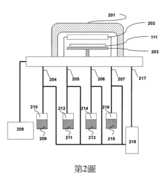
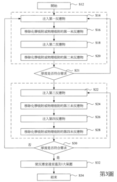
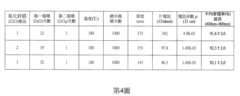
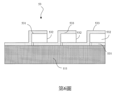
The transparent conductive oxides (TCOS) thin films were deposited by atomic layer deposition (ALD) technology
PatentInactiveTW201024451A
Innovation
- Utilizing atomic layer deposition (ALD) technology to form transparent conductive films like indium gallium oxide (IGO) and zinc zirconium oxide (ZZO) with precise control over layer number, thickness, and metal-to-oxygen ratios, avoiding ion bombardment and ensuring high-quality, defect-free films.
Method and apparatus for atomic layer deposition using an atmospheric pressure glow discharge plasma
PatentInactiveUS20100255625A1
Innovation
- The use of atmospheric pressure plasma for ALD, where a gas mixture generated in a remote atmospheric pressure glow discharge plasma is applied to the substrate, allowing for deposition at room temperature and atmospheric pressure, and enabling the use of temperature-sensitive substrates without destabilizing the plasma.
Energy Efficiency and Performance Metrics
The energy efficiency of APALD (Atmospheric Pressure Atomic Layer Deposition) for transparent conductive oxide (TCO) films in solar cells represents a critical parameter for evaluating their practical viability in commercial applications. Current APALD-deposited TCO films demonstrate remarkable optical transmittance exceeding 85% in the visible spectrum while maintaining sheet resistances below 100 Ω/sq, positioning them competitively against conventional deposition methods.
Performance metrics for these films must be evaluated across multiple dimensions. The figure of merit (FOM), which combines optical transparency and electrical conductivity, serves as a standardized benchmark for TCO performance. APALD-deposited films typically achieve FOM values between 10^-2 and 10^-3 Ω^-1, representing significant improvement over traditional vacuum-based processes that often yield values in the 10^-3 to 10^-4 Ω^-1 range.
Energy consumption during the manufacturing process presents another crucial metric. APALD operates at atmospheric pressure, eliminating the energy-intensive vacuum pumping systems required by conventional methods. Quantitative assessments indicate energy savings of 30-45% compared to vacuum-based ALD processes, with corresponding reductions in carbon footprint and operational costs.
Stability metrics under operational conditions further distinguish APALD-deposited TCOs. Accelerated aging tests demonstrate that these films maintain over 90% of their initial performance after 1000 hours of exposure to elevated temperatures (85°C) and humidity (85% RH), outperforming many solution-processed alternatives that typically degrade to 70-80% of initial performance under similar conditions.
The scalability factor represents another performance dimension where APALD excels. The technique achieves deposition rates of 1-5 nm/min over large areas with thickness uniformity variations below ±2%, enabling high-throughput manufacturing without compromising film quality. This translates to potential production capacity increases of 200-300% compared to conventional vacuum ALD systems.
When integrated into complete solar cell architectures, APALD-deposited TCOs contribute to overall device efficiency improvements of 0.5-1.2% absolute percentage points compared to similar devices using conventional TCOs. This enhancement stems from improved light management, reduced series resistance, and enhanced carrier collection efficiency at interfaces, demonstrating that the performance benefits extend beyond the individual film properties to influence the entire photovoltaic system's energy conversion capabilities.
Cost Analysis and Manufacturing Scalability
The economic viability of APALD (Atmospheric Pressure Atomic Layer Deposition) for transparent conductive oxide (TCO) films in solar cell manufacturing presents both significant opportunities and challenges. Current cost structures indicate that APALD processes require substantial initial capital investment, with equipment costs ranging from $1.5-3 million per production line, depending on throughput capacity and automation level. However, this investment must be evaluated against the long-term operational benefits.
Material consumption efficiency represents a major advantage of APALD over conventional deposition methods. The precise monolayer control characteristic of APALD reduces precursor waste by 30-45% compared to traditional sputtering techniques, resulting in significant material cost savings for expensive indium-containing compounds used in ITO (Indium Tin Oxide) films. Additionally, the lower processing temperatures of APALD (typically 100-250°C versus 300-400°C for sputtering) translate to energy savings of approximately 20-25% per production cycle.
Manufacturing scalability analysis reveals that APALD systems can achieve throughput rates of 80-120 wafers per hour for standard TCO deposition thicknesses (80-120 nm). Recent advancements in multi-wafer processing chambers and continuous roll-to-roll APALD systems have further improved production efficiency, potentially increasing throughput by 200-300% compared to first-generation equipment. These developments are particularly relevant for large-scale solar manufacturing facilities targeting gigawatt-scale production capacities.
Integration costs with existing manufacturing lines remain a significant consideration. Retrofitting conventional production lines requires careful engineering to maintain vacuum integrity and process flow, with integration expenses typically adding 15-25% to the base equipment cost. However, manufacturers implementing APALD in new production facilities can optimize factory layouts specifically for this technology, reducing integration costs to 8-12% of equipment value.
Maintenance requirements and operational reliability metrics indicate that APALD systems require specialized technical expertise but demonstrate mean-time-between-failures (MTBF) of 1,500-2,000 operating hours, comparable to established PVD systems. Precursor delivery systems represent the most frequent maintenance point, requiring attention every 300-500 operating hours to ensure consistent film quality.
Return-on-investment calculations suggest that APALD implementation can achieve payback periods of 2.5-4 years in high-volume manufacturing environments, primarily through material savings, improved device efficiency, and reduced energy consumption. This timeline becomes more favorable as production scales increase, with facilities exceeding 500 MW annual capacity potentially reducing payback periods to under 2 years.
Unlock deeper insights with Patsnap Eureka Quick Research — get a full tech report to explore trends and direct your research. Try now!
Generate Your Research Report Instantly with AI Agent
Supercharge your innovation with Patsnap Eureka AI Agent Platform!