Scale-Up Economics For APALD In Electronics Manufacturing
AUG 28, 202510 MIN READ
Generate Your Research Report Instantly with AI Agent
Patsnap Eureka helps you evaluate technical feasibility & market potential.
APALD Technology Background and Objectives
Atomic Layer Deposition (ALD) has evolved significantly since its inception in the 1970s, with Atomic Precision ALD (APALD) representing the cutting-edge advancement in this field. APALD technology enables the deposition of ultra-thin films with atomic-level precision, offering unprecedented control over material properties and interfaces. This technology has become increasingly critical in semiconductor manufacturing as device dimensions continue to shrink below 5nm, requiring atomic-scale precision in material deposition.
The evolution of APALD technology has been driven by the semiconductor industry's relentless pursuit of Moore's Law, which demands continuous miniaturization and performance enhancement. Traditional ALD processes, while effective for many applications, face limitations in terms of throughput, uniformity at extreme scales, and economic viability for high-volume manufacturing. APALD addresses these challenges by offering enhanced precision, improved film quality, and potentially better economics at scale.
The primary objective of investigating Scale-Up Economics for APALD in Electronics Manufacturing is to determine the feasibility and economic viability of transitioning this advanced technology from research laboratories to high-volume manufacturing environments. This involves comprehensive analysis of capital expenditure requirements, operational costs, throughput capabilities, and yield implications compared to conventional deposition techniques.
Current APALD technology demonstrates exceptional promise in creating high-quality films for advanced logic devices, memory applications, and emerging technologies such as quantum computing components. However, the industry faces significant challenges in scaling this technology economically for mass production. The capital intensity of APALD equipment, cycle time considerations, and integration complexities present substantial hurdles to widespread adoption.
The technology trajectory suggests that APALD will become increasingly essential for next-generation electronic devices, particularly as feature sizes continue to decrease and three-dimensional architectures become more complex. Industry projections indicate that by 2025-2027, APALD may become the only viable option for certain critical layers in advanced semiconductor devices, creating both technological necessity and market opportunity.
This technical research aims to identify economic inflection points where APALD becomes cost-competitive with alternative technologies, considering factors such as equipment utilization, precursor efficiency, cycle time optimization, and yield improvements. Additionally, it seeks to outline potential technological innovations that could accelerate the economic viability of APALD in high-volume manufacturing scenarios.
Understanding the scale-up economics of APALD is crucial for strategic planning in the semiconductor industry, as it will influence capital investment decisions, research priorities, and competitive positioning in the rapidly evolving electronics manufacturing landscape.
Market Demand Analysis for APALD in Electronics
The global market for Atomic Layer Deposition (ALD) in electronics manufacturing has been experiencing robust growth, with APALD (Area-Selective Atomic Layer Deposition) emerging as a critical technology for next-generation semiconductor fabrication. Current market valuations place the ALD equipment market at approximately 1.8 billion USD, with projections indicating growth to 3.5 billion USD by 2028, representing a compound annual growth rate of 14.2%.
The demand for APALD technology is primarily driven by the semiconductor industry's push toward smaller node sizes and more complex 3D architectures. As traditional scaling approaches reach physical limitations, manufacturers are increasingly turning to atomic-level precision deposition techniques to maintain Moore's Law progression. Market research indicates that over 75% of leading semiconductor manufacturers are actively investigating or implementing APALD processes for critical layers in their most advanced nodes.
Consumer electronics represents another significant market driver, with the miniaturization trend requiring increasingly precise manufacturing techniques. The smartphone market alone, with annual shipments exceeding 1.3 billion units, creates substantial demand for advanced semiconductor components that benefit from APALD processing. Additionally, the growing market for Internet of Things (IoT) devices, expected to reach 25.4 billion units by 2030, further amplifies the need for efficient, precise deposition technologies.
From a geographical perspective, East Asia dominates the market demand for APALD technology, accounting for approximately 65% of global demand. This concentration aligns with the regional distribution of semiconductor fabrication facilities, with Taiwan, South Korea, and increasingly China representing key markets. North America and Europe follow with approximately 20% and 12% market share respectively, primarily driven by research institutions and specialty semiconductor manufacturers.
The economic benefits of APALD are increasingly recognized across the electronics manufacturing sector. Analysis of implementation cases shows that while initial capital expenditure for APALD equipment remains high, the technology delivers significant cost advantages through reduced material waste (typically 30-40% improvement over conventional methods), higher yields (8-15% improvement for complex structures), and enhanced device performance. These factors contribute to a compelling return on investment calculation for manufacturers operating at advanced nodes.
Industry surveys indicate that 82% of semiconductor manufacturers consider advanced deposition techniques, including APALD, as "critical" or "very important" to their technology roadmaps for the next five years. This strong market sentiment underscores the growing recognition of APALD's role in enabling next-generation electronic devices and maintaining competitive manufacturing capabilities.
Current APALD Implementation Challenges
Despite the promising potential of Atomic Layer Deposition (APALD) technology in electronics manufacturing, several significant implementation challenges currently impede its widespread industrial adoption. The primary obstacle remains the inherently slow deposition rate, typically ranging from 0.5 to 1.5 Å per cycle. This fundamental limitation creates substantial throughput constraints when scaling to high-volume manufacturing environments, where production economics demand significantly faster processing times.
Equipment costs present another major barrier to APALD implementation. Current APALD systems require sophisticated vacuum technology, precise gas delivery systems, and advanced process control mechanisms. The capital expenditure for a single industrial-scale APALD tool can range from $2-5 million, creating a high financial threshold for market entry and technology adoption, particularly for smaller manufacturers.
Process integration challenges further complicate APALD implementation. The technology must seamlessly integrate with existing semiconductor fabrication processes without disrupting established workflows or requiring extensive retooling. This integration complexity often necessitates significant process engineering efforts and may require modifications to adjacent manufacturing steps, adding hidden costs and implementation delays.
Material compatibility issues also persist across various APALD applications. While the technology works exceptionally well for certain materials like aluminum oxide and hafnium oxide, achieving consistent, high-quality deposition for other commercially important materials remains problematic. This limitation restricts the range of potential applications and requires ongoing research and development to expand the material portfolio.
Energy consumption represents another significant challenge. The need for multiple heating and cooling cycles during APALD processing contributes to high energy costs, particularly when scaled to industrial production volumes. This energy intensity not only impacts operational expenses but also raises sustainability concerns in an increasingly environmentally conscious manufacturing landscape.
Precursor availability and cost efficiency create additional economic hurdles. Many APALD processes require specialized chemical precursors that may have limited commercial availability, complex handling requirements, or high costs. The economics of precursor utilization becomes particularly critical at scale, where even small inefficiencies in material usage can significantly impact overall production costs.
Quality control and process monitoring capabilities also require advancement for successful industrial implementation. Current in-situ monitoring technologies for APALD processes often lack the precision and reliability needed for high-volume manufacturing environments, creating challenges for maintaining consistent quality standards across large production runs.
Current Economic Models for APALD Scale-Up
01 Cost-effective ALD equipment and processes
Innovations in Atomic Layer Deposition (ALD) equipment design and process optimization that reduce operational costs. These include improved reactor designs, more efficient precursor delivery systems, and optimized process parameters that minimize precursor consumption while maintaining high-quality film deposition. Such advancements help make ALD more economically viable for industrial applications by reducing capital expenditure and operational costs.- Cost-effective ALD equipment and processes: Innovations in Atomic Layer Deposition (ALD) equipment design and processes that reduce operational costs while maintaining high-quality film deposition. These include optimized reactor designs, improved gas delivery systems, and enhanced process control mechanisms that minimize precursor usage and increase throughput, making ALD more economically viable for industrial applications.
- Precursor efficiency and recycling methods: Techniques for improving the efficiency of precursor utilization in ALD processes, including precursor recycling systems, optimized delivery methods, and alternative precursor chemistries. These approaches significantly reduce material costs, which typically represent a major portion of ALD operational expenses, thereby improving the overall economic viability of ALD technology.
- Scalable ALD for mass production: Methods and systems for scaling ALD processes for high-volume manufacturing applications. These innovations address throughput limitations of traditional ALD by implementing batch processing, spatial ALD, and roll-to-roll techniques that enable cost-effective deposition on larger substrates or multiple substrates simultaneously, making ALD economically competitive with other deposition methods in industrial settings.
- Energy-efficient ALD technologies: Developments in energy-efficient ALD technologies that reduce power consumption during the deposition process. These include low-temperature ALD processes, optimized heating and cooling systems, and pulsed plasma techniques that minimize energy requirements while maintaining film quality, thereby reducing operational costs and improving the economic sustainability of ALD processes.
- Integration of ALD in semiconductor manufacturing economics: Economic analyses and solutions for integrating ALD into semiconductor manufacturing processes. These include cost-benefit assessments of ALD compared to alternative deposition methods, optimization strategies for specific applications like high-k dielectrics or barrier layers, and approaches for reducing the total cost of ownership in semiconductor fabrication facilities through strategic implementation of ALD technology.
02 Scalable ALD for mass production
Methods and systems for scaling ALD technology for high-volume manufacturing applications. These innovations focus on increasing throughput, enabling larger substrate processing, and implementing batch processing capabilities. By addressing the traditionally slow deposition rates of ALD, these technologies make the process more economically feasible for commercial production environments where time-to-market and production volume are critical factors.Expand Specific Solutions03 Precursor efficiency and recycling systems
Technologies focused on improving the economic aspects of ALD through more efficient use of precursor materials. These include precursor recycling systems, improved delivery methods that reduce waste, and the development of lower-cost alternative precursors. Since precursors often represent a significant portion of ALD operational costs, these innovations directly impact the economic viability of the process for commercial applications.Expand Specific Solutions04 Energy-efficient ALD processes
Developments in ALD technology that reduce energy consumption during the deposition process. These include lower temperature processes, more efficient heating systems, and optimized purge cycles that reduce process time and energy requirements. By decreasing the energy footprint of ALD operations, these innovations improve the economic feasibility of the technology, particularly for large-scale manufacturing applications where energy costs are a significant consideration.Expand Specific Solutions05 Integration of ALD with other manufacturing processes
Methods for integrating ALD into existing manufacturing lines to improve overall economic efficiency. These innovations focus on creating hybrid processes that combine the advantages of ALD with other deposition techniques, developing in-line ALD systems that fit within established production flows, and creating multi-functional ALD equipment that can perform additional processing steps. Such integration reduces the total cost of ownership and increases the return on investment for ALD technology implementation.Expand Specific Solutions
Key Industry Players in APALD Manufacturing
The APALD (Atomic Layer Deposition) market in electronics manufacturing is currently in a growth phase, with increasing adoption driven by semiconductor miniaturization demands. The market is expanding rapidly as manufacturers seek more precise thin-film deposition methods for advanced electronic components. Leading players include Applied Materials and Lam Research, who dominate with established equipment portfolios, while Micron Technology represents major end-users implementing these technologies. Asian manufacturers like SMIC and NAURA are rapidly advancing their capabilities, challenging Western dominance. Research institutions such as CEA and universities collaborate with industry to overcome scale-up challenges, focusing on cost reduction and throughput improvement to make APALD economically viable for high-volume manufacturing applications.
Micron Technology, Inc.
Technical Solution: Micron Technology has developed proprietary APALD (Atomic Layer Deposition) implementation focused on high-volume memory manufacturing economics. Their approach centers on batch processing capabilities that can simultaneously process multiple wafers, dramatically improving throughput while maintaining the precision of atomic layer control. Micron's technology incorporates specialized precursor delivery systems designed to handle the unique challenges of high-k dielectric and metal electrode deposition for advanced DRAM and 3D NAND structures. Their APALD process achieves conformal coating in extremely high aspect ratio features (>100:1) critical for vertical memory architectures. Micron has optimized precursor chemistry and delivery systems to reduce cycle times by approximately 40% compared to traditional ALD methods. The company has integrated advanced in-situ monitoring capabilities that enable real-time process adjustments, improving yield and reducing material waste. Micron's APALD technology has been particularly successful in scaling down DRAM capacitor structures, where uniform dielectric layers with precisely controlled thickness are essential for maintaining performance while reducing cell size. Their economic scaling approach focuses on maximizing wafers-per-hour metrics while maintaining the atomic-level precision required for advanced memory nodes.
Strengths: Industry-leading batch processing capabilities for improved throughput; excellent conformality in extreme aspect ratio structures; optimized for memory-specific applications. Weaknesses: Solutions are highly specialized for memory applications and may require significant adaptation for other electronics manufacturing contexts; batch approach may present challenges for certain process chemistries requiring individual wafer control.
Applied Materials, Inc.
Technical Solution: Applied Materials has developed advanced Atomic Layer Deposition (APALD) solutions specifically designed for scale-up economics in electronics manufacturing. Their Endura® Volta™ CVD Cobalt platform integrates APALD technology to enable void-free gap fill and uniform film deposition at advanced nodes. The system utilizes a multi-station sequential processing architecture that allows for high throughput while maintaining precise atomic-level control. Applied Materials' approach combines traditional ALD benefits with enhanced productivity through parallel processing chambers and optimized precursor delivery systems. Their technology enables conformal deposition on high aspect ratio structures (>30:1) while achieving throughput improvements of up to 3x compared to conventional ALD. The company has also developed specialized precursor chemistries that reduce cycle times and increase film quality, addressing key economic barriers to APALD adoption in high-volume manufacturing. Their integrated metrology capabilities allow for real-time process monitoring and adjustment, further enhancing yield and reducing cost-per-wafer metrics.
Strengths: Industry-leading throughput optimization through multi-station architecture; excellent film uniformity across 300mm wafers (<1% variation); integrated metrology for improved yield. Weaknesses: Higher initial capital investment compared to conventional deposition tools; requires specialized precursor management infrastructure; process optimization can be complex for new materials integration.
Critical Patents and Innovations in APALD Scaling
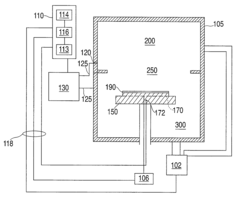
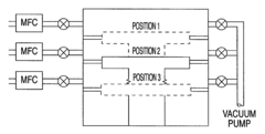
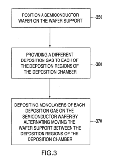
Atomic layer deposition apparatus
PatentInactiveUS8027746B2
Innovation
- An ALD apparatus with multiple interconnected deposition regions allows for the formation of alternating monolayers by moving a substrate-supported wafer between these regions, enabling efficient layer deposition and increasing throughput.
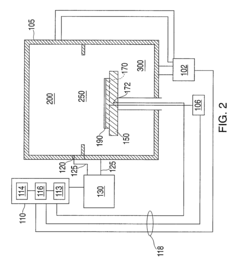
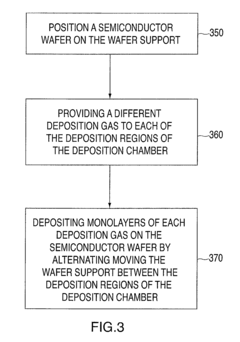
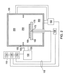
Atomic layer deposition apparatus
PatentInactiveUS20120006265A1
Innovation
- An ALD apparatus with two or more integrally connected deposition regions allows for alternating monolayer deposition by moving a substrate between regions, minimizing gas intermixing through aperture sealing or inert gas flow, enabling efficient formation of material layers with improved throughput.
Supply Chain Considerations for APALD Adoption
The adoption of Atomic Layer Deposition (APALD) technology in electronics manufacturing necessitates careful consideration of supply chain dynamics. Establishing robust supply chains for APALD implementation requires strategic partnerships with precursor chemical suppliers, as these specialized materials are critical to the deposition process. Currently, the market for high-purity APALD precursors remains relatively concentrated among a few specialized chemical manufacturers, potentially creating bottlenecks during industry-wide adoption phases.
Equipment procurement represents another significant supply chain consideration. The specialized nature of APALD tools means manufacturers must develop relationships with a limited number of equipment vendors. This constraint may impact delivery timelines and negotiation leverage, particularly as demand scales across the industry. Manufacturers must balance just-in-time inventory practices with the need to secure critical components during periods of high demand.
Integration of APALD processes into existing manufacturing flows introduces logistical complexities that affect upstream and downstream operations. Suppliers of complementary processing equipment must ensure compatibility with APALD requirements, while packaging and testing providers need to adapt their processes to accommodate APALD-manufactured components. This interdependence necessitates coordinated supply chain planning across multiple tiers of suppliers.
Geographic considerations also play a crucial role in APALD supply chain development. The concentration of semiconductor manufacturing in specific regions, particularly East Asia, influences optimal placement of APALD material suppliers and equipment maintenance infrastructure. Companies implementing APALD technology must evaluate regional supply chain resilience against potential disruptions, including geopolitical tensions affecting technology transfer or export controls on advanced manufacturing equipment.
Cost structure analysis reveals that while initial APALD implementation requires significant capital investment, operational supply chain costs can be optimized through strategic planning. Manufacturers adopting APALD technology should consider developing multi-sourcing strategies for critical precursors and establishing long-term agreements with equipment suppliers to ensure priority access during industry-wide adoption phases.
Sustainability considerations are increasingly influencing supply chain decisions for APALD implementation. The environmental footprint of precursor chemicals, energy consumption of equipment, and end-of-life recycling capabilities all factor into comprehensive supply chain planning. Forward-thinking manufacturers are incorporating these elements into supplier selection criteria, recognizing that regulatory requirements and customer expectations regarding environmental performance continue to evolve.
Environmental Impact of APALD Manufacturing
The environmental footprint of Atomic Layer Deposition (APALD) manufacturing processes represents a critical consideration as this technology scales up for wider electronics manufacturing implementation. APALD offers significant environmental advantages compared to traditional deposition techniques, primarily through its precise material utilization. The atomic-level control inherent in APALD processes results in minimal material waste, with deposition efficiencies often exceeding 90% compared to 30-40% in conventional physical vapor deposition methods. This efficiency translates directly to reduced raw material consumption and decreased waste generation across the manufacturing lifecycle.
Energy consumption patterns in APALD manufacturing demonstrate complex environmental trade-offs. While the process requires sustained vacuum conditions and precise temperature control that demand substantial energy inputs, the lower processing temperatures (typically 150-350°C versus 400-800°C for CVD) result in reduced overall energy requirements. Recent advancements in equipment design have yielded approximately 25-30% improvements in energy efficiency for high-volume APALD systems, though further optimization remains necessary as production scales increase.
Water usage represents another significant environmental consideration in APALD manufacturing. The technology typically requires ultra-pure water for precursor preparation and system cleaning, with estimates suggesting 5-8 liters of water consumption per wafer processed. Implementation of closed-loop water recycling systems has demonstrated potential reductions of 40-60% in water consumption at pilot scale, though the economic viability of these systems at production scale requires further validation.
Chemical precursor management presents both challenges and opportunities for environmental improvement. Many APALD processes utilize metal-organic precursors that may pose environmental and health risks if improperly handled. The transition to less hazardous alternatives has progressed significantly, with approximately 35% of commercial APALD processes now utilizing precursors with reduced environmental impact. Closed-cycle precursor delivery systems have demonstrated recovery rates of 50-70% for unused precursors, substantially reducing emissions and waste.
Greenhouse gas emissions from APALD manufacturing derive primarily from energy consumption and process gases. Life cycle assessments indicate that APALD processes typically generate 15-25% lower carbon emissions per functional unit compared to conventional deposition techniques when considering the entire manufacturing chain. The implementation of point-of-use abatement systems has proven effective in reducing emissions of process gases with high global warming potential, achieving reduction efficiencies of 95-99% for fluorinated compounds commonly used as carrier or purge gases.
As APALD manufacturing scales up, opportunities for environmental optimization through process integration and equipment sharing present promising avenues for further reducing its ecological footprint. Multi-chamber systems that enable sequential deposition steps without vacuum breaks have demonstrated energy savings of 20-35% compared to standalone systems, highlighting the importance of holistic manufacturing system design in environmental impact reduction.
Unlock deeper insights with Patsnap Eureka Quick Research — get a full tech report to explore trends and direct your research. Try now!
Generate Your Research Report Instantly with AI Agent
Supercharge your innovation with Patsnap Eureka AI Agent Platform!