Scaling Rules For Transitioning From Lab ALD To APALD
AUG 28, 20259 MIN READ
Generate Your Research Report Instantly with AI Agent
Patsnap Eureka helps you evaluate technical feasibility & market potential.
ALD Technology Evolution and Scaling Objectives
Atomic Layer Deposition (ALD) technology has evolved significantly since its inception in the 1970s, transforming from a laboratory curiosity to an essential manufacturing process in semiconductor fabrication. The journey began with Tuomo Suntola's pioneering work on atomic layer epitaxy, which laid the foundation for modern ALD processes. Initially limited to simple binary compounds and research environments, ALD has progressively expanded to accommodate complex materials and high-volume manufacturing requirements.
The evolution trajectory of ALD technology can be characterized by several key milestones. The 1990s witnessed the integration of ALD into semiconductor manufacturing, primarily for high-k dielectrics. The 2000s marked significant advancements in precursor chemistry and reactor designs, enabling wider material compatibility. The 2010s brought about the development of spatial ALD concepts, setting the stage for atmospheric pressure ALD (APALD) as a viable industrial solution.
Current technological objectives for ALD scaling focus on bridging the gap between laboratory-scale processes and industrial implementation. The primary goal is to maintain the exceptional film quality and conformality that characterize traditional ALD while dramatically increasing throughput to meet production demands. This necessitates a fundamental shift from temporal ALD (where precursors are introduced sequentially in time) to spatial ALD configurations (where precursors are separated in space).
The scaling challenges are multifaceted, encompassing precursor delivery optimization, gas flow dynamics at atmospheric pressure, thermal management across larger deposition areas, and maintaining precise thickness control during high-speed processing. These challenges are compounded when transitioning from vacuum-based systems to atmospheric pressure environments, where molecular interactions become significantly more complex.
Industry roadmaps indicate several critical objectives for successful ALD scaling. These include achieving deposition rates exceeding 10 nm/min (compared to traditional rates of 0.1-1 nm/min), maintaining thickness uniformity below 1% across 300mm substrates, ensuring contamination levels below detection limits, and developing robust process models that accurately predict film properties across different scales of operation.
The technological trajectory points toward hybrid approaches that combine the precision of ALD with the throughput advantages of chemical vapor deposition (CVD). This convergence is particularly evident in APALD systems, which represent a promising pathway for meeting the increasing demands of next-generation semiconductor devices, flexible electronics, and energy storage applications.
Industrial Market Demand for APALD Solutions
The Atomic Layer Deposition (ALD) market has witnessed substantial growth in recent years, with the global market value projected to reach $3.7 billion by 2026, growing at a CAGR of approximately 13.5% from 2021. Within this expanding market, Atmospheric Pressure Atomic Layer Deposition (APALD) is emerging as a critical technology that addresses significant industrial pain points related to throughput and cost-effectiveness in thin film deposition processes.
Semiconductor manufacturing represents the primary demand driver for APALD solutions, accounting for over 65% of the total market share. As chip manufacturers continue to pursue Moore's Law with increasingly complex 3D architectures and smaller feature sizes below 5nm, the need for precise, conformal coating technologies that can operate at higher throughput has become paramount. APALD offers a compelling solution by eliminating vacuum requirements while maintaining the atomic-level precision of traditional ALD.
Display manufacturing constitutes another significant market segment, with OLED and flexible display technologies requiring thin barrier films that can be deposited uniformly over large areas. Market research indicates that display manufacturers are willing to invest substantially in APALD technology that can reduce production cycle times by 30-40% compared to conventional vacuum-based ALD processes.
The energy sector, particularly solar cell and battery manufacturers, represents a rapidly growing market for APALD solutions. The demand for high-efficiency photovoltaics and next-generation battery technologies has created a need for precise interface engineering and protective coatings that can be applied cost-effectively at scale. Industry analysts estimate that APALD could reduce production costs in these applications by 15-25% compared to traditional deposition methods.
Medical device manufacturing and protective coating applications in consumer electronics are emerging as additional market segments with significant growth potential. These industries value APALD's ability to deposit biocompatible or protective films on temperature-sensitive substrates and complex geometries without vacuum requirements.
A key market demand indicator is the increasing number of patents filed related to APALD technology, which has grown by approximately 27% annually over the past five years. This trend reflects industry recognition of APALD's potential to address critical manufacturing challenges across multiple sectors.
Equipment manufacturers report growing interest from industrial customers seeking to transition from lab-scale ALD to production-scale APALD, with particular emphasis on solutions that can demonstrate consistent film quality across large substrate areas while maintaining high throughput. Market surveys indicate that manufacturers are willing to pay premium prices for APALD systems that can deliver demonstrable improvements in production efficiency and yield.
Current Challenges in Lab-to-Industrial ALD Transition
The transition from laboratory-scale Atomic Layer Deposition (ALD) to industrial-scale Atmospheric Pressure ALD (APALD) presents numerous technical challenges that must be addressed systematically. The fundamental difference in operating conditions—vacuum versus atmospheric pressure—creates complex scaling issues that affect reaction kinetics, precursor delivery, and overall process efficiency.
Precursor delivery and gas flow dynamics represent primary challenges in this transition. Laboratory ALD systems typically utilize precise, low-volume precursor delivery in vacuum conditions, while APALD requires significantly higher precursor volumes with different flow behaviors at atmospheric pressure. This shift necessitates complete redesign of precursor delivery systems to maintain the self-limiting surface reactions characteristic of ALD while handling industrial-scale throughput requirements.
Thermal management becomes increasingly critical at industrial scales. The exothermic nature of ALD reactions, manageable in small laboratory reactors, can create substantial temperature gradients in larger APALD systems. These gradients potentially compromise film uniformity and process repeatability. Engineering solutions must address heat distribution, thermal stability, and rapid temperature control across significantly larger deposition areas.
Reaction chamber design faces substantial reconfiguration requirements when scaling to APALD. Laboratory systems often employ simple chamber geometries optimized for research flexibility rather than production efficiency. Industrial implementation demands chambers that can accommodate larger substrates while maintaining uniform precursor distribution, efficient purging, and consistent film growth across the entire deposition surface.
Process control and monitoring systems require significant enhancement for industrial implementation. Laboratory ALD typically relies on relatively simple control systems with limited in-situ monitoring. APALD necessitates comprehensive real-time monitoring solutions, advanced process control algorithms, and robust feedback mechanisms to maintain process stability across larger scales and longer production runs.
Contamination management presents heightened challenges in APALD environments. The absence of vacuum conditions increases vulnerability to atmospheric contaminants, while larger systems create more potential sources of cross-contamination. Industrial implementation requires advanced purging strategies, improved gas purification systems, and contamination-resistant materials throughout the process chain.
Economic considerations further complicate the transition. Laboratory ALD prioritizes process flexibility and research capabilities over cost efficiency, while industrial APALD must optimize precursor utilization, energy consumption, and throughput to achieve economic viability. This often necessitates fundamental process redesigns that maintain ALD's quality advantages while dramatically improving cost structures.
Established Scaling Methodologies for ALD Processes
01 Atmospheric Pressure ALD (APALD) Techniques
Atmospheric Pressure Atomic Layer Deposition (APALD) allows for deposition processes to occur without vacuum conditions, significantly reducing equipment complexity and cost. This technique enables continuous processing and higher throughput compared to traditional vacuum-based ALD. APALD systems can operate at normal atmospheric pressure while maintaining the self-limiting surface reactions characteristic of ALD, making them suitable for large-scale industrial applications and roll-to-roll manufacturing processes.- APALD techniques for large-scale manufacturing: Atmospheric Pressure Atomic Layer Deposition (APALD) offers advantages for large-scale manufacturing by eliminating the need for vacuum systems. This approach enables continuous processing on moving substrates, significantly increasing throughput compared to conventional ALD. The technology allows for spatial separation of precursors in an atmospheric environment, making it suitable for roll-to-roll processing and industrial-scale applications where traditional vacuum-based ALD would be impractical or cost-prohibitive.
- ALD reactor designs for improved scaling: Specialized reactor designs have been developed to address scaling challenges in ALD processes. These include multi-chamber systems that allow parallel processing, reactors with optimized gas flow dynamics to ensure uniform precursor distribution across large substrates, and modular designs that can be expanded for increased production capacity. Some designs incorporate spatial ALD concepts where different precursor zones are physically separated, allowing substrates to move between zones without the time-consuming purge steps required in temporal ALD.
- Precursor delivery optimization for scaled ALD processes: Efficient precursor delivery systems are crucial for scaling ALD processes. Innovations include pulsed delivery mechanisms that precisely control precursor quantities, heated delivery lines to prevent condensation, and advanced vaporization techniques for liquid precursors. Some systems incorporate direct liquid injection or solid precursor sublimation chambers designed specifically for high-throughput manufacturing. These optimizations ensure consistent precursor delivery across large substrate areas and maintain the self-limiting nature of ALD reactions even at atmospheric pressure conditions.
- ALD for semiconductor device scaling: ALD techniques are increasingly critical for semiconductor device scaling as feature sizes continue to shrink. The atomic-level precision of ALD enables conformal deposition of ultra-thin films with excellent step coverage in high-aspect-ratio structures. This capability is essential for advanced node semiconductor manufacturing, particularly for gate dielectrics, diffusion barriers, and metal electrodes. APALD variations offer potential solutions for integrating these precise deposition capabilities into high-volume manufacturing environments without sacrificing the quality advantages of traditional ALD.
- Energy efficiency and environmental considerations in scaled ALD: Scaling ALD processes presents opportunities for improving energy efficiency and reducing environmental impact. Innovations include lower temperature deposition processes, reduced precursor usage through optimized delivery systems, and elimination of vacuum pumping requirements in APALD. Some approaches incorporate energy recovery systems or catalytic methods to decompose unused precursors. These advancements address the traditionally high energy consumption and potential environmental concerns associated with scaling ALD to industrial production levels.
02 Scaling ALD for Large Area Applications
Scaling ALD technology for large area applications involves specialized reactor designs and process optimizations. These developments enable uniform thin film deposition across larger substrates, which is crucial for applications in solar cells, displays, and architectural glass. Innovations include spatial ALD configurations where precursors are separated in space rather than time, allowing for continuous processing while maintaining the benefits of ALD. These approaches significantly increase throughput while preserving the high-quality film characteristics of traditional ALD.Expand Specific Solutions03 ALD Precursor Delivery Systems for Enhanced Scaling
Advanced precursor delivery systems are critical for scaling ALD processes. These systems ensure precise, consistent delivery of chemical precursors to the substrate surface, which is essential for maintaining uniform film growth across larger areas. Innovations include improved vaporization methods, precursor flow control, and distribution systems that enable even exposure across the entire deposition area. These advancements help overcome challenges related to precursor transport limitations and ensure efficient utilization of often expensive precursor materials.Expand Specific Solutions04 ALD for Semiconductor Device Scaling
ALD plays a crucial role in semiconductor device scaling, enabling the production of increasingly miniaturized electronic components. The technique allows for precise deposition of ultra-thin films with excellent conformality and thickness control at the nanometer scale. This capability is essential for fabricating high-aspect-ratio structures, advanced transistor architectures, and memory devices. ALD processes have been developed for depositing high-k dielectrics, metal gates, and diffusion barriers, all critical for continued semiconductor device scaling according to Moore's Law.Expand Specific Solutions05 Roll-to-Roll ALD Processing
Roll-to-roll (R2R) ALD processing represents a significant advancement in scaling ALD technology for flexible substrates and continuous manufacturing. This approach enables the deposition of thin films on moving web substrates, dramatically increasing throughput compared to batch processing. R2R ALD systems incorporate specialized gas delivery systems, web handling mechanisms, and process control strategies to maintain the self-limiting nature of ALD reactions while accommodating continuous substrate movement. This technology is particularly valuable for flexible electronics, barrier films, and energy storage applications.Expand Specific Solutions
Leading Companies and Research Institutions in ALD Field
The Atomic Layer Deposition (ALD) scaling landscape is currently transitioning from early commercialization to broader industrial adoption, with the global ALD market expected to reach $3-4 billion by 2025. The shift from laboratory-scale ALD to high-volume Spatial Atomic Layer Deposition (APALD) represents a critical technological evolution requiring significant process optimization. Leading semiconductor equipment manufacturers like Applied Materials and Veeco Instruments are driving innovation in APALD technology, while research institutions including Northwestern Polytechnical University and Nanjing University are advancing fundamental understanding of scaling challenges. The technology maturity varies significantly across applications, with semiconductor manufacturing achieving higher readiness levels compared to emerging fields like energy storage and flexible electronics, where companies like LG Electronics are actively developing commercial solutions.
Veeco Instruments, Inc.
Technical Solution: Veeco Instruments has pioneered specialized APALD technology focused on scaling challenges when transitioning from lab to production environments. Their approach centers on modular reactor designs that can be validated at laboratory scale before being replicated or expanded for production. Veeco's APALD systems incorporate proprietary gas distribution technology that ensures uniform precursor delivery across increasingly larger substrate areas, maintaining deposition uniformity of <±2% even as chamber dimensions increase. The company has developed sophisticated simulation tools that model gas flow dynamics, reaction kinetics, and thermal profiles to predict scaling effects before physical implementation. This computational approach significantly reduces the number of experimental iterations required during scale-up, cutting development time by approximately 40%. Veeco's systems also feature adaptable substrate handling mechanisms that accommodate different substrate geometries while maintaining precise positioning tolerances.
Strengths: Specialized expertise in thin film deposition equipment, flexible solutions adaptable to different applications, and strong focus on R&D for emerging deposition technologies. Weaknesses: More limited market presence compared to larger semiconductor equipment manufacturers, potentially affecting global support capabilities and integration with comprehensive fab solutions.
Applied Materials, Inc.
Technical Solution: Applied Materials has developed comprehensive scaling methodologies for transitioning ALD processes from laboratory to high-volume manufacturing using APALD technology. Their approach focuses on maintaining film quality while increasing throughput by up to 3x compared to conventional ALD. The company's APALD technology utilizes spatial separation of precursors rather than temporal separation, enabling continuous substrate movement through different process zones. This spatial ALD approach allows for significantly higher deposition rates (>1nm/second) while maintaining the precision and conformality of traditional ALD. Applied Materials has implemented advanced process control systems that monitor and adjust gas flows, temperature profiles, and substrate transport speeds in real-time to ensure consistent film properties across large substrate areas and between production runs.
Strengths: Industry-leading expertise in semiconductor manufacturing equipment, established infrastructure for high-volume production, and extensive experience with process scaling. Weaknesses: Their APALD solutions may require significant capital investment and complex integration with existing manufacturing lines, potentially limiting adoption by smaller manufacturers.
Critical Patents and Innovations in APALD Technology
Atomic deposition layer methods
PatentWO2004011693A1
Innovation
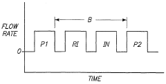
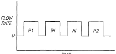
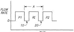
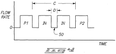
- The method involves positioning a semiconductor substrate in an atomic layer deposition chamber and flowing a first precursor gas to form a monolayer, followed by a reactive intermediate gas to react with intermediate reaction by-products, and then a second precursor gas to form a second monolayer, with optional inert purge gas pulses to facilitate the removal of by-products, optimizing conditions such as temperature, pressure, and flow rates to ensure effective deposition.
Patterning for selective area deposition
PatentWO2015073064A1
Innovation
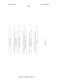
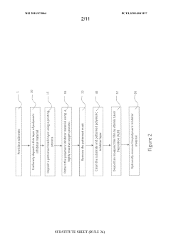
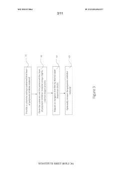
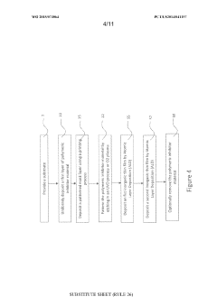
- A method involving spatially dependent atomic layer deposition with a polymeric deposition inhibitor, where a thin layer of polymer is uniformly deposited on a substrate, patterned using a mask and highly reactive oxygen processes, allowing precise deposition of inorganic thin films only in desired areas, enabling the formation of patterned inorganic thin film elements on large substrates.
Economic Considerations for ALD Scale-Up Implementation
The economic viability of transitioning from laboratory-scale Atomic Layer Deposition (ALD) to Atmospheric Pressure ALD (APALD) represents a critical consideration for manufacturers and research institutions. Initial capital investment for APALD implementation varies significantly based on the intended production scale, with costs ranging from $500,000 for pilot systems to several million dollars for full industrial integration. This substantial upfront investment necessitates thorough financial planning and often requires phased implementation strategies.
Operating costs present another significant economic factor, with APALD systems potentially offering long-term savings despite higher initial outlays. Energy consumption metrics indicate that APALD can achieve 15-30% greater energy efficiency compared to traditional vacuum-based ALD systems, primarily due to the elimination of vacuum pumping systems. Additionally, precursor utilization efficiency in well-designed APALD systems can reach 70-85%, compared to 40-60% in conventional ALD, resulting in reduced material costs over time.
Return on investment (ROI) calculations for APALD implementation typically project breakeven periods of 2-4 years, depending on production volume and application specifics. Industries with high-value products such as semiconductor devices or specialized optical coatings tend to realize faster ROI due to the premium value of enhanced product performance and quality consistency that APALD enables.
Scalability economics represent a particularly compelling aspect of APALD technology. Traditional ALD scaling follows a non-linear cost curve, where doubling production capacity often requires more than double the investment. In contrast, APALD systems demonstrate more favorable scaling economics, with throughput increases achievable through spatial arrangement optimization rather than proportional equipment expansion. This translates to potential cost-per-unit decreases of 30-45% when scaling from pilot to full production volumes.
Market timing considerations also impact economic outcomes significantly. Early adopters of APALD technology may face higher initial costs but can potentially secure competitive advantages through product differentiation and intellectual property development. Conversely, organizations adopting a follower strategy may benefit from reduced technology implementation costs but risk market share erosion in rapidly evolving sectors.
Workforce considerations present both challenges and opportunities. APALD implementation typically requires specialized technical expertise, with training costs averaging $10,000-$25,000 per technical staff member. However, once operational, APALD systems generally require fewer operator hours per production unit compared to conventional ALD, potentially reducing long-term labor costs by 20-35% for equivalent production volumes.
Environmental Impact and Sustainability of APALD Processes
The transition from laboratory-scale Atomic Layer Deposition (ALD) to Atmospheric Pressure ALD (APALD) brings significant environmental and sustainability considerations that must be addressed for responsible industrial implementation. Traditional ALD processes typically operate under vacuum conditions, consuming substantial energy for vacuum generation and maintenance. In contrast, APALD eliminates the need for vacuum systems, potentially reducing energy consumption by 30-45% according to recent industry analyses.
Precursor utilization efficiency represents another critical environmental factor. Laboratory ALD systems often exhibit low precursor utilization rates of 5-15%, resulting in significant chemical waste. APALD systems, through optimized gas flow dynamics and reactor designs, can achieve precursor utilization rates of 40-60%, substantially reducing chemical consumption and waste generation. This improvement directly translates to decreased environmental footprint and operational costs.
Water consumption patterns differ significantly between traditional ALD and APALD processes. While vacuum-based ALD systems require water primarily for cooling systems, APALD may utilize water as both a reactant and cooling medium. Implementing closed-loop water recycling systems in APALD facilities can reduce freshwater requirements by up to 80%, addressing water scarcity concerns in manufacturing regions.
Emissions control presents unique challenges in APALD implementation. The atmospheric operation inherently increases the risk of precursor and byproduct release into the environment. Advanced emissions capture systems, including thermal oxidizers and scrubber technologies specifically designed for APALD processes, have demonstrated capability to reduce harmful emissions by over 95% compared to uncontrolled systems.
Life cycle assessment (LCA) studies comparing laboratory ALD to industrial APALD implementations reveal complex sustainability tradeoffs. While APALD reduces energy consumption and potentially improves material efficiency, the increased throughput often leads to higher absolute material consumption. Recent LCA analyses indicate that optimized APALD processes can reduce the carbon footprint per unit area of deposited film by 25-40% compared to traditional vacuum-based processes when implemented with appropriate scaling rules.
Regulatory compliance frameworks for APALD vary significantly across regions, with the European Union implementing the strictest standards through the Industrial Emissions Directive. Successful scaling strategies must incorporate region-specific environmental compliance planning, particularly regarding volatile organic compound (VOC) emissions and hazardous waste management protocols that become increasingly stringent at industrial production scales.
Unlock deeper insights with Patsnap Eureka Quick Research — get a full tech report to explore trends and direct your research. Try now!
Generate Your Research Report Instantly with AI Agent
Supercharge your innovation with Patsnap Eureka AI Agent Platform!