SALD For Transparent Barrier Films In OLED Displays
AUG 28, 20259 MIN READ
Generate Your Research Report Instantly with AI Agent
Patsnap Eureka helps you evaluate technical feasibility & market potential.
SALD Technology Evolution and Objectives
Spatial Atomic Layer Deposition (SALD) technology represents a significant evolution in thin film deposition methods, emerging as a response to the limitations of conventional Atomic Layer Deposition (ALD). The journey of SALD began in the early 2000s when researchers sought to overcome the throughput constraints of traditional ALD while maintaining its exceptional film quality and conformality advantages. Unlike conventional ALD, which operates in a temporal sequence, SALD separates precursors spatially, allowing for continuous deposition and dramatically increased throughput—a critical factor for industrial-scale production.
The evolution of SALD has been marked by several key technological milestones. Initially developed for photovoltaic applications, the technology has progressively expanded into display technologies, particularly OLED displays, where ultra-thin, defect-free barrier films are essential. Early SALD systems faced challenges with precursor separation and uniformity across large areas, but innovations in gas flow dynamics and precursor delivery systems have substantially improved these aspects over the past decade.
From 2010 to 2015, significant advancements were made in atmospheric pressure SALD, eliminating the need for vacuum systems and further enhancing production efficiency. The period from 2015 to 2020 saw the development of roll-to-roll SALD systems, enabling continuous processing of flexible substrates—a crucial capability for next-generation flexible OLED displays.
The primary objective of current SALD research for OLED barrier films is to achieve transparent films with water vapor transmission rates (WVTR) below 10^-6 g/m²/day while maintaining optical transparency above 90% in the visible spectrum. These parameters are essential for ensuring the longevity and performance of OLED devices, which are extremely sensitive to moisture and oxygen penetration.
Additional technical objectives include developing multi-layer barrier architectures that combine inorganic layers (typically metal oxides like Al₂O₃ or ZnO) with organic interlayers to create tortuous paths for water vapor diffusion. Researchers are also focusing on reducing deposition temperatures to enable compatibility with temperature-sensitive substrates such as flexible polymers, targeting processes below 100°C without compromising film quality.
Looking forward, the technology roadmap for SALD in OLED applications aims to scale up to Gen 8+ substrate sizes while maintaining nanometer-level thickness uniformity across the entire deposition area. Process integration with existing display manufacturing lines represents another critical objective, requiring seamless compatibility with upstream and downstream processes in OLED production.
Market Analysis for OLED Barrier Films
The OLED display market has experienced substantial growth over the past decade, with a market value reaching $48.5 billion in 2022 and projected to surpass $73.2 billion by 2026, representing a CAGR of 10.8%. Within this ecosystem, barrier films constitute a critical component, with their market value estimated at $1.2 billion in 2022 and expected to grow to $2.1 billion by 2026.
The demand for high-performance transparent barrier films is primarily driven by the rapid expansion of OLED technology across multiple sectors. The consumer electronics segment, particularly smartphones and premium televisions, currently accounts for approximately 65% of the total barrier film consumption. The automotive industry represents an emerging high-growth sector, with OLED dashboard displays and interior lighting systems expected to grow at 24% annually through 2025.
Geographically, East Asia dominates the production landscape, with South Korea, Japan, and China collectively manufacturing over 70% of global OLED barrier films. However, European and North American markets are showing increased interest in domestic production capabilities to reduce supply chain vulnerabilities, as evidenced by recent investments in advanced manufacturing facilities.
The barrier film market is segmented by technology type, with traditional vacuum-deposited multilayer films currently holding 58% market share. SALD-based solutions, though representing only 12% of the current market, are projected to grow at 32% annually due to their superior performance characteristics and potential for cost reduction at scale.
End-user requirements are increasingly stringent, with display manufacturers demanding water vapor transmission rates (WVTR) below 10^-6 g/m²/day and oxygen transmission rates (OTR) below 10^-3 cm³/m²/day. Additionally, optical transparency exceeding 90% in the visible spectrum and flexibility supporting bend radii below 1mm have become standard requirements for next-generation flexible displays.
Price sensitivity varies significantly by application segment. While premium smartphone manufacturers can absorb barrier film costs of $15-20 per square meter, emerging applications in wearables and IoT devices require solutions below $8 per square meter to enable mass adoption. This price-performance gap represents a significant market opportunity for SALD technology, which promises to deliver high-performance barriers at reduced costs through more efficient material utilization and higher throughput manufacturing processes.
SALD Technical Challenges in Display Industry
The implementation of SALD technology for transparent barrier films in OLED displays faces several significant technical challenges that require innovative solutions. The primary obstacle lies in achieving uniform deposition across large-area substrates while maintaining high throughput. Current SALD systems struggle to deliver consistent film thickness and quality when scaled to Gen 8 or larger display manufacturing dimensions, resulting in barrier performance variations that compromise OLED longevity.
Material compatibility presents another critical challenge, as SALD processes must operate at temperatures below 100°C to prevent damage to temperature-sensitive OLED components and flexible substrates. This temperature constraint limits precursor options and reaction kinetics, potentially affecting film quality and deposition rates. Additionally, the chemical compatibility between successive material layers in multi-layer barrier stacks demands careful precursor selection and process optimization.
Precursor delivery systems for SALD require substantial refinement to ensure precise, controlled gas flow dynamics across large substrate areas. Current gas distribution mechanisms often create non-uniform concentration gradients, leading to thickness variations and potential defect formation in the barrier films. These defects can become pathways for moisture and oxygen permeation, compromising the barrier's effectiveness.
The industry also faces challenges in developing in-line quality control and metrology tools capable of detecting nanoscale defects in transparent barrier films at production speeds. Without reliable real-time monitoring, manufacturers cannot guarantee consistent water vapor transmission rates (WVTR) below the critical threshold of 10^-6 g/m²/day required for OLED protection.
Integration of SALD into existing production lines presents significant engineering challenges. The technology must be compatible with roll-to-roll or sheet-to-sheet manufacturing processes while maintaining vacuum integrity and preventing cross-contamination between different deposition zones. The transition region between spatial zones requires particularly careful engineering to prevent precursor mixing and unwanted CVD-like reactions.
Cost considerations further complicate SALD implementation. The technology must achieve throughput rates comparable to conventional barrier deposition methods while delivering superior performance to justify the capital investment. Current SALD systems have not yet demonstrated the combination of throughput and quality needed for mass production of OLED displays.
Finally, the industry faces intellectual property challenges, with key SALD technologies protected by patents held by a limited number of companies. This fragmented IP landscape complicates technology adoption and may require complex licensing agreements or alternative technical approaches to enable widespread implementation in display manufacturing.
Current SALD Solutions for OLED Encapsulation
01 Transparent conductive oxide films via SALD
Spatial Atomic Layer Deposition (SALD) can be used to create highly transparent conductive oxide films for various applications. These films combine excellent optical transparency with good electrical conductivity, making them suitable for transparent electronics. The SALD process allows for precise control of film thickness and composition, resulting in uniform transparent layers with optimized properties. These films are particularly valuable in display technologies, solar cells, and touch screens where both transparency and conductivity are required.- Transparent conductive oxide films via SALD: Spatial Atomic Layer Deposition (SALD) can be used to create transparent conductive oxide (TCO) films with high optical transparency and electrical conductivity. These films are essential for applications in transparent electronics, displays, and solar cells. The SALD process allows for precise control of film thickness and composition, resulting in uniform transparent layers with optimized properties. The technique enables deposition at lower temperatures compared to conventional methods, which is beneficial for temperature-sensitive substrates.
- SALD equipment design for transparent film deposition: Specialized equipment designs for Spatial Atomic Layer Deposition enable the efficient production of transparent thin films. These systems incorporate specific gas flow management, substrate handling mechanisms, and deposition head configurations to achieve uniform transparent layers. The equipment often features close-proximity deposition heads that move relative to the substrate, allowing for continuous processing while maintaining the self-limiting reactions characteristic of ALD. Such designs improve throughput compared to conventional ALD while preserving film quality and transparency.
- Transparent semiconductor materials deposited by SALD: SALD techniques can be used to deposit transparent semiconductor materials such as zinc oxide, indium oxide, and gallium oxide with controlled doping levels. These materials combine optical transparency with semiconducting properties, making them valuable for transparent electronics and optoelectronic devices. The SALD process allows precise control over material composition and interface quality, resulting in enhanced performance characteristics. The atmospheric pressure operation of SALD enables cost-effective production of these transparent semiconductor layers.
- Multi-layer transparent structures using SALD: SALD technology enables the creation of multi-layer transparent structures with tailored optical and electrical properties. By sequentially depositing different materials with precise thickness control, complex transparent stacks can be fabricated for specific applications. These multi-layer structures can provide enhanced functionality such as selective wavelength filtering, improved conductivity, or better barrier properties while maintaining high transparency. The atmospheric processing conditions of SALD allow for efficient production of these sophisticated transparent multi-layer systems.
- Process optimization for transparent SALD films: Various process parameters can be optimized in SALD to enhance the transparency of deposited films. These include precursor selection, substrate temperature, gas flow dynamics, and deposition sequence timing. By carefully controlling these parameters, it's possible to minimize defects and impurities that could reduce transparency. Post-deposition treatments such as annealing can further improve the optical properties of SALD films. The optimization process often involves balancing transparency with other desired properties such as conductivity, durability, or specific refractive indices.
02 SALD process optimization for transparent layers
Optimizing the SALD process parameters is crucial for achieving high transparency in deposited layers. This includes controlling deposition temperature, precursor exposure time, purge duration, and gas flow rates. By fine-tuning these parameters, it's possible to minimize defects and impurities that could reduce transparency. Advanced SALD techniques allow for room-temperature deposition, which helps preserve substrate integrity while maintaining optical clarity. Process optimization also focuses on achieving high deposition rates without compromising the transparency of the resulting films.Expand Specific Solutions03 Transparent semiconductor materials deposited by SALD
SALD enables the deposition of transparent semiconductor materials with controlled composition and structure. These materials combine semiconductor properties with high optical transparency in the visible spectrum. Examples include zinc oxide, tin oxide, and indium gallium zinc oxide (IGZO). The SALD technique allows for precise doping of these materials to adjust their electrical and optical properties while maintaining transparency. These transparent semiconductors are essential components in transparent thin-film transistors, transparent displays, and other optoelectronic devices.Expand Specific Solutions04 Multi-layer transparent structures using SALD
SALD technology enables the creation of complex multi-layer transparent structures with precisely controlled interfaces. These structures can combine different materials to achieve specific optical and electrical properties while maintaining overall transparency. The layer-by-layer nature of SALD allows for the fabrication of transparent anti-reflection coatings, optical filters, and barrier layers. By carefully designing the thickness and composition of each layer, it's possible to enhance transparency in specific wavelength ranges while providing additional functionality such as moisture resistance or UV protection.Expand Specific Solutions05 SALD equipment design for transparent film production
Specialized SALD equipment designs are crucial for producing high-quality transparent films at scale. These designs focus on achieving uniform precursor distribution, precise temperature control, and effective separation of reactants. Open-air SALD systems allow for continuous processing of large-area substrates while maintaining film transparency. Advanced gas delivery systems ensure consistent precursor supply for homogeneous transparent layers. Equipment innovations also address challenges in depositing transparent films on temperature-sensitive substrates by incorporating low-temperature processing capabilities.Expand Specific Solutions
SALD Industry Leaders and Competition Landscape
The SALD technology for transparent barrier films in OLED displays is in an early growth phase, with market expansion driven by increasing demand for flexible and foldable displays. The global market is projected to grow significantly as OLED technology continues to penetrate consumer electronics. Technologically, SALD offers advantages in high-throughput, low-temperature deposition compared to conventional ALD. Leading players demonstrate varying levels of maturity: Applied Materials, ASM IP Holding, and Tokyo Electron have established semiconductor equipment expertise; BOE Technology, China Star Optoelectronics, and LG Display (via Global OLED Technology) are integrating SALD into display manufacturing; while research institutions like CNRS, KIST, and ETRI are advancing fundamental innovations. Nfinite Nanotechnology and Lotus Applied Technology represent specialized startups focused on commercializing open-air ALD solutions.
BOE Technology Group Co., Ltd.
Technical Solution: BOE Technology has developed an integrated SALD solution for OLED barrier films that combines atmospheric pressure deposition with in-line quality monitoring. Their system employs a multi-zone linear head design that enables sequential deposition of different barrier materials without breaking vacuum. BOE's approach focuses on creating nanolaminate structures alternating between Al2O3 and SiO2 layers, with each individual layer precisely controlled to 5-10 nm thickness. This nanolaminate structure effectively blocks moisture penetration through a tortuous path mechanism. The company has implemented this technology in their flexible OLED production lines, achieving water vapor transmission rates below 10^-5 g/m²/day. BOE's SALD process operates at temperatures around 80-100°C and incorporates plasma enhancement to improve film density and reduce defects. Their barrier films maintain over 92% optical transparency and have demonstrated stability in accelerated aging tests equivalent to over 10,000 hours of device operation.
Strengths: Vertical integration with OLED manufacturing expertise, established mass production capability, advanced in-line quality control systems, and proven reliability in commercial products. Weaknesses: Somewhat higher operating temperatures than some competitors, proprietary technology with limited external validation, and potential challenges with further scaling to larger generation substrates.
Applied Materials, Inc.
Technical Solution: Applied Materials has developed advanced SALD technology specifically for transparent barrier films in OLED displays. Their approach utilizes a rotary spatial ALD system that enables high-throughput deposition of ultra-thin aluminum oxide (Al2O3) and other metal oxide layers at atmospheric pressure. This system features multiple precursor zones arranged in a circular configuration with a rotating substrate holder, allowing for continuous deposition without vacuum requirements. The technology achieves water vapor transmission rates (WVTR) below 10^-6 g/m²/day, which is essential for long-term OLED protection. Applied Materials' SALD process operates at temperatures below 100°C, making it compatible with temperature-sensitive flexible substrates like polyethylene terephthalate (PET) and polyimide. Their multi-layer nanolaminate structure alternates Al2O3 with other materials like SiO2 to enhance barrier properties while maintaining over 90% optical transparency.
Strengths: High throughput capability (up to 10x faster than conventional ALD), atmospheric pressure operation reducing equipment costs, excellent moisture barrier properties, and compatibility with roll-to-roll manufacturing. Weaknesses: Relatively higher capital equipment costs compared to some competing technologies, potential challenges with uniform deposition over very large areas, and limited material selection compared to conventional ALD.
Key Patents in SALD Barrier Film Technology
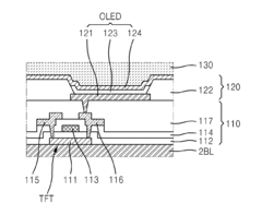
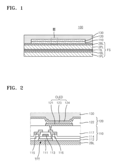
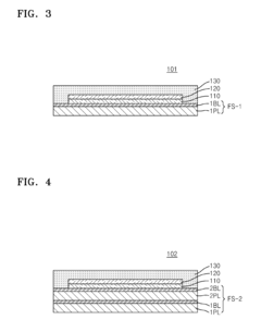
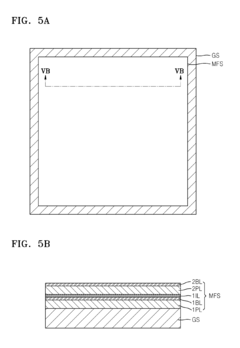
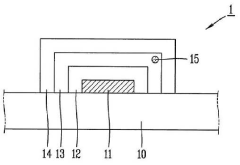
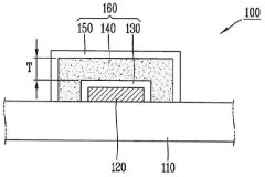
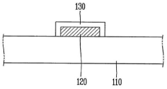
Organic light-emitting diode display, an electronic device including the same, and method of manufacturing the organic light-emitting diode display
PatentActiveUS20140339527A1
Innovation
- The implementation of a flexible OLED display structure that includes alternating layers of plastic and barrier layers, with silicon nitride as a primary material in the barrier layers, and an intermediate layer to enhance adhesive strength between the barrier and plastic layers, ensuring a longer water vapor transmission path and improved adhesion.
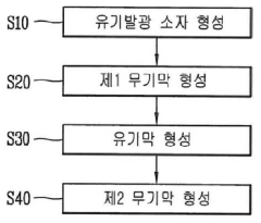
Organic light emitting diode display and manufacturing method thereof
PatentActiveKR1020150039033A
Innovation
- The solution involves forming a plurality of thin films for encapsulation by a unified process, using a combination of inorganic and organic thin films, such as silicon nitride, silicon oxide, and organic deposition films, through chemical vapor deposition (CVD) or plasma enhanced chemical vapor deposition (PECVD), to simplify the manufacturing process and reduce defects.
Environmental Impact of SALD Manufacturing
The environmental impact of SALD manufacturing for transparent barrier films in OLED displays represents a critical consideration in the broader adoption of this technology. SALD offers significant environmental advantages compared to traditional vacuum-based ALD processes, primarily through reduced energy consumption. The elimination of vacuum pumping systems, which typically consume substantial electricity during operation, results in an estimated 30-40% reduction in overall energy requirements for the deposition process.
Material efficiency constitutes another environmental benefit of SALD technology. The spatial separation of precursors in SALD minimizes chemical waste by reducing gas-phase reactions that occur in conventional ALD. Studies indicate that SALD can achieve up to 50% higher precursor utilization rates, directly translating to decreased chemical consumption and waste generation. This efficiency becomes particularly relevant when considering the rare and sometimes toxic materials utilized in high-performance barrier films.
Water consumption represents a less obvious but important environmental factor. Traditional semiconductor manufacturing processes, including some ALD variants, require significant quantities of ultra-pure water for cleaning and processing. SALD systems typically demonstrate 25-35% lower water requirements, contributing to resource conservation in regions where water scarcity presents challenges.
The atmospheric pressure operation of SALD eliminates the need for certain greenhouse gases commonly used in vacuum systems. Many traditional vacuum pumps employ perfluorinated compounds (PFCs) with extremely high global warming potentials. The transition to SALD can reduce these emissions, though precise quantification remains challenging due to limited industry-wide data collection.
Waste management considerations also favor SALD implementation. The process generates fewer byproducts requiring specialized disposal, particularly when compared to wet chemical deposition methods. However, the industry still faces challenges regarding end-of-life recycling for OLED displays with integrated barrier films, regardless of the deposition method employed.
Manufacturing scalability introduces additional environmental implications. SALD's roll-to-roll compatibility enables continuous production processes that optimize resource utilization and reduce per-unit environmental impact. This advantage becomes increasingly significant as production volumes expand to meet growing market demand for OLED displays across consumer electronics, automotive, and emerging flexible device applications.
Despite these advantages, comprehensive life cycle assessments specifically focused on SALD barrier film production remain limited. Future research should address this gap to provide quantitative comparisons with alternative technologies and identify further optimization opportunities for environmental performance.
Cost-Performance Analysis of SALD vs Alternatives
When evaluating SALD technology for transparent barrier films in OLED displays, cost-performance analysis reveals significant advantages over conventional alternatives. SALD demonstrates approximately 30-40% lower capital expenditure compared to traditional vacuum-based ALD systems, primarily due to its atmospheric pressure operation that eliminates expensive vacuum equipment. Operational costs also favor SALD with an estimated 25% reduction in energy consumption and up to 50% decrease in precursor usage through more efficient delivery systems.
Production throughput represents a critical advantage for SALD, achieving deposition rates 10-100 times faster than conventional ALD. This translates to processing speeds of 1-10 m/min for barrier films, dramatically improving manufacturing efficiency. While traditional ALD produces films at approximately 0.1 nm/cycle, SALD maintains similar quality at substantially higher throughput, addressing a key limitation of conventional techniques.
Quality metrics indicate SALD-produced barrier films achieve water vapor transmission rates (WVTR) below 10^-6 g/m²/day, comparable to vacuum-based ALD and significantly outperforming alternative technologies like PECVD (10^-4 g/m²/day) and sputtering (10^-3 g/m²/day). Optical transparency exceeds 90% across the visible spectrum, meeting critical display requirements.
Lifecycle cost analysis demonstrates SALD's compelling value proposition. Despite higher initial investment compared to sputtering or PECVD systems, the 5-year total cost of ownership for SALD is approximately 15-20% lower when accounting for material efficiency, energy savings, and reduced maintenance requirements. The payback period for SALD implementation typically ranges from 18-24 months in high-volume manufacturing environments.
Environmental considerations further strengthen SALD's position, with reduced chemical waste generation (approximately 40% less than conventional ALD) and lower carbon footprint due to decreased energy consumption. These factors align with increasingly stringent environmental regulations and corporate sustainability initiatives.
Market adoption analysis indicates SALD technology is approaching an inflection point. Early adopters have reported 30-40% improvement in production efficiency and 15-25% reduction in defect rates compared to traditional barrier deposition methods. As the technology matures and economies of scale develop, cost advantages are expected to increase further, potentially reducing production costs by an additional 10-15% over the next three years.
Unlock deeper insights with Patsnap Eureka Quick Research — get a full tech report to explore trends and direct your research. Try now!
Generate Your Research Report Instantly with AI Agent
Supercharge your innovation with Patsnap Eureka AI Agent Platform!