Atmospheric ALD For Silver And Copper Thin Film Metallization
AUG 28, 20259 MIN READ
Generate Your Research Report Instantly with AI Agent
Patsnap Eureka helps you evaluate technical feasibility & market potential.
ALD Metallization Background and Objectives
Atomic Layer Deposition (ALD) has emerged as a pivotal technology in the semiconductor industry, offering unprecedented control over thin film deposition at the atomic scale. The evolution of ALD for metallization applications, particularly for silver and copper thin films, represents a significant advancement in microelectronics manufacturing. Traditionally, physical vapor deposition (PVD) and chemical vapor deposition (CVD) have dominated metallization processes, but their limitations in conformality, step coverage, and thickness control have become increasingly problematic as device dimensions continue to shrink.
The development of ALD for metallization can be traced back to the early 2000s, with initial focus on noble metals like platinum and palladium. However, the extension to silver and copper has been challenging due to their unique chemical properties and tendency to agglomerate during deposition. The atmospheric pressure variant of ALD (AP-ALD) represents a further evolution, offering potential advantages in throughput, cost-effectiveness, and integration with roll-to-roll manufacturing processes.
The primary technical objective of atmospheric ALD for silver and copper metallization is to achieve uniform, conformal, and high-quality metal films with excellent electrical conductivity while operating at atmospheric pressure. This approach aims to overcome the vacuum requirements of conventional ALD, which represent significant cost and complexity factors in industrial implementation. Additionally, the technology seeks to enable precise control over film thickness down to sub-nanometer levels, critical for next-generation electronic devices.
Current technological trends indicate a growing interest in spatial ALD configurations for atmospheric processing, where precursors are spatially separated rather than temporally sequenced. This approach potentially offers orders of magnitude higher deposition rates compared to conventional ALD, addressing one of the primary limitations of the technology for industrial adoption.
The broader objectives of this technology development include enabling more efficient manufacturing processes for flexible electronics, photovoltaics, and advanced packaging applications. Silver and copper are particularly valuable target materials due to their superior electrical conductivity, with copper being the industry standard for interconnects and silver offering even lower resistivity for specialized applications.
Successful implementation of atmospheric ALD for silver and copper metallization would represent a significant breakthrough in thin film deposition technology, potentially revolutionizing manufacturing processes for a wide range of electronic devices and enabling new device architectures that are currently constrained by metallization limitations.
Market Analysis for Ag/Cu Thin Film Applications
The global market for silver and copper thin film applications is experiencing robust growth, driven by increasing demand across multiple industries. The thin film metallization market, valued at approximately $2.3 billion in 2022, is projected to reach $3.7 billion by 2028, with a compound annual growth rate of 8.2%. Within this segment, silver and copper thin films represent significant market share due to their superior electrical conductivity and cost-effectiveness compared to alternative materials.
Electronics manufacturing constitutes the largest application segment, accounting for nearly 45% of the total market. The miniaturization trend in consumer electronics has intensified demand for high-performance thin film metallization solutions that can deliver enhanced conductivity while reducing material usage. Particularly, the semiconductor industry's shift toward advanced packaging technologies has created substantial opportunities for atmospheric ALD-based silver and copper thin films.
Renewable energy applications represent the fastest-growing segment, with solar photovoltaics leading the charge. Silver thin films are critical components in high-efficiency solar cells, where their superior conductivity properties directly impact energy conversion rates. The market for silver thin films in solar applications alone is expected to grow at 12.4% annually through 2028, driven by global renewable energy initiatives and declining solar installation costs.
The automotive sector presents another significant growth opportunity, particularly with the accelerating transition to electric vehicles. Advanced battery technologies and power electronics require high-performance metallization solutions that can withstand demanding operational conditions while maintaining optimal electrical performance. Copper thin films are increasingly preferred in this segment due to their cost advantage over silver while maintaining acceptable conductivity levels.
Regional analysis reveals Asia-Pacific as the dominant market, accounting for approximately 58% of global consumption, with China, South Korea, Taiwan, and Japan leading manufacturing capacity. North America and Europe follow with 22% and 17% market share respectively, with particular strength in high-value applications requiring advanced metallization techniques.
The market is also witnessing a shift toward sustainable manufacturing processes, with atmospheric ALD gaining traction due to its reduced environmental footprint compared to traditional vacuum-based deposition methods. This trend aligns with increasing regulatory pressure and corporate sustainability initiatives across major markets, creating additional demand drivers for atmospheric ALD technologies for silver and copper thin film metallization.
Current Challenges in Atmospheric ALD Technology
Despite significant advancements in Atmospheric Atomic Layer Deposition (AALD) for silver and copper thin film metallization, several critical challenges continue to impede widespread industrial adoption. The foremost challenge lies in achieving precise control over film uniformity and thickness across large substrate areas. Unlike vacuum-based ALD, atmospheric conditions introduce additional variables such as gas flow dynamics, ambient contaminants, and pressure fluctuations that can compromise the self-limiting nature of ALD reactions.
Precursor chemistry presents another substantial hurdle. Current silver and copper precursors often exhibit insufficient volatility or thermal stability under atmospheric conditions, leading to premature decomposition or inadequate surface saturation. This results in non-ideal growth behavior, including island formation rather than the desired continuous film growth, particularly during early deposition cycles.
Surface oxidation of copper and silver remains problematic in atmospheric environments. The high reactivity of these metals with ambient oxygen necessitates sophisticated precursor design and process optimization to prevent oxide formation during deposition. This challenge is particularly acute for copper, which oxidizes more readily than silver under atmospheric conditions.
Nucleation behavior constitutes a significant technical barrier, especially on dielectric or polymer substrates commonly used in flexible electronics. Both silver and copper exhibit poor wetting characteristics on these surfaces, requiring specialized nucleation enhancement strategies such as functionalization layers or nucleation promoters to achieve continuous thin films at low thicknesses.
Scalability and throughput limitations hinder commercial viability. While AALD offers advantages in terms of equipment simplicity compared to vacuum ALD, current deposition rates remain too slow for high-volume manufacturing applications. Typical growth rates of 0.5-1.5 Å per cycle translate to extended process times for achieving films of practical thickness (50-200 nm).
Integration challenges with existing manufacturing processes further complicate adoption. AALD equipment must be compatible with roll-to-roll processing for flexible electronics or in-line processing for semiconductor applications, requiring careful engineering of gas delivery systems, temperature management, and substrate handling mechanisms.
Environmental and safety concerns associated with metal-organic precursors used in AALD processes demand attention. Many silver and copper precursors contain toxic or environmentally harmful components, necessitating robust containment and waste management systems, particularly challenging in open atmospheric systems compared to closed vacuum chambers.
Existing Atmospheric ALD Technical Solutions
01 Atmospheric ALD techniques for silver thin films
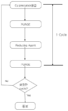
Atmospheric Atomic Layer Deposition (ALD) can be used to deposit silver thin films for metallization applications. This process involves sequential exposure of the substrate to silver precursors and reducing agents at atmospheric pressure, allowing for controlled growth of silver films with excellent uniformity and conformality. The technique enables low-temperature deposition of silver films with high purity and good adhesion properties, making it suitable for various electronic applications.- Atmospheric pressure ALD for silver thin films: Atmospheric pressure atomic layer deposition (ALD) techniques for depositing silver thin films on substrates. These methods involve sequential exposure of the substrate to silver precursors and reducing agents under atmospheric conditions, allowing for precise control of film thickness and uniformity. The process enables low-temperature deposition of silver films with excellent adhesion and electrical conductivity properties, making it suitable for various electronic applications.
- Copper thin film deposition using ALD at atmospheric conditions: Methods for depositing copper thin films using atomic layer deposition at atmospheric pressure. These techniques utilize specific copper precursors and reactants in alternating exposure cycles to achieve controlled growth of copper films. The atmospheric pressure conditions eliminate the need for complex vacuum systems, reducing manufacturing costs while maintaining high-quality film properties. The resulting copper films exhibit excellent electrical conductivity and can be used in semiconductor interconnects and other electronic components.
- Precursor chemistry for metal ALD processes: Development of specialized precursors for silver and copper atomic layer deposition. These precursors are designed to have appropriate volatility, reactivity, and thermal stability for effective use in atmospheric pressure ALD processes. The chemistry involves organometallic compounds that can react selectively with surfaces to form metallic films while producing volatile byproducts that are easily removed. Optimization of precursor delivery systems and reaction parameters ensures uniform film growth with minimal impurities.
- Equipment and reactor design for atmospheric ALD: Specialized equipment and reactor designs for performing atmospheric pressure atomic layer deposition of silver and copper films. These systems include precursor delivery mechanisms, reaction chambers with controlled gas flow patterns, and temperature management systems. The reactors are designed to enable rapid gas switching while preventing premature reactions between precursors. Some designs incorporate spatial ALD concepts where the substrate moves between different reaction zones, enabling high-throughput continuous processing for industrial applications.
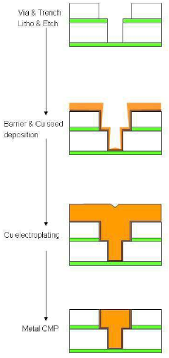
- Applications and integration of ALD metal films: Integration of atmospherically deposited silver and copper thin films into various device structures and applications. These applications include interconnects for semiconductor devices, transparent conductive electrodes, plasmonic structures, and catalytic surfaces. The ALD process allows for conformal coating on complex 3D structures and enables precise thickness control needed for advanced electronic devices. Post-deposition treatments such as annealing can further enhance the electrical and mechanical properties of the metal films for specific applications.
02 Copper thin film deposition using atmospheric ALD
Atmospheric pressure Atomic Layer Deposition can be employed for depositing copper thin films with precise thickness control. The process typically uses copper precursors such as copper(I) compounds or copper(II) β-diketonates along with reducing agents to achieve layer-by-layer growth at atmospheric conditions. This approach offers advantages including lower equipment costs compared to vacuum-based methods, while maintaining excellent step coverage and film quality for metallization applications in semiconductor devices.Expand Specific Solutions03 Precursors and reactants for metal ALD processes
Selection of appropriate precursors and reactants is crucial for successful atmospheric ALD of silver and copper thin films. Metal-organic compounds, halides, and β-diketonates serve as effective metal sources, while hydrogen, plasma, or organic reducing agents function as second reactants. The precursors must exhibit sufficient volatility at atmospheric pressure, thermal stability during delivery, and high reactivity with the substrate surface to ensure complete and self-limiting reactions for uniform film growth.Expand Specific Solutions04 Equipment and reactor designs for atmospheric ALD
Specialized reactor designs are essential for atmospheric ALD of silver and copper films. These systems typically feature spatial separation of precursors using inert gas barriers, precise gas flow control, and temperature management systems. Reactor configurations include flow-type reactors, rotating substrate systems, and roll-to-roll designs for continuous processing. These equipment innovations enable efficient precursor utilization, prevent premature gas-phase reactions, and allow for scalable production of high-quality metal thin films without vacuum requirements.Expand Specific Solutions05 Applications and integration of ALD metal films
Atmospheric ALD-deposited silver and copper thin films find applications in various technological fields. These include interconnects in microelectronics, seed layers for electroplating, transparent conductive electrodes, plasmonic devices, and catalytic surfaces. The integration of these films into device fabrication processes requires consideration of adhesion layers, post-deposition treatments, and compatibility with subsequent processing steps. The atmospheric deposition approach enables cost-effective metallization solutions for flexible electronics, solar cells, and other emerging technologies.Expand Specific Solutions
Leading Companies in ALD Metallization Industry
The atmospheric ALD for silver and copper thin film metallization market is currently in a growth phase, driven by increasing demand for advanced semiconductor and electronic components. The market size is expanding rapidly, with projections indicating significant growth due to the technology's applications in microelectronics, photovoltaics, and emerging IoT devices. From a technical maturity perspective, the field is transitioning from developmental to commercial implementation, with key players demonstrating varying levels of expertise. Industry leaders like Applied Materials, ASM International, and Samsung Electronics have established strong positions through advanced R&D capabilities, while specialized firms such as Beneq Group and Picosun Oy offer targeted solutions. Academic-industrial partnerships involving institutions like Harvard College and CNRS are accelerating innovation, particularly in addressing challenges related to adhesion, uniformity, and integration with existing manufacturing processes.
ASM International NV
Technical Solution: ASM International has developed advanced Atmospheric Atomic Layer Deposition (AALD) technology for silver and copper thin film metallization, focusing on their ALD XP8 and Synergis platforms. Their approach utilizes plasma-enhanced ALD processes operating at atmospheric pressure, which enables direct integration into existing manufacturing lines without vacuum requirements. For silver deposition, they employ organometallic precursors like silver beta-diketonates combined with oxygen-containing reactants, achieving film thicknesses of 5-50nm with resistivity approaching bulk values (1.6-2.0 μΩ·cm). For copper, they've pioneered a three-step process using Cu(hfac)(vtms) precursors with controlled nucleation phases, resulting in continuous films at thicknesses below 10nm. Their technology incorporates in-situ surface preparation steps to enhance adhesion on various substrates including silicon, glass, and polymers, while maintaining deposition rates of approximately 0.5-1.0Å per cycle. ASM's solution also features real-time monitoring systems that ensure precise thickness control and uniformity across 300mm wafers with <2% variation.
Strengths: Superior film quality with near-bulk conductivity values; excellent step coverage in high-aspect-ratio features (>95% in 10:1 structures); compatibility with temperature-sensitive substrates through low thermal budget processes (80-150°C). Weaknesses: Relatively slower deposition rates compared to PVD techniques; higher precursor costs than conventional metallization methods; potential challenges with precursor volatility control in atmospheric conditions.
Applied Materials, Inc.
Technical Solution: Applied Materials has developed a comprehensive Atmospheric ALD solution for silver and copper metallization called the "Endura® AtmoSync™" platform. This technology employs a spatial ALD approach where substrates move continuously through separated reaction zones maintained at atmospheric pressure. For silver deposition, they utilize silver carboxylate precursors (Ag(O₂CR)) combined with hydrogen plasma treatment, achieving growth rates of approximately 0.8-1.2Å per cycle while maintaining film resistivity below 2.5 μΩ·cm. Their copper process incorporates a novel dual-precursor strategy using Cu(dmap)₂ and Cu(hfac)(vtms) with controlled oxidation-reduction cycles, enabling conformal deposition in features with aspect ratios exceeding 15:1. The system includes proprietary gas delivery systems that precisely control precursor dosing and separation, preventing gas-phase reactions while maintaining atmospheric conditions. Applied Materials' solution also features integrated pre-treatment modules that modify substrate surfaces with self-assembled monolayers to enhance nucleation density, particularly important for noble metals like silver that typically exhibit island growth. Their process achieves film closure at thicknesses as low as 5-7nm, significantly lower than conventional PVD methods requiring 15-20nm for continuous films.
Strengths: Industry-leading throughput (>100 wafers/hour) while maintaining excellent film quality; superior conformality in complex 3D structures; integrated metrology for real-time process control; reduced capital costs compared to vacuum-based systems. Weaknesses: Higher precursor consumption compared to vacuum ALD; potential challenges with precursor volatility control in atmospheric conditions; more complex gas flow management requirements to prevent parasitic reactions.
Key Innovations in Ag/Cu Precursor Chemistry
Atomic layer deposition of copper using surface-activating agents
PatentInactiveEP1791988A2
Innovation
- The process involves introducing a surface-activating agent to form a monolayer on the substrate, followed by a copper precursor and a reducing agent, allowing for self-limiting adsorption and thermal stability, avoiding thermal degradation and enabling the formation of high-quality, uniform copper films at lower temperatures.
Method of deposition of metal thin film by using atomic layer deposition
PatentInactiveKR1020100013832A
Innovation
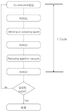
- A method involving atomic layer deposition (ALD) using copper precursors and nitriding or oxidizing agents followed by reducing agents, with controlled plasma and gas environments, to form copper thin films with excellent adhesion and density on various substrates without requiring subsequent heat treatment.
Environmental Impact Assessment of ALD Processes
The environmental impact of Atmospheric Atomic Layer Deposition (ALD) processes for silver and copper thin film metallization requires comprehensive assessment due to the growing importance of sustainable manufacturing in the electronics industry. Atmospheric ALD offers significant environmental advantages over traditional vacuum-based deposition methods, primarily through reduced energy consumption by eliminating the need for high-vacuum environments.
The precursor chemistry used in silver and copper ALD processes presents both challenges and opportunities from an environmental perspective. Metal-organic precursors commonly employed for these metals often contain volatile organic compounds (VOCs) that may contribute to air pollution if not properly managed. However, the precise nature of ALD allows for extremely efficient precursor utilization, with theoretical material efficiency approaching 100% compared to physical vapor deposition methods that typically waste 70-90% of target materials.
Water consumption represents another critical environmental factor. Atmospheric ALD processes generally require less cooling water than vacuum-based systems, as they operate at lower temperatures and don't need extensive vacuum pump cooling. This advantage becomes particularly significant in regions facing water scarcity challenges, where manufacturing water footprint is increasingly scrutinized.
Waste stream analysis reveals that atmospheric ALD generates minimal solid waste compared to wet chemical processes like electroplating, which produce substantial quantities of metal-contaminated effluent requiring treatment. The primary waste outputs from ALD are unreacted precursors and byproducts, which can be effectively captured and neutralized using modern abatement systems.
Life cycle assessment (LCA) studies comparing atmospheric ALD with conventional metallization techniques demonstrate favorable outcomes for ALD in terms of global warming potential and resource depletion metrics. The extended equipment lifespan and reduced maintenance requirements of atmospheric systems further enhance their environmental profile when considering manufacturing infrastructure impacts.
Regulatory compliance considerations are increasingly important as environmental legislation tightens globally. Atmospheric ALD processes for silver and copper typically use less restricted chemicals than electroplating, which often relies on cyanide-based chemistries and strong acids. This positions atmospheric ALD favorably as regulations on hazardous substances continue to evolve, particularly in regions like the European Union with stringent chemical management frameworks.
Future environmental optimization pathways for atmospheric ALD include developing greener precursors with lower toxicity profiles, implementing closed-loop precursor recycling systems, and integrating renewable energy sources to power deposition equipment. These advancements could further reduce the already favorable environmental footprint of atmospheric ALD for silver and copper metallization applications.
Cost-Benefit Analysis of Atmospheric vs. Vacuum ALD
The economic comparison between atmospheric and vacuum ALD processes for silver and copper metallization reveals significant cost differentials across multiple operational dimensions. Initial capital expenditure for atmospheric ALD systems typically ranges 30-40% lower than vacuum-based counterparts, primarily due to the elimination of complex vacuum chambers and associated pumping systems. This reduced hardware complexity translates to smaller cleanroom footprint requirements, further decreasing facility costs.
Operational expenses show even more dramatic differences. Energy consumption in atmospheric systems is approximately 45-55% lower, as they eliminate the substantial power demands of vacuum generation and maintenance. Atmospheric ALD also demonstrates 25-35% faster processing cycles by removing vacuum pump-down time between deposition cycles, significantly enhancing throughput capabilities for high-volume manufacturing environments.
Maintenance costs favor atmospheric systems with 20-30% lower annual expenditures. The absence of vacuum pumps, seals, and related components reduces both scheduled maintenance frequency and the complexity of service interventions. This translates to higher equipment availability and reduced production interruptions.
However, atmospheric ALD systems face challenges in precursor efficiency. The open-air environment typically results in 15-25% higher precursor consumption compared to vacuum systems, where reactive chemicals are more contained. This difference becomes particularly significant when working with expensive silver precursors, partially offsetting other operational savings.
Film quality considerations introduce additional cost implications. While atmospheric ALD can achieve comparable film quality for many applications, ultra-high-purity requirements may necessitate additional process optimization or post-deposition treatments, potentially adding 5-15% to process costs for the most demanding applications.
The total cost of ownership analysis indicates atmospheric ALD provides 20-30% overall cost reduction for standard metallization applications. This advantage becomes more pronounced in high-throughput manufacturing scenarios where the faster cycle times and reduced energy consumption compound over production volume. For specialized applications requiring exceptional film purity or ultra-precise thickness control, the cost advantage narrows but typically remains favorable for atmospheric processes when considering the complete production lifecycle.
Unlock deeper insights with Patsnap Eureka Quick Research — get a full tech report to explore trends and direct your research. Try now!
Generate Your Research Report Instantly with AI Agent
Supercharge your innovation with Patsnap Eureka AI Agent Platform!