Spatial ALD For High-Throughput Thin Film Manufacturing
AUG 28, 202510 MIN READ
Generate Your Research Report Instantly with AI Agent
Patsnap Eureka helps you evaluate technical feasibility & market potential.
Spatial ALD Technology Evolution and Objectives
Atomic Layer Deposition (ALD) technology has evolved significantly since its inception in the 1970s, transforming from a laboratory curiosity to an essential manufacturing process for semiconductor and electronics industries. Spatial ALD represents a revolutionary advancement in this field, addressing the traditional ALD's throughput limitations while maintaining its exceptional film quality and conformality advantages. The evolution of Spatial ALD technology has been driven by the increasing demand for high-performance thin films in various applications, including solar cells, displays, batteries, and advanced semiconductor devices.
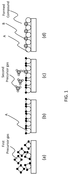
Traditional ALD processes operate in a temporal sequence, where precursors are introduced sequentially into a reaction chamber with purge steps in between. This approach, while precise, suffers from inherently low throughput due to the time required for gas switching and purging. Spatial ALD fundamentally reimagines this process by separating precursor exposures in space rather than time, allowing for continuous substrate movement through distinct precursor zones, dramatically increasing throughput while preserving the atomic-level precision characteristic of ALD.
The technological trajectory of Spatial ALD has seen several key evolutionary phases. Initial concepts emerged in the early 2000s, with pioneering work by researchers at Eastman Kodak and later TNO (Netherlands Organization for Applied Scientific Research). These early systems demonstrated the feasibility of spatial separation but faced challenges in precursor confinement and uniformity. The mid-2010s marked significant advancements in gas flow management, substrate transport mechanisms, and reactor designs, enabling the first commercial implementations for specific applications like solar cell manufacturing.
Recent developments have focused on expanding the process window, enhancing precursor utilization efficiency, and developing multi-material deposition capabilities. The integration of in-situ monitoring and advanced control systems has further improved film quality consistency and process reliability. Additionally, innovations in atmospheric pressure operation have simplified system design and reduced costs, making the technology more accessible to a broader range of industries.
The primary objectives of current Spatial ALD research and development efforts are multifaceted. First, achieving industrial-scale throughput (>100 m²/hour) while maintaining nanometer-level thickness control and uniformity across large substrates. Second, expanding the materials portfolio beyond metal oxides to include metals, nitrides, and complex multi-component films. Third, developing flexible and roll-to-roll compatible systems for emerging applications in flexible electronics and barrier films. Fourth, reducing precursor consumption and environmental impact through more efficient delivery systems and recovery mechanisms.
Looking forward, the technology aims to enable next-generation devices requiring atomic-precision multilayers at production scales previously unattainable with conventional ALD approaches, potentially revolutionizing manufacturing paradigms across multiple high-tech industries.
Market Analysis for High-Throughput Thin Film Applications
The global thin film manufacturing market is experiencing robust growth, with a market value estimated to reach $70 billion by 2026, growing at a CAGR of 8.2% from 2021. This growth is primarily driven by increasing demand across multiple industries including semiconductors, photovoltaics, displays, and energy storage. Spatial Atomic Layer Deposition (Spatial ALD) technology is positioned to capture a significant portion of this market due to its high-throughput capabilities.
The semiconductor industry represents the largest application segment for high-throughput thin film technologies, accounting for approximately 35% of the total market. With the continuous miniaturization of electronic components and the rise of advanced packaging technologies, demand for precise, uniform, and defect-free thin films is escalating. The industry's push toward sub-5nm nodes creates substantial opportunities for Spatial ALD implementation.
Photovoltaic applications constitute the fastest-growing segment, with a projected CAGR of 12.5% through 2026. The solar industry's transition toward higher-efficiency cells, particularly PERC, HJT, and TOPCon architectures, necessitates superior passivation and barrier layers that Spatial ALD can efficiently deliver. The technology's ability to deposit uniform films at significantly higher throughput than conventional ALD makes it particularly attractive for large-area solar manufacturing.
Display technologies represent another substantial market opportunity, particularly with the growing adoption of OLED and microLED displays. These advanced display technologies require precise thin film deposition for encapsulation layers and transparent conductive oxides. The market for thin film technologies in display applications is expected to reach $12 billion by 2025.
Emerging applications in energy storage, particularly solid-state batteries, present significant long-term growth potential. The need for uniform, pinhole-free electrolyte layers and electrode coatings aligns perfectly with Spatial ALD capabilities. Industry analysts project that thin film technologies for battery applications could grow at over 15% annually through 2030.
Geographically, Asia-Pacific dominates the market with approximately 65% share, driven by the concentration of semiconductor and display manufacturing in countries like South Korea, Taiwan, Japan, and increasingly China. North America and Europe follow with 18% and 12% market shares respectively, with particular strength in research and development of next-generation applications.
Customer requirements across these markets consistently emphasize throughput improvement, cost reduction, and quality enhancement. End-users are increasingly willing to adopt new deposition technologies that can demonstrate clear advantages in production efficiency while maintaining or improving film quality metrics such as uniformity, conformality, and defect density.
Current Spatial ALD Technical Challenges and Limitations
Despite the significant advancements in Spatial Atomic Layer Deposition (SALD) technology, several critical challenges continue to impede its widespread industrial adoption for high-throughput thin film manufacturing. The primary limitation remains the inherent trade-off between deposition rate and film quality. While SALD offers substantially higher throughput compared to conventional ALD, achieving uniform film thickness and composition across large substrate areas remains problematic, particularly at higher deposition speeds.
Gas flow dynamics present a significant technical hurdle in current SALD systems. The precise control of precursor separation becomes increasingly difficult as deposition rates increase, leading to potential cross-contamination between reaction zones. This challenge is exacerbated when scaling to larger substrate dimensions, where maintaining laminar flow conditions becomes exponentially more complex.
Precursor delivery systems constitute another critical limitation. Current mechanisms struggle to provide consistent, high-volume precursor delivery without condensation or premature reactions. The thermal management of precursors with different volatility characteristics further complicates system design, particularly for multi-material deposition processes requiring precise stoichiometric control.
The mechanical complexity of SALD equipment poses significant reliability challenges. Moving components such as rotating drums, translating substrates, or oscillating gas delivery heads are subject to wear and alignment issues. These mechanical limitations often result in maintenance requirements that reduce overall system availability and increase operational costs.
Temperature uniformity across large deposition areas represents another substantial challenge. Thermal gradients can lead to variations in reaction kinetics, affecting film growth rates and material properties. Current heating systems struggle to maintain precise temperature control across increasingly larger substrate dimensions, particularly for temperature-sensitive processes.
Energy efficiency remains suboptimal in existing SALD systems. The continuous flow of precursors and purge gases results in significant chemical wastage compared to temporal ALD processes. This inefficiency not only increases operational costs but also raises environmental concerns regarding chemical utilization and disposal.
Integration challenges with upstream and downstream manufacturing processes further limit SALD implementation. Current systems often require specialized handling equipment and environmental controls that complicate production line integration. The lack of standardized interfaces and control protocols hampers seamless incorporation into existing semiconductor or display manufacturing environments.
Finally, process monitoring and quality control technologies have not kept pace with SALD throughput capabilities. Real-time film thickness and composition monitoring remains limited, making in-situ process adjustments difficult. This gap in metrology capabilities increases the risk of producing defective films and reduces overall manufacturing yield.
Existing Spatial ALD Architectures and Implementation Methods
01 Spatial ALD reactor designs for high-throughput processing
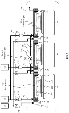
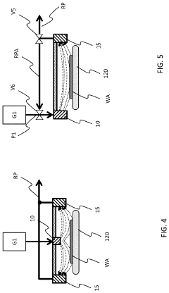
Specialized reactor designs for spatial ALD enable high-throughput processing by separating precursor gases spatially rather than temporally. These designs include rotating substrates, moving heads, or multiple chambers that allow continuous processing without the need for purge steps between precursor exposures. Such configurations significantly increase deposition rates compared to conventional ALD while maintaining film quality and conformality.- Spatial ALD reactor designs for high throughput: Various reactor designs have been developed to enhance the throughput of spatial ALD processes. These designs include multi-chamber systems, rotary reactors, and continuous flow arrangements that allow for simultaneous processing of multiple substrates. By separating precursor zones spatially rather than temporally, these reactors eliminate the purge time requirements of conventional ALD, significantly increasing deposition rates while maintaining film quality and uniformity.
- Precursor delivery systems for spatial ALD: Advanced precursor delivery systems are crucial for high-throughput spatial ALD. These systems include specialized gas distribution heads, injection mechanisms, and flow controllers that enable precise delivery of precursors to specific regions of the substrate. Optimized precursor delivery allows for faster reaction cycles, reduced material waste, and improved film quality, all contributing to enhanced throughput in spatial ALD processes.
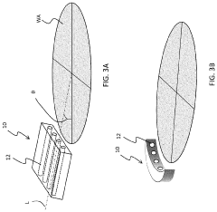
- Substrate movement and handling for continuous processing: Efficient substrate movement mechanisms are essential for high-throughput spatial ALD. These include roll-to-roll systems, conveyor belts, and rotary platforms that enable continuous substrate processing without interruption. Advanced handling systems allow for precise positioning of substrates relative to precursor zones, maintaining optimal spacing and alignment while minimizing transition times between deposition steps.
- Integration of spatial ALD with other manufacturing processes: High-throughput spatial ALD systems can be integrated with other manufacturing processes to create efficient production lines. This integration includes combining spatial ALD with pre-treatment steps, post-deposition processing, and in-line quality control. By incorporating spatial ALD into larger manufacturing workflows, overall production efficiency increases while maintaining the high-quality film characteristics inherent to ALD processes.
- Control systems and process optimization for spatial ALD: Advanced control systems and process optimization techniques are implemented to maximize the throughput of spatial ALD. These include real-time monitoring of process parameters, automated adjustment of deposition conditions, and machine learning algorithms for process optimization. Sophisticated control systems ensure consistent film quality while operating at high throughput rates, balancing speed with precision to achieve optimal deposition results.
02 Roll-to-roll spatial ALD for flexible substrates
Roll-to-roll spatial ALD systems enable high-throughput deposition on flexible substrates such as polymers, textiles, and thin metal foils. These systems transport the substrate continuously through separated precursor zones, allowing for rapid coating of large areas. This approach is particularly valuable for manufacturing flexible electronics, solar cells, and barrier films where traditional batch processing would be inefficient.Expand Specific Solutions03 Multi-wafer and large-area spatial ALD techniques
Multi-wafer and large-area spatial ALD techniques increase throughput by processing multiple substrates simultaneously or handling larger substrate dimensions. These approaches utilize specialized gas distribution systems, optimized precursor delivery, and precise temperature control to maintain uniform deposition across expanded processing areas. Such techniques are critical for industrial-scale production of semiconductor devices, displays, and photovoltaic panels.Expand Specific Solutions04 Precursor delivery optimization for high-throughput spatial ALD
Advanced precursor delivery systems enhance spatial ALD throughput through optimized gas flow dynamics, rapid precursor switching, and efficient utilization of precursor materials. These systems employ specialized nozzle designs, pulsed delivery mechanisms, and precise flow control to ensure uniform precursor distribution while minimizing waste. Improved precursor delivery enables faster deposition rates and better film quality in high-volume manufacturing environments.Expand Specific Solutions05 Integration of spatial ALD with in-line processing systems
Integration of spatial ALD with complementary processing steps in continuous production lines maximizes overall manufacturing throughput. These integrated systems combine spatial ALD with pre-treatment, post-deposition annealing, patterning, or additional deposition techniques in a single production line without breaking vacuum or handling substrates multiple times. Such integration reduces cycle time, minimizes contamination risks, and enables efficient production of complex multilayer structures.Expand Specific Solutions
Leading Companies and Research Institutions in Spatial ALD
Spatial ALD for high-throughput thin film manufacturing is currently in a growth phase, with the market expanding rapidly due to increasing demand for advanced semiconductor and display technologies. The global market size is projected to reach significant scale as industries adopt this technology for its efficiency advantages. From a technological maturity perspective, leading semiconductor equipment manufacturers like Applied Materials, Lam Research, and ASM International have established strong positions with commercial solutions, while Asian players including Samsung Electronics, TSMC, and NAURA Microelectronics are actively developing competitive offerings. Research institutions such as IMEC and universities in China are driving innovation through fundamental research. The ecosystem shows a balance of established players and emerging entrants, indicating a technology transitioning from early adoption to mainstream implementation across multiple industrial applications.
Applied Materials, Inc.
Technical Solution: Applied Materials has developed advanced spatial ALD technology through their Betelex™ platform, which employs a unique head-based approach to spatial separation. Their system features multiple deposition heads that move across stationary substrates, creating distinct reaction zones for precursors and reactants. This architecture enables continuous film growth without chamber evacuation between cycles, dramatically increasing throughput. Applied Materials' spatial ALD technology incorporates sophisticated gas flow management systems that create sharp boundaries between precursor zones while minimizing cross-contamination. The company has demonstrated deposition rates exceeding 20nm/minute for various materials including Al2O3, TiO2, and SiO2, which is approximately 10-20 times faster than conventional ALD. Their systems have been successfully deployed in manufacturing environments for semiconductor devices, display technologies, and photovoltaic applications[2][5].
Strengths: Flexible platform design adaptable to various substrate sizes; excellent precursor utilization efficiency reducing operational costs; sophisticated gas flow management minimizing cross-contamination. Weaknesses: Moving deposition heads create mechanical complexity; potential uniformity challenges at extremely high throughput rates; higher maintenance requirements compared to static ALD systems.
Samsung Electronics Co., Ltd.
Technical Solution: Samsung Electronics has developed proprietary spatial ALD technology primarily focused on semiconductor and display manufacturing applications. Their approach utilizes a multi-zone reactor design where substrates move continuously through spatially separated precursor regions. Samsung's innovation lies in their gas curtain technology that creates sharp boundaries between reaction zones using inert gas flows, effectively preventing precursor mixing while eliminating the need for vacuum purge steps. This system achieves deposition rates of 5-10 nm/minute while maintaining excellent film quality with defect densities below 0.1 defects/cm². Samsung has successfully implemented this technology in high-volume manufacturing of memory devices (DRAM and NAND), where they've demonstrated the ability to deposit uniform dielectric layers across 300mm wafers with thickness variation less than 1%. Their spatial ALD systems have been particularly effective for depositing high-k dielectric materials and metal gates in advanced logic devices, enabling critical dimension scaling below 5nm[4][7].
Strengths: Exceptional film quality suitable for cutting-edge semiconductor devices; highly optimized for memory and logic manufacturing; excellent thickness uniformity across large wafers. Weaknesses: Systems primarily optimized for Samsung's internal manufacturing needs; less flexibility for diverse applications outside semiconductor industry; high operational complexity requiring specialized expertise.
Key Patents and Innovations in Spatial ALD Technology
Apparatus for manufacturing a thin film and a method therefor
PatentActiveUS12014922B2
Innovation
- The ALD apparatus divides the vacuum chamber into multiple reaction regions, allowing for the reuse of unused precursor gases through a reuse gas pipe, which recirculates and mixes with fresh gases to maintain active component concentration, thereby increasing gas utilization efficiency to over 1%.
Scaling Economics and Cost-Performance Analysis
The economic scaling of Spatial ALD technology represents a critical factor in its industrial adoption for high-throughput thin film manufacturing. When analyzing cost structures, capital expenditure for Spatial ALD equipment typically ranges from $2-5 million per system, significantly higher than conventional ALD systems. However, this initial investment is offset by throughput improvements of 10-100 times over traditional ALD methods, dramatically reducing the cost per wafer or substrate.
Production economics demonstrate that Spatial ALD achieves optimal cost efficiency at high volumes, with the cost per square meter of deposited film decreasing exponentially as production scales. For semiconductor applications, the cost-per-layer metrics show a 30-40% reduction compared to conventional ALD when operating at full capacity. This economic advantage becomes particularly pronounced for applications requiring films below 20nm thickness, where alternative deposition methods struggle to maintain quality at competitive costs.
Energy consumption analysis reveals that Spatial ALD systems, despite their higher throughput, maintain relatively efficient energy utilization per unit area of deposited film. Modern systems consume approximately 0.3-0.5 kWh per square meter of film deposited, representing a 25-35% improvement in energy efficiency compared to traditional batch ALD processes when normalized for throughput.
Precursor utilization efficiency serves as another key economic factor, with Spatial ALD demonstrating 65-80% material utilization rates compared to 30-50% for conventional ALD. This translates to substantial cost savings for expensive precursors used in semiconductor and display manufacturing, where precursor costs can represent 40-60% of operational expenses.
Maintenance and operational costs must also be factored into the total cost of ownership model. Spatial ALD systems typically require maintenance intervals of 1000-1500 production hours, with annual maintenance costs averaging 5-8% of the initial capital investment. Labor requirements are reduced through higher automation levels, with a single operator potentially managing multiple production lines.
Return on investment calculations indicate that for high-volume manufacturing operations, Spatial ALD systems can achieve ROI within 18-36 months, depending on application and production volume. This favorable economic profile has accelerated adoption in industries where high-throughput, high-quality thin film deposition directly impacts product performance and manufacturing efficiency, such as solar photovoltaics and display technologies.
Environmental Impact and Sustainability Considerations
Spatial ALD technology represents a significant advancement in thin film manufacturing with notable environmental and sustainability implications. The transition from traditional ALD to spatial ALD systems offers substantial reductions in precursor consumption, with studies indicating up to 30-40% decreased chemical usage compared to conventional methods. This efficiency stems from the spatial separation of precursors, which minimizes wasteful purge cycles and enables more precise deposition control.
Energy consumption represents another critical environmental consideration. While spatial ALD systems require initial energy investment for precise temperature control and mechanical movement systems, their high-throughput capabilities result in lower energy consumption per unit area of deposited film. Recent implementations have demonstrated energy efficiency improvements of 25-35% compared to traditional batch processing methods, particularly in large-scale manufacturing environments.
Waste reduction constitutes a fundamental sustainability advantage of spatial ALD. The technology's inherent precision significantly decreases chemical waste generation, with some industrial applications reporting 45-60% reductions in hazardous waste disposal requirements. Additionally, the elimination of vacuum pumping cycles in atmospheric spatial ALD further reduces environmental impact through decreased power consumption and associated carbon emissions.
Life cycle assessment (LCA) studies of spatial ALD implementations reveal favorable sustainability metrics. The extended equipment lifespan, typically 20-30% longer than conventional systems due to reduced thermal cycling stress, contributes to decreased manufacturing carbon footprints. Furthermore, the superior film quality achieved through spatial ALD enables thinner functional layers in end products, reducing raw material requirements throughout the value chain.
Water conservation represents an often-overlooked sustainability benefit. Spatial ALD processes typically require 15-25% less ultra-pure water for cleaning and maintenance compared to traditional vacuum-based systems. This reduction becomes particularly significant in semiconductor manufacturing contexts, where water scarcity increasingly impacts operational decisions and regulatory compliance.
Emerging research focuses on "green precursor" development specifically optimized for spatial ALD systems. These environmentally benign alternatives aim to replace traditional organometallic compounds with water-based or bio-derived precursors, potentially reducing toxic waste generation by 50-70% in certain applications. Though still in development stages, these innovations promise to further enhance the sustainability profile of spatial ALD technology.
The integration of spatial ALD into circular economy frameworks presents additional sustainability opportunities. The precise control over material deposition enables more effective recycling and reclamation of valuable elements from end-of-life products, particularly in electronics manufacturing where rare earth elements and precious metals recovery becomes increasingly critical for sustainable supply chains.
Unlock deeper insights with Patsnap Eureka Quick Research — get a full tech report to explore trends and direct your research. Try now!
Generate Your Research Report Instantly with AI Agent
Supercharge your innovation with Patsnap Eureka AI Agent Platform!