APALD For Photoelectrode Protection In Photoelectrochemical Cells
AUG 28, 202510 MIN READ
Generate Your Research Report Instantly with AI Agent
Patsnap Eureka helps you evaluate technical feasibility & market potential.
APALD Technology Background and Objectives
Atomic Layer Deposition (ALD) has emerged as a pivotal thin-film deposition technique since its development in the 1970s, with significant advancements occurring in the 1990s. The evolution to Atmospheric Pressure Atomic Layer Deposition (APALD) represents a crucial technological leap, eliminating the need for vacuum systems while maintaining precise atomic-level control over film growth. This innovation has dramatically reduced equipment costs and complexity, making the technology more accessible for industrial applications.
APALD technology has gained particular attention in the field of photoelectrochemical (PEC) cells, where protecting photoelectrodes from corrosion and degradation remains a critical challenge. Traditional PEC systems suffer from limited durability due to the harsh electrochemical environment, significantly hampering their commercial viability and widespread adoption for renewable energy applications such as solar water splitting and CO2 reduction.
The historical trajectory of protective coatings for photoelectrodes has progressed from simple metal oxide layers to more sophisticated multi-layer architectures. Early attempts using conventional deposition methods often resulted in pinholes and non-uniform coverage, leading to premature device failure. APALD offers unprecedented conformality and thickness precision at the nanometer scale, even on complex three-dimensional structures, addressing these fundamental limitations.
Recent technological advancements have focused on developing APALD processes compatible with temperature-sensitive photoelectrode materials, expanding the range of applicable substrates. The ability to deposit high-quality protective films at lower temperatures (below 200°C) represents a significant breakthrough, enabling integration with organic and hybrid photoactive materials that would otherwise degrade under conventional processing conditions.
The primary objective of APALD for photoelectrode protection is to develop ultrathin (typically 5-50 nm) conformal coatings that simultaneously provide chemical stability in aggressive electrolytes while maintaining efficient charge transfer between the photoelectrode and the electrolyte. These coatings must exhibit minimal optical absorption to ensure maximum light harvesting by the underlying photoactive material.
Secondary objectives include scaling APALD processes for large-area deposition to enable commercial manufacturing, reducing deposition times through process optimization, and developing multi-component films with tailored properties such as catalytic activity and selective ion permeability. The ultimate goal is to extend photoelectrode operational lifetimes from hours to years, making PEC systems economically viable for renewable energy production.
The technology evolution trend points toward spatial APALD systems capable of continuous processing, moving beyond batch production to roll-to-roll manufacturing paradigms. This transition will be essential for achieving the cost targets necessary for widespread commercial adoption of PEC technologies in the renewable energy sector.
Market Analysis for Photoelectrochemical Cell Applications
The global market for photoelectrochemical (PEC) cells is experiencing significant growth driven by increasing demand for renewable energy solutions and sustainable hydrogen production methods. Current market valuations indicate that the PEC technology sector is positioned to expand at a compound annual growth rate of approximately 15% through 2030, with particular acceleration in regions prioritizing green hydrogen initiatives.
The primary application segments for PEC cells include hydrogen production, environmental remediation, and energy storage systems. Among these, hydrogen production represents the largest market share, accounting for over 60% of current applications. This dominance is expected to continue as governments worldwide implement policies supporting hydrogen-based economies and decarbonization efforts.
Geographically, North America and Europe lead in PEC cell research and commercialization, with substantial investments flowing into academic-industrial partnerships. However, the Asia-Pacific region, particularly China, Japan, and South Korea, is rapidly expanding its market presence through aggressive research funding and manufacturing capacity development.
A critical factor driving market growth is the increasing recognition of PEC cells' potential to achieve higher solar-to-hydrogen conversion efficiencies compared to traditional electrolysis methods. When properly protected using advanced techniques like APALD (Atomic Pressure Assisted Layer Deposition), these systems can achieve theoretical efficiencies exceeding 30%, significantly higher than conventional photovoltaic-coupled electrolysis.
The industrial sector represents the largest end-user segment, with chemical manufacturing, refining, and metallurgical industries exploring PEC technology for process decarbonization. Additionally, the transportation sector is emerging as a promising market as hydrogen fuel cell vehicles gain traction in commercial and public transportation fleets.
Key market restraints include high initial capital costs, durability challenges, and competition from established hydrogen production technologies. The average cost of PEC systems remains significantly higher than conventional electrolysis, though this gap is narrowing as manufacturing scales increase and material innovations advance.
Consumer awareness and regulatory frameworks also play crucial roles in market development. Regions with strong renewable energy mandates and carbon pricing mechanisms show accelerated adoption rates for PEC technologies. The European Union's Hydrogen Strategy and similar initiatives in Japan and California have created favorable market conditions through targeted incentives and research funding.
Looking forward, the market for photoelectrode protection technologies like APALD is projected to grow even faster than the overall PEC market, as durability and stability remain critical barriers to widespread commercialization. This specialized segment is attracting significant venture capital interest, with several startups securing substantial funding rounds to scale protective coating technologies for commercial applications.
Current Challenges in Photoelectrode Protection
Despite significant advancements in photoelectrochemical (PEC) cell technology, photoelectrode protection remains a critical challenge that limits widespread implementation. The harsh operating conditions of PEC cells, characterized by extreme pH environments and oxidative/reductive potentials, create a highly corrosive setting that rapidly degrades most semiconductor materials. Silicon-based photoelectrodes, while offering excellent light absorption properties, suffer from severe photocorrosion in aqueous electrolytes, with unprotected devices typically failing within minutes of operation.
Metal oxide semiconductors such as hematite (α-Fe₂O₃) and bismuth vanadate (BiVO₄) demonstrate better inherent stability but still experience performance degradation over extended operation. This degradation manifests as reduced photocurrent density, diminished quantum efficiency, and ultimately complete device failure. The trade-off between stability and efficiency remains unresolved, as materials with excellent photoconversion properties often exhibit poor stability, and vice versa.
Conventional protection strategies have relied on thick oxide layers (TiO₂, Al₂O₃) that provide reasonable protection but significantly impede charge transfer, reducing overall device efficiency. These layers often exhibit pinholes and defects that serve as corrosion initiation sites, leading to eventual protection failure. Additionally, the interface between the photoabsorber and protection layer frequently suffers from poor adhesion and lattice mismatches, creating pathways for electrolyte penetration.
The electrical properties of protection layers present another significant challenge. Many protective materials are insulating, creating substantial barriers to charge transport. While conductive protection layers exist, they often provide insufficient corrosion resistance or are limited to specific operating conditions. The ideal protection layer must simultaneously demonstrate transparency to allow light transmission, conductivity to facilitate charge transfer, and complete impermeability to corrosive species.
Scalability issues further complicate photoelectrode protection. Many laboratory-scale protection techniques employ expensive materials or complex deposition methods that are impractical for large-scale manufacturing. The uniformity of protection layers across large-area substrates remains problematic, with edge effects and thickness variations compromising protection integrity.
Long-term stability testing reveals additional challenges, as many protection strategies that perform well in short-term experiments fail during extended operation. The mechanisms of this delayed failure are often poorly understood, complicating efforts to develop truly durable protection solutions. Furthermore, the dynamic nature of the solid-liquid interface during operation introduces additional degradation pathways that are difficult to predict from ex-situ characterization alone.
Existing APALD Protection Strategies for Photoelectrodes
01 Protective coatings for photoelectrodes using ALD
Atomic Layer Deposition (ALD) can be used to create protective coatings for photoelectrodes, enhancing their stability and durability in various environments. These thin film coatings protect the underlying photoactive materials from corrosion, degradation, and other environmental factors while maintaining efficient charge transfer. The precise thickness control offered by ALD allows for optimization of protection without compromising the photoelectrochemical performance.- Protective coatings for photoelectrodes using ALD: Atomic Layer Deposition (ALD) can be used to create protective coatings for photoelectrodes, enhancing their stability and durability in various environments. These thin film coatings protect the underlying photoactive materials from corrosion, degradation, and other environmental factors while maintaining efficient charge transfer. The precise thickness control offered by ALD allows for optimization of protection without compromising photoelectrochemical performance.
- Metal oxide protective layers deposited by ALD: Metal oxide layers deposited via Atomic Layer Deposition serve as effective protective barriers for photoelectrodes. Materials such as titanium dioxide, aluminum oxide, and zirconium oxide can be precisely deposited to form conformal, pinhole-free protective layers. These oxide layers provide chemical stability while allowing for efficient charge transport, extending the operational lifetime of photoelectrodes in harsh environments such as aqueous electrolytes used in solar water splitting applications.
- ALD process optimization for photoelectrode protection: Optimization of the Atomic Layer Deposition process parameters is crucial for effective photoelectrode protection. This includes controlling deposition temperature, precursor exposure time, purge duration, and cycle count to achieve the desired film properties. Process optimization ensures uniform coverage, appropriate thickness, and optimal composition of protective layers, resulting in enhanced photoelectrode performance and longevity while maintaining efficient charge transfer across the protective interface.
- Multi-layer and composite protective structures: Multi-layer and composite protective structures created through sequential ALD processes can provide enhanced photoelectrode protection. By combining different materials in layered structures, these protective coatings can offer complementary properties such as chemical stability, charge transport capability, and optical transparency. The precise layer-by-layer deposition enabled by ALD allows for the creation of tailored protective structures with nanoscale precision, optimizing both protection and photoelectrochemical performance.
- Integration of catalysts with ALD protective layers: ALD techniques can be used to integrate catalysts with protective layers on photoelectrodes, creating multifunctional surfaces. This approach allows for the deposition of catalytically active materials on top of or embedded within protective layers, enhancing both the stability and activity of photoelectrodes. The precise control offered by ALD enables the creation of complex architectures where protective functions and catalytic activity are optimally balanced for applications such as solar fuel production.
02 Metal oxide protective layers deposited by ALD
Metal oxide layers deposited via Atomic Layer Deposition serve as effective protective barriers for photoelectrodes. Materials such as titanium dioxide, aluminum oxide, and zirconium oxide can be precisely deposited to form conformal, pinhole-free protective layers. These metal oxide coatings provide excellent chemical stability while allowing efficient charge transport, which is crucial for maintaining the photoelectrochemical performance of the protected electrodes.Expand Specific Solutions03 ALD process optimization for photoelectrode protection
Optimization of the Atomic Layer Deposition process parameters is essential for effective photoelectrode protection. This includes controlling deposition temperature, precursor exposure time, purge duration, and cycle numbers to achieve the desired film properties. Process optimization ensures uniform coverage, appropriate thickness, and optimal composition of the protective layers, which directly impacts the stability and performance of the photoelectrodes in various applications.Expand Specific Solutions04 Conductive protective layers for efficient charge transfer
Conductive protective layers deposited by ALD enable efficient charge transfer while providing protection for photoelectrodes. These layers must balance protection with conductivity to maintain photoelectrochemical performance. Doped metal oxides and other conductive materials can be precisely deposited using ALD to create protective layers that allow efficient electron transport while shielding the underlying photoactive materials from degradation.Expand Specific Solutions05 Multi-layer ALD protection strategies
Multi-layer protection strategies using ALD involve the deposition of multiple functional layers to enhance photoelectrode stability. These can include combinations of passivation layers, barrier layers, and conductive layers, each serving a specific protective function. The precise layer-by-layer deposition capability of ALD allows for the creation of complex protective architectures with tailored properties for specific photoelectrochemical applications and operating environments.Expand Specific Solutions
Leading Organizations in APALD and PEC Cell Development
The photoelectrochemical cell protection market using APALD (Atomic/Plasma-Enhanced Atomic Layer Deposition) technology is in an early growth phase, with increasing research activity but limited commercial deployment. The market is projected to expand significantly as renewable energy solutions gain traction, particularly in solar fuel production. Technical maturity varies across players, with research institutions like Korea Institute of Materials Science, Huazhong University of Science & Technology, and University of Maryland leading fundamental research, while established corporations such as Robert Bosch, Mitsubishi Electric, and Toshiba are developing practical applications. Companies like Lumentum Operations and NTT are advancing specialized coating technologies that could accelerate commercialization. The ecosystem demonstrates a collaborative dynamic between academic innovation and industrial scaling capabilities, with protection layer durability remaining a key technical challenge.
Korea Institute of Materials Science
Technical Solution: The Korea Institute of Materials Science (KIMS) has developed specialized APALD techniques for photoelectrode protection that focus on creating multifunctional protective layers. Their approach combines TiO2 protective layers with catalytic overlayers in a single integrated APALD process. KIMS researchers have optimized plasma parameters to create oxygen-deficient TiO2 films with enhanced conductivity while maintaining excellent corrosion resistance. Their process achieves conformal coating on high-aspect-ratio nanostructured photoelectrodes, which is critical for maximizing active surface area and light absorption. KIMS has demonstrated that their APALD-protected silicon photoanodes maintain over 90% of their initial photocurrent after 100 hours of operation in 1M KOH solution under simulated sunlight. Additionally, they've developed gradient composition films where the protective layer composition gradually transitions from one material to another, minimizing interface defects and enhancing charge transfer properties.
Strengths: Integration of protection and catalytic functions; expertise in nanostructured electrode protection; advanced gradient composition capabilities; demonstrated long-term stability in harsh conditions. Weaknesses: Potential challenges in scaling up complex gradient structures; possible trade-offs between conductivity and protection when creating oxygen-deficient films.
Korea Institute of Industrial Technology
Technical Solution: The Korea Institute of Industrial Technology (KITECH) has developed advanced APALD processes specifically optimized for large-area photoelectrode protection. Their approach focuses on spatial APALD techniques that significantly increase deposition throughput while maintaining the excellent conformality and thickness control characteristic of conventional ALD. KITECH's technology employs a multi-zone reactor design where precursors are spatially separated, allowing for continuous processing rather than the traditional time-sequenced ALD cycle. For photoelectrochemical cell applications, they've developed composite protective layers combining TiO2 with conductive materials like indium tin oxide (ITO), creating structures that provide both corrosion resistance and efficient charge transport. Their research demonstrates that these composite protective layers can maintain photoelectrode performance for over 500 hours in acidic electrolytes (0.5M H2SO4). KITECH has also pioneered roll-to-roll APALD processes for flexible photoelectrodes, enabling protection of next-generation flexible photoelectrochemical devices.
Strengths: High-throughput spatial APALD capabilities for industrial scaling; expertise in composite protective structures; demonstrated protection in both acidic and alkaline environments; roll-to-roll processing for flexible substrates. Weaknesses: Spatial APALD may have limitations in achieving the same level of precision as conventional ALD; composite structures introduce additional interfaces that could affect long-term stability; potential challenges in uniform protection of complex 3D structures.
Key Patents and Research on APALD Protective Coatings
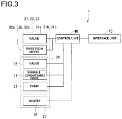
Atomic layer deposition apparatus
PatentActiveUS11634814B2
Innovation
- The apparatus features a vacuum chamber positioned between precursor sources of different temperatures, with short supply channels and lead-through connections that minimize distance to the deposition chamber, ensuring optimal thermal conditions and preventing cold spots by using a heated vacuum chamber and separate compartments for high and low temperature precursors.
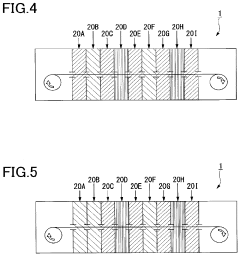
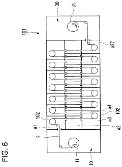
Atomic layer deposition apparatus and atomic layer deposition method
PatentPendingUS20220231259A1
Innovation
- The apparatus features multiple reaction chambers connected to separate supply pipes for precursors and purge gases, allowing for independent control of gas types and conditions, along with guide rollers and plasma electrodes, enabling precise adjustment of exposure conditions for each step during the ALD process.
Materials Compatibility and Durability Assessment
The compatibility of protective layers with photoelectrode materials represents a critical factor in determining the overall performance and longevity of photoelectrochemical cells (PECs). APALD (Atmospheric Pressure Atomic Layer Deposition) coatings must demonstrate excellent adhesion to various semiconductor surfaces while maintaining their protective properties in harsh electrochemical environments.
Material interface studies between APALD protective layers and common photoelectrode materials (Si, III-V semiconductors, metal oxides) reveal varying degrees of compatibility. Silicon-based photoelectrodes show exceptional compatibility with APALD-deposited TiO2 and Al2O3 layers, forming stable interfaces with minimal lattice mismatch. However, III-V semiconductors present more complex interfacial chemistry, often requiring intermediate buffer layers to prevent deleterious reactions during the deposition process.
Durability assessment protocols for APALD-protected photoelectrodes typically involve accelerated aging tests under simulated solar illumination in various electrolytes (pH 0-14). Recent studies demonstrate that optimized APALD TiO2 protective layers can maintain photoelectrode stability for over 1000 hours in strongly acidic or alkaline conditions, representing a significant improvement over previous protection strategies.
Chemical stability evaluations indicate that APALD-deposited metal oxides exhibit superior resistance to dissolution compared to conventionally deposited counterparts. This enhanced stability stems from the exceptional conformality and density of APALD films, which effectively block electrolyte penetration to the underlying photoelectrode. Particularly noteworthy is the stability of APALD-deposited TiO2 in both acidic and alkaline environments, making it a versatile protective material across various PEC applications.
Mechanical integrity assessments reveal that APALD protective layers maintain excellent adhesion even under the stress conditions induced by hydrogen or oxygen evolution reactions. Nanoindentation and scratch tests confirm that properly deposited APALD films withstand the mechanical stresses associated with gas evolution at the electrode surface without delamination or cracking.
Long-term stability studies tracking performance metrics (photocurrent density, onset potential, faradaic efficiency) demonstrate that APALD-protected photoelectrodes maintain >80% of their initial performance after extended operation periods, compared to rapid degradation of unprotected counterparts. This stability enhancement directly correlates with the thickness and quality of the APALD protective layer, with optimal protection typically achieved at 10-50 nm thickness depending on the specific photoelectrode material.
Temperature cycling experiments further validate the robustness of APALD protective layers, showing minimal degradation after repeated thermal cycling between ambient and elevated temperatures (up to 80°C). This thermal stability is particularly important for practical PEC applications where temperature fluctuations are common during operation.
Scalability and Cost Analysis for Commercial Implementation
The commercial implementation of APALD (Atomic Layer Deposition with Plasma Enhancement) technology for photoelectrode protection in photoelectrochemical cells faces significant scalability and cost challenges that must be addressed before widespread adoption can occur. Current APALD processes typically operate in batch mode with limited substrate dimensions, creating a bottleneck for large-scale production necessary for commercial photoelectrochemical applications.
Equipment costs represent a major barrier, with industrial-scale APALD systems ranging from $500,000 to $2 million, depending on chamber size and automation capabilities. These high capital expenditures necessitate substantial production volumes to achieve reasonable amortization periods, typically requiring 3-5 years for return on investment under optimal utilization scenarios.
Operational expenses further impact economic viability, with precursor chemicals constituting 15-25% of production costs. High-purity metal-organic compounds required for APALD processes command premium prices, while their limited shelf life adds inventory management complexities. Energy consumption during plasma generation and vacuum maintenance contributes an additional 10-15% to operational costs.
Process throughput remains a critical limitation, as APALD cycle times typically range from 0.5-2 seconds per monolayer. For protective coatings requiring 50-100 nm thickness (approximately 250-500 atomic layers), total deposition times can extend to several hours per batch, significantly constraining production capacity.
Recent innovations in spatial APALD and multi-wafer processing have demonstrated potential throughput improvements of 300-400%, though these approaches often require compromises in film uniformity and quality. Roll-to-roll APALD configurations show promise for flexible photoelectrodes, potentially reducing per-unit costs by 40-60% at scale, but face technical challenges in maintaining plasma stability across moving substrates.
Economic modeling suggests that APALD protective coatings add $2-5 per square foot to photoelectrode manufacturing costs at current technology readiness levels. This represents a significant percentage of total device costs, necessitating either performance improvements to justify the premium or process optimizations to reduce application expenses.
For commercial viability, research indicates that processing costs must decrease by approximately 65-75% while maintaining or improving coating quality. This cost reduction pathway will likely require simultaneous advances in precursor chemistry, equipment design, and process integration to achieve the necessary economic thresholds for market adoption.
Unlock deeper insights with Patsnap Eureka Quick Research — get a full tech report to explore trends and direct your research. Try now!
Generate Your Research Report Instantly with AI Agent
Supercharge your innovation with Patsnap Eureka AI Agent Platform!