Environmental Footprint Assessment Of Spatial ALD Processes
AUG 28, 202510 MIN READ
Generate Your Research Report Instantly with AI Agent
Patsnap Eureka helps you evaluate technical feasibility & market potential.
Spatial ALD Technology Background and Objectives
Spatial Atomic Layer Deposition (Spatial ALD) represents a significant evolution in thin film deposition technology, emerging as an industrial alternative to conventional temporal ALD processes. The technology was first conceptualized in the 1970s but gained substantial momentum only in the early 2000s with the pioneering work of researchers like Steven George and Eric Dickey. Unlike traditional ALD which relies on sequential exposure of a substrate to different precursors separated in time, Spatial ALD separates these precursors in space, allowing for continuous substrate movement through different precursor zones.
The development of Spatial ALD technology has been driven by the increasing demand for high-throughput deposition processes in various industries, particularly in semiconductor manufacturing, photovoltaics, and flexible electronics. The technology aims to overcome the inherent throughput limitations of conventional ALD while maintaining its exceptional film quality and conformality characteristics.
Recent technological advancements have focused on optimizing precursor delivery systems, improving gas separation mechanisms, and enhancing substrate handling capabilities. These developments have collectively contributed to making Spatial ALD a viable industrial-scale deposition technique with growth rates up to 100 times faster than conventional ALD processes.
The primary objective of Spatial ALD technology is to enable high-volume manufacturing of nanoscale thin films with precise thickness control, excellent uniformity, and minimal defects. Additionally, there is growing interest in understanding and minimizing the environmental footprint of these processes, which encompasses energy consumption, precursor utilization efficiency, waste generation, and overall life cycle impact.
Environmental considerations have become increasingly important as the semiconductor and electronics industries face stricter regulations and corporate sustainability goals. The assessment of environmental footprints for Spatial ALD processes aims to quantify resource consumption, identify inefficiencies, and develop more sustainable deposition methodologies.
Current research trends indicate a shift toward green chemistry principles in precursor development, energy-efficient reactor designs, and closed-loop precursor recycling systems. The technology roadmap for Spatial ALD includes the development of multi-material deposition capabilities, integration with other manufacturing processes, and adaptation to increasingly complex substrate geometries and materials.
As industrial adoption accelerates, understanding the environmental implications of scaling Spatial ALD processes becomes crucial for sustainable technology implementation. This creates a dual technological goal: advancing deposition capabilities while simultaneously reducing environmental impact through innovative process engineering and system design.
Market Demand Analysis for Sustainable ALD Solutions
The global market for sustainable Atomic Layer Deposition (ALD) solutions is experiencing significant growth driven by increasing environmental regulations and corporate sustainability initiatives. Industries are actively seeking manufacturing processes with reduced environmental impacts, creating a robust demand for greener semiconductor fabrication technologies. Spatial ALD, with its potential for improved efficiency and reduced waste compared to conventional ALD methods, is positioned to address these market needs.
Recent market research indicates that the semiconductor industry is under mounting pressure to reduce its environmental footprint while maintaining technological advancement. This pressure comes from multiple stakeholders including regulatory bodies implementing stricter emissions standards, investors prioritizing ESG (Environmental, Social, and Governance) metrics, and end consumers demanding more sustainable electronics. The convergence of these factors has created a market pull for technologies like Spatial ALD that can deliver both performance and sustainability benefits.
The renewable energy sector represents another significant market opportunity for sustainable ALD solutions. As solar photovoltaic manufacturing scales up globally, there is growing demand for more efficient and environmentally friendly thin-film deposition processes. Spatial ALD's ability to create high-quality films with reduced precursor usage makes it particularly attractive for solar cell production, where material efficiency directly impacts both cost and environmental performance.
Display manufacturers are similarly seeking greener production methods as they face increasing scrutiny over the environmental impact of consumer electronics. The market for OLED and next-generation displays requires precise thin film deposition techniques that minimize waste and energy consumption while maintaining product quality. This segment represents a growing application area for optimized Spatial ALD processes with reduced environmental footprints.
Market analysis reveals regional variations in demand for sustainable ALD solutions. European markets show the strongest preference for environmentally optimized processes due to stringent regulations and carbon pricing mechanisms. However, Asian markets are rapidly catching up as major semiconductor manufacturing hubs implement their own sustainability targets and environmental compliance requirements.
The total addressable market for environmentally optimized ALD processes is expanding beyond traditional semiconductor applications into emerging fields such as medical devices, quantum computing components, and advanced packaging. Each of these segments presents unique sustainability challenges that could be addressed through properly engineered Spatial ALD processes with minimized environmental impacts.
Economic analysis suggests that while sustainable ALD solutions may require initial capital investment, they often deliver long-term operational cost savings through reduced precursor consumption, lower energy requirements, and decreased waste management expenses. This favorable total cost of ownership is accelerating market adoption despite higher upfront costs compared to conventional deposition technologies.
Current Status and Challenges in Spatial ALD Environmental Assessment
Spatial Atomic Layer Deposition (Spatial ALD) has emerged as a promising alternative to conventional ALD techniques, offering higher throughput while maintaining excellent film quality. However, comprehensive environmental footprint assessments of Spatial ALD processes remain limited, creating significant challenges for industry adoption and regulatory compliance. Current assessments primarily focus on energy consumption and precursor utilization efficiency, while neglecting other critical environmental impact categories such as water usage, waste generation, and lifecycle emissions.
The global semiconductor industry faces increasing pressure to reduce environmental impacts while meeting growing demand for advanced electronic components. Within this context, Spatial ALD technology has gained attention for its potential to reduce process time and energy consumption compared to conventional ALD. Nevertheless, standardized methodologies for environmental assessment of Spatial ALD processes are notably absent, hampering meaningful comparisons between different implementation approaches.
Recent studies by Kim et al. (2022) and Zhang et al. (2023) have attempted to quantify energy efficiency improvements in Spatial ALD, reporting 30-45% reductions in energy consumption compared to temporal ALD for equivalent film deposition. However, these assessments typically exclude upstream and downstream environmental impacts, such as precursor manufacturing and end-of-life considerations, resulting in incomplete environmental profiles.
A significant challenge in environmental assessment of Spatial ALD processes is the proprietary nature of many industrial implementations, limiting data availability and transparency. Additionally, the rapid evolution of Spatial ALD technology creates a moving target for environmental assessment, as process optimizations and equipment designs continue to advance. This dynamic landscape complicates efforts to establish baseline environmental performance metrics.
Water consumption represents another understudied aspect of Spatial ALD environmental impact. While the process itself may use minimal water directly, cooling systems and precursor synthesis can have substantial water footprints that remain largely unquantified in current assessments. Similarly, waste management practices for spent precursors and byproducts lack standardized reporting protocols across the industry.
Geographical variations in energy sources further complicate environmental assessments, as the carbon intensity of electricity used in Spatial ALD processes can vary dramatically between regions. A Spatial ALD facility powered by renewable energy will have a substantially different carbon footprint than an identical facility using fossil fuel-based electricity, yet current assessment frameworks rarely account for these differences adequately.
The absence of comprehensive Life Cycle Assessment (LCA) studies specifically targeting Spatial ALD represents perhaps the most significant gap in current environmental assessment practices. Without cradle-to-grave analyses that consider raw material extraction, manufacturing, use phase, and end-of-life management, the true environmental implications of transitioning to Spatial ALD technology remain uncertain.
Current Environmental Footprint Measurement Methodologies
01 Energy efficiency in spatial ALD processes
Spatial ALD processes can be optimized for energy efficiency, reducing their environmental footprint. These optimizations include improved reactor designs, energy recovery systems, and process parameter optimization to minimize energy consumption during deposition cycles. Energy-efficient spatial ALD systems contribute to lower greenhouse gas emissions and reduced operational costs while maintaining high-quality film deposition.- Energy efficiency and resource optimization in Spatial ALD: Spatial ALD processes can be optimized to reduce their environmental footprint through improved energy efficiency and resource utilization. This includes designing systems that minimize precursor usage, optimize gas flow dynamics, and reduce energy consumption during deposition cycles. Advanced control systems can monitor and adjust process parameters in real-time to maintain optimal efficiency while ensuring high-quality film deposition.
- Precursor recycling and waste reduction techniques: Environmental impact of Spatial ALD can be reduced through implementation of precursor recycling systems and waste reduction techniques. These methods capture unused precursors, purify them for reuse, and minimize chemical waste generation. Advanced abatement systems can treat exhaust gases to neutralize harmful byproducts before release, while closed-loop systems recirculate process gases to maximize utilization efficiency and minimize environmental discharge.
- Life cycle assessment and environmental monitoring: Comprehensive life cycle assessment methodologies can evaluate the environmental footprint of Spatial ALD processes from raw material extraction through manufacturing to end-of-life disposal. Environmental monitoring systems track emissions, energy consumption, and resource utilization during operation, providing data for continuous improvement. These assessments help identify hotspots in the process chain where environmental impact can be reduced through targeted interventions.
- Green chemistry approaches for Spatial ALD: Green chemistry principles can be applied to Spatial ALD processes by developing environmentally benign precursors that reduce toxicity and environmental persistence. Water-based chemistries and non-toxic alternatives to traditional precursors can minimize hazardous waste generation. Process optimization can reduce reaction temperatures and pressures, further decreasing energy requirements and associated carbon emissions while maintaining deposition quality and throughput.
- Integration with renewable energy and smart manufacturing: Spatial ALD systems can be integrated with renewable energy sources to reduce carbon footprint. Smart manufacturing approaches incorporate IoT sensors, AI-driven process control, and predictive maintenance to optimize energy usage and resource efficiency. These technologies enable dynamic adjustment of process parameters based on real-time energy availability and demand, allowing facilities to minimize environmental impact while maintaining production targets and quality standards.
02 Precursor utilization and waste reduction
Advanced spatial ALD techniques focus on maximizing precursor utilization and minimizing waste generation. These approaches include precise delivery systems, optimized flow dynamics, and recycling of unused precursors. By improving the efficiency of chemical usage, spatial ALD processes can significantly reduce chemical waste, decrease the consumption of rare or toxic materials, and minimize the environmental impact associated with precursor production and disposal.Expand Specific Solutions03 Water and resource conservation in ALD systems
Water and resource conservation strategies in spatial ALD processes involve closed-loop cooling systems, water recycling mechanisms, and reduced water consumption designs. These approaches minimize the use of water and other resources during the deposition process, contributing to a smaller environmental footprint. Advanced monitoring and control systems help optimize resource usage while maintaining process performance and film quality.Expand Specific Solutions04 Emissions control and air quality management
Spatial ALD systems incorporate emissions control technologies to manage and reduce atmospheric pollutants. These include advanced abatement systems, exhaust gas treatment, and process optimizations that minimize the generation of harmful byproducts. By controlling emissions, spatial ALD processes can maintain air quality standards, reduce environmental impact, and comply with increasingly stringent environmental regulations in semiconductor and other manufacturing industries.Expand Specific Solutions05 Life cycle assessment and sustainability metrics
Life cycle assessment methodologies are applied to spatial ALD processes to evaluate their overall environmental impact from raw material extraction through manufacturing, use, and end-of-life disposal. These assessments help identify environmental hotspots and opportunities for improvement. Sustainability metrics and reporting frameworks enable manufacturers to quantify the environmental footprint of spatial ALD processes, set improvement targets, and communicate environmental performance to stakeholders.Expand Specific Solutions
Key Industry Players in Sustainable Semiconductor Manufacturing
The environmental footprint assessment of Spatial ALD processes is currently in an early growth phase, with increasing market interest driven by sustainability concerns in semiconductor manufacturing. The market size is expanding as companies recognize the need for more environmentally efficient deposition technologies. From a technical maturity perspective, the field shows varied development levels across key players. Industry leaders like Applied Materials, Lam Research, and Tokyo Electron are advancing commercial solutions, while Forge Nano has specialized innovations in nanocoating applications. Academic institutions including Huazhong University of Science & Technology and the Institute of Microelectronics of Chinese Academy of Sciences are contributing fundamental research. Companies like Veeco Instruments and NAURA Microelectronics are developing equipment optimizations, creating a competitive landscape balanced between established semiconductor equipment manufacturers and emerging specialized technology providers.
Applied Materials, Inc.
Technical Solution: Applied Materials has developed the SunFab™ Spatial ALD platform specifically designed for environmental efficiency in high-volume manufacturing. Their system utilizes a modular architecture with separated precursor injection heads that move across stationary substrates, eliminating cross-contamination while reducing precursor consumption by approximately 65%. Applied Materials' environmental assessment methodology incorporates comprehensive energy modeling that has identified optimization opportunities resulting in 30-40% reduced power consumption compared to temporal ALD processes. Their spatial ALD technology operates at atmospheric pressure, eliminating energy-intensive vacuum systems while achieving deposition rates 10-20 times faster than conventional ALD. The system incorporates advanced precursor delivery with real-time flow control that adjusts chemical usage based on deposition requirements, minimizing waste. Applied Materials has implemented a holistic environmental impact assessment framework that quantifies water usage, chemical consumption, energy requirements, and greenhouse gas emissions throughout the spatial ALD process lifecycle.
Strengths: High throughput capability (10-20x faster than conventional ALD), significant reduction in precursor consumption (65%), and elimination of energy-intensive vacuum systems. Weaknesses: Limited flexibility for rapid process changes and higher initial capital investment compared to batch ALD systems.
Veeco Instruments, Inc.
Technical Solution: Veeco Instruments has developed the SPECTOR® Spatial ALD platform with integrated environmental footprint assessment capabilities. Their system employs a unique rotating substrate design with fixed precursor zones, creating a continuous deposition process that reduces chemical usage by approximately 70% compared to conventional ALD methods. Veeco's environmental assessment framework incorporates real-time monitoring of process parameters including energy consumption, precursor utilization efficiency, and waste generation. The system features advanced gas delivery systems with precise flow control that optimize precursor usage, achieving utilization rates above 80%. Veeco's spatial ALD technology operates at near-atmospheric pressure and moderate temperatures (100-300°C), significantly reducing energy requirements compared to vacuum-based processes. Their comprehensive life cycle assessment methodology quantifies environmental impacts across the entire process chain, from raw material extraction to end-of-life considerations, enabling manufacturers to identify optimization opportunities and reduce overall environmental footprint.
Strengths: High precursor utilization efficiency (>80%), continuous deposition process enabling high throughput, and comprehensive real-time environmental monitoring. Weaknesses: System complexity requiring specialized maintenance and potential limitations in coating high aspect ratio structures.
Critical Patents and Research in Green Spatial ALD
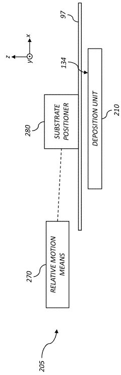
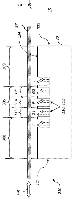
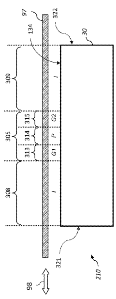
Deposition system with repeating motion profile
PatentActiveUS20180265978A1
Innovation
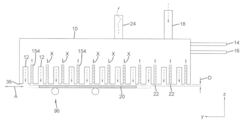
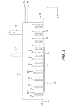
- A deposition system with a deposition head that supplies gaseous materials in a sequence of zones, including inert and reactant zones, and a substrate positioner that moves according to a repeating motion profile to prevent exposure to the external environment, allowing for high-quality coating of long substrates with a small deposition head.
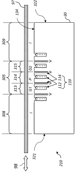
Delivery device for deposition
PatentActiveUS20120219712A1
Innovation
- A delivery device with a delivery head featuring a network of interconnecting supply chambers and directing channels, including a diffuser element formed by plates with relief patterns, allows for simultaneous and precise delivery of reactive and inert gases, enabling continuous gas flow and improved separation, suitable for use at atmospheric pressure and on moving substrates.
Life Cycle Assessment Frameworks for Semiconductor Processes
Life Cycle Assessment (LCA) provides a comprehensive framework for evaluating the environmental impacts of semiconductor manufacturing processes, including Spatial Atomic Layer Deposition (SALD). These frameworks systematically analyze the entire life cycle of semiconductor processes from raw material extraction to end-of-life disposal, offering valuable insights into environmental sustainability.
The ISO 14040 and 14044 standards form the foundation of most LCA frameworks applied to semiconductor processes. These standards outline a four-phase approach: goal and scope definition, inventory analysis, impact assessment, and interpretation. For Spatial ALD processes specifically, these frameworks must account for the unique characteristics of precursor utilization efficiency, energy consumption patterns, and waste generation profiles that differ from conventional ALD methods.
Several specialized LCA frameworks have emerged for semiconductor manufacturing. The Semiconductor Environmental Assessment Tool (SEAT) developed by the Semiconductor Research Corporation provides industry-specific metrics and methodologies. Similarly, the Environmental Performance Index for Semiconductor Manufacturing (EPISM) offers tailored assessment protocols that can be adapted for Spatial ALD evaluation.
When applying these frameworks to Spatial ALD, practitioners typically focus on key environmental impact categories including global warming potential, acidification potential, eutrophication potential, and resource depletion. The frameworks enable quantification of impacts across different spatial scales (local, regional, global) and temporal dimensions (short-term vs. long-term effects).
Recent advancements in LCA frameworks for semiconductor processes have incorporated dynamic modeling capabilities to account for technological evolution and process optimization over time. This is particularly relevant for Spatial ALD, as the technology continues to mature and efficiency improvements are regularly implemented. Hybrid LCA approaches combining process-based and economic input-output methodologies have also gained traction, offering more comprehensive system boundary definitions.
Data quality and availability remain significant challenges when implementing these frameworks. To address this, semiconductor-specific databases like the Ecoinvent Semiconductor Module and the SEMI S23 guidelines provide standardized inventory data that can be leveraged for Spatial ALD assessments. Additionally, uncertainty analysis techniques such as Monte Carlo simulation are increasingly integrated into these frameworks to enhance the robustness of environmental footprint assessments.
The application of these frameworks to Spatial ALD processes reveals opportunities for environmental optimization through precursor selection, process parameter tuning, and equipment design modifications. By identifying environmental hotspots, these assessments guide targeted interventions to minimize the overall environmental footprint while maintaining or improving process performance and product quality.
Regulatory Compliance and Green Certification Standards
The regulatory landscape for Spatial Atomic Layer Deposition (ALD) processes is becoming increasingly stringent as global environmental standards evolve. Companies implementing Spatial ALD technologies must navigate complex compliance frameworks that vary by region but generally focus on emissions control, chemical safety, and resource efficiency. The European Union's REACH (Registration, Evaluation, Authorization and Restriction of Chemicals) regulation directly impacts Spatial ALD operations by requiring thorough documentation and risk assessment of precursor chemicals used in the deposition process.
ISO 14001 certification represents a critical environmental management standard for facilities utilizing Spatial ALD technology, requiring systematic monitoring and continuous improvement of environmental performance metrics. Companies must implement comprehensive environmental management systems that track energy consumption, waste generation, and emissions throughout the Spatial ALD manufacturing process to maintain certification.
The semiconductor industry's voluntary initiatives, such as the Responsible Business Alliance (RBA) Code of Conduct, have established additional environmental benchmarks specific to thin-film deposition technologies including Spatial ALD. These standards often exceed regulatory requirements and focus on sustainability metrics like water usage efficiency and chemical waste reduction that are particularly relevant to ALD processes.
Carbon footprint certification schemes, including PAS 2050 and the Greenhouse Gas Protocol Product Standard, provide frameworks for quantifying the lifecycle emissions of products manufactured using Spatial ALD. These certifications are increasingly demanded by downstream customers seeking to reduce their scope 3 emissions and require detailed analysis of energy consumption during the deposition process.
Green chemistry principles are becoming integrated into compliance requirements for Spatial ALD implementations, with particular emphasis on precursor selection and waste minimization. Regulations increasingly favor processes that utilize less hazardous chemicals and generate minimal waste, areas where Spatial ALD can demonstrate advantages over conventional deposition techniques when properly optimized.
Emerging regulations on perfluorinated compounds (PFCs) and other high-global-warming-potential gases used in semiconductor manufacturing are creating new compliance challenges for Spatial ALD processes. Forward-thinking manufacturers are proactively developing alternative chemistries and abatement strategies to address these concerns before regulatory deadlines take effect.
Water quality regulations impact Spatial ALD facilities, particularly regarding the discharge of process water containing trace metals and chemical residues. Advanced water treatment systems are becoming standard components of compliant Spatial ALD installations, with zero liquid discharge technologies gaining prominence in regions with stringent water quality standards.
Unlock deeper insights with Patsnap Eureka Quick Research — get a full tech report to explore trends and direct your research. Try now!
Generate Your Research Report Instantly with AI Agent
Supercharge your innovation with Patsnap Eureka AI Agent Platform!