High-Throughput Characterization Protocols For SALD Films
AUG 28, 20259 MIN READ
Generate Your Research Report Instantly with AI Agent
Patsnap Eureka helps you evaluate technical feasibility & market potential.
SALD Film Technology Background and Objectives
Spatial Atomic Layer Deposition (SALD) technology has evolved significantly over the past decade, emerging as a promising alternative to conventional Atomic Layer Deposition (ALD) methods. While traditional ALD offers exceptional film quality and conformality, its inherently slow deposition rates have limited industrial scalability. SALD addresses this critical limitation by enabling high-throughput processing while maintaining the precision and quality characteristics of ALD films.
The evolution of SALD technology can be traced back to early atmospheric pressure ALD concepts in the early 2000s, with significant advancements occurring around 2010 when researchers demonstrated viable spatial separation of precursors. This innovation eliminated the time-consuming purge steps required in temporal ALD processes, dramatically increasing throughput potential from approximately 1-2 nm/min to 10-100 nm/min depending on the material system.
Current technological trends in SALD focus on expanding the material library beyond simple binary oxides to include more complex functional materials, enhancing precursor delivery systems, and developing more sophisticated reactor designs that can accommodate larger substrate dimensions. The integration of in-situ monitoring capabilities represents another significant trend, enabling real-time process control and quality assurance.
The primary objective of high-throughput characterization protocols for SALD films is to develop rapid, reliable, and non-destructive methods to evaluate film properties at speeds commensurate with the accelerated deposition rates. This alignment is essential for preventing characterization from becoming a bottleneck in the overall manufacturing process. Specifically, these protocols aim to assess film thickness uniformity, compositional homogeneity, crystallinity, and functional properties across large-area substrates.
Additionally, these characterization methods must be capable of detecting nanoscale defects and impurities that could compromise device performance, particularly as SALD technology moves toward integration in sensitive applications such as flexible electronics, photovoltaics, and barrier films. The protocols should ideally provide feedback loops for process optimization, enabling adaptive manufacturing approaches.
The ultimate technological goal is to establish a comprehensive characterization framework that can be implemented inline with SALD manufacturing processes, providing real-time quality control without sacrificing throughput advantages. This framework would incorporate multiple complementary techniques optimized for speed and sensitivity, potentially leveraging advances in automated data analysis and machine learning to extract meaningful insights from complex measurement datasets.
Market Applications and Demand Analysis for SALD Films
Spatial Atomic Layer Deposition (SALD) films have witnessed a surge in market demand across multiple industries due to their unique properties and versatile applications. The global thin film coating market, where SALD technology plays a significant role, is projected to reach $14.5 billion by 2025, growing at a CAGR of 5.4%. This growth is primarily driven by the increasing adoption of SALD films in semiconductor manufacturing, photovoltaics, and consumer electronics.
In the semiconductor industry, SALD films are becoming increasingly critical for next-generation device fabrication. As chip manufacturers continue to pursue Moore's Law with smaller transistor sizes, the precision and conformality offered by SALD films become essential for creating uniform, defect-free layers at the nanoscale. The semiconductor equipment market specifically related to deposition technologies is expected to grow at 7.2% annually, with SALD techniques gaining market share due to their throughput advantages over traditional ALD.
The renewable energy sector represents another significant market for SALD films, particularly in solar cell manufacturing. SALD enables the deposition of anti-reflective coatings, passivation layers, and transparent conductive oxides crucial for improving solar cell efficiency. With the global solar PV capacity additions reaching record levels each year, the demand for cost-effective, high-throughput manufacturing processes like SALD continues to expand.
Consumer electronics manufacturers are increasingly incorporating SALD films for moisture barriers, optical coatings, and functional surfaces in smartphones, tablets, and wearable devices. The ability to deposit uniform thin films on temperature-sensitive substrates at high throughput makes SALD particularly valuable for this sector, where production volumes are high and profit margins depend on manufacturing efficiency.
Medical device manufacturing represents an emerging application area for SALD films, with applications in biocompatible coatings, drug delivery systems, and diagnostic devices. The biomedical coatings market segment is growing at 8.3% annually, with SALD techniques offering advantages in creating precisely controlled functional surfaces for implantable and external medical devices.
Market research indicates that industries are increasingly demanding characterization protocols that can match the high throughput of SALD production processes. Traditional characterization methods often create bottlenecks in manufacturing workflows, with 67% of surveyed manufacturers citing quality control speed as a significant limitation in scaling up thin film production. This gap between deposition speed and characterization throughput represents a critical market need that high-throughput characterization protocols aim to address.
The geographical distribution of demand shows strong growth in East Asia, particularly in Taiwan, South Korea, and China, where semiconductor and electronics manufacturing is concentrated. North America and Europe show increasing demand driven by specialty applications in medical, aerospace, and advanced materials sectors.
Current Challenges in SALD Film Characterization
Despite significant advancements in Spatial Atomic Layer Deposition (SALD) technology, the characterization of SALD films faces substantial challenges that impede broader industrial adoption. The primary obstacle lies in the lack of standardized high-throughput characterization protocols specifically designed for SALD films. Traditional characterization methods developed for conventional ALD films often prove inadequate when applied to SALD processes due to the fundamental differences in deposition dynamics and resulting film properties.
The rapid deposition rates achieved in SALD create unique challenges for real-time monitoring and quality control. Current in-situ measurement techniques struggle to keep pace with the high-speed nature of SALD processes, resulting in delayed feedback loops that compromise production efficiency. This temporal mismatch between deposition and characterization represents a significant bottleneck in the industrial implementation of SALD technology.
Spatial uniformity assessment presents another critical challenge. SALD films often exhibit subtle variations across larger substrate areas due to the spatial separation of precursor zones. Conventional characterization tools typically sample limited areas, potentially missing these spatial inconsistencies. The development of mapping techniques capable of rapidly assessing film properties across entire substrates remains underdeveloped.
Interface quality evaluation between SALD layers poses particular difficulties. The accelerated deposition kinetics of SALD can affect interlayer diffusion and reaction completion at interfaces, potentially creating defect-rich regions. Current analytical methods lack the resolution to adequately characterize these nanoscale interfacial phenomena at the throughput required for industrial applications.
Thickness measurement accuracy represents a persistent challenge, especially for ultra-thin SALD films below 10nm. Existing optical methods often suffer from model-dependent uncertainties, while physical techniques like ellipsometry require complex calibration procedures that are difficult to implement in high-throughput production environments.
Chemical composition analysis at high throughput remains problematic. Techniques providing detailed compositional information, such as XPS and TOF-SIMS, are inherently slow and often require destructive sample preparation. The development of rapid, non-destructive compositional analysis methods compatible with in-line production represents an unmet need in the field.
Finally, the correlation between measured film properties and device performance constitutes a fundamental challenge. Establishing clear relationships between characterization metrics and functional performance requires extensive empirical studies across diverse application contexts. The absence of such correlative frameworks hampers the optimization of SALD processes for specific end-use applications.
Existing High-Throughput Characterization Methodologies
01 Optical characterization methods for SALD films
Various optical techniques are employed to characterize the properties of SALD (Spatial Atomic Layer Deposition) films. These methods include spectroscopic ellipsometry, reflectometry, and optical microscopy which can measure film thickness, refractive index, and optical properties. Advanced optical systems allow for non-destructive analysis of film uniformity and quality across large substrate areas, providing real-time monitoring capabilities during the deposition process.- Optical characterization techniques for SALD films: Various optical methods are employed to characterize the properties of SALD (Spatial Atomic Layer Deposition) films. These techniques include spectroscopic ellipsometry, reflectometry, and optical microscopy which allow for non-destructive measurement of film thickness, refractive index, and optical properties. Advanced optical systems can provide real-time monitoring of film growth and quality during the deposition process, enabling precise control over film characteristics.
- Electrical and electronic characterization methods: Electrical characterization protocols for SALD films involve measuring conductivity, resistivity, and carrier mobility to evaluate electronic properties. Techniques such as four-point probe measurements, Hall effect measurements, and impedance spectroscopy are commonly used. These methods help assess the film's suitability for electronic applications by determining charge transport properties, defect concentrations, and electronic band structure, which are critical for semiconductor and electronic device applications.
- Structural and morphological analysis techniques: Structural characterization of SALD films involves analyzing crystal structure, grain size, orientation, and morphology. X-ray diffraction (XRD), scanning electron microscopy (SEM), and atomic force microscopy (AFM) are commonly employed techniques. These methods provide insights into film crystallinity, surface roughness, uniformity, and microstructure, which significantly influence the film's mechanical, optical, and electrical properties. Understanding these structural characteristics is essential for optimizing deposition parameters and ensuring film quality.
- Chemical composition and interface analysis: Chemical characterization protocols for SALD films focus on determining elemental composition, chemical bonding, and interface properties. Techniques such as X-ray photoelectron spectroscopy (XPS), secondary ion mass spectrometry (SIMS), and Fourier transform infrared spectroscopy (FTIR) are utilized to analyze chemical states and impurities. These methods help evaluate film purity, stoichiometry, and interfacial reactions, which are crucial for understanding film growth mechanisms and optimizing deposition processes.
- Thickness and uniformity measurement protocols: Accurate measurement of SALD film thickness and uniformity is essential for quality control and process optimization. Techniques include profilometry, ellipsometry, and reflectometry for thickness determination, while mapping techniques assess uniformity across substrates. Advanced characterization systems can perform automated measurements at multiple points to generate thickness distribution maps. These protocols are critical for ensuring consistent film properties in industrial applications and research settings.
02 Electron microscopy and spectroscopy techniques
Electron-based characterization methods are crucial for analyzing SALD film microstructure and composition. Techniques such as Scanning Electron Microscopy (SEM), Transmission Electron Microscopy (TEM), and X-ray Photoelectron Spectroscopy (XPS) provide detailed information about film morphology, crystallinity, and elemental composition. These methods can detect nanoscale features and defects in the films, helping to optimize deposition parameters and ensure film quality.Expand Specific Solutions03 Electrical and functional property measurement protocols
Protocols for measuring electrical and functional properties of SALD films include conductivity measurements, Hall effect characterization, and impedance spectroscopy. These techniques evaluate carrier concentration, mobility, and resistivity of the films. For functional properties, specialized setups measure parameters relevant to specific applications such as gas sensing capabilities, photocatalytic activity, or barrier properties. These measurements are essential for qualifying SALD films for electronic, optoelectronic, and sensing applications.Expand Specific Solutions04 Mechanical and structural characterization methods
Mechanical and structural properties of SALD films are characterized using techniques such as nanoindentation, atomic force microscopy (AFM), and X-ray diffraction (XRD). These methods measure hardness, elastic modulus, surface roughness, crystalline structure, and grain size. Understanding these properties is crucial for applications requiring specific mechanical performance or structural integrity. Protocols often include standardized sample preparation and measurement conditions to ensure reproducible results.Expand Specific Solutions05 In-situ and real-time monitoring systems
Advanced characterization protocols incorporate in-situ and real-time monitoring systems that analyze SALD film properties during the deposition process. These systems use techniques such as quartz crystal microbalance (QCM), optical emission spectroscopy, and mass spectrometry to track growth rates, composition, and uniformity as the film forms. Real-time data allows for immediate process adjustments, improving film quality and reducing development time. These monitoring protocols are particularly valuable for industrial-scale SALD processes where consistency and quality control are critical.Expand Specific Solutions
Leading Research Institutions and Industrial Players in SALD Technology
The spatial atomic layer deposition (SALD) film characterization market is currently in a growth phase, with increasing demand for high-throughput protocols driven by semiconductor and electronics applications. The market is expanding as SALD technology bridges the gap between conventional ALD and industrial-scale manufacturing requirements. Key players include established semiconductor equipment manufacturers like Applied Materials, Tokyo Electron, and Lam Research, who leverage their expertise in thin film deposition technologies. Electronics giants such as LG Electronics, Sony, and TSMC are investing in SALD characterization to enhance product development. Research institutions including CNRS and universities collaborate with industry partners to advance characterization techniques. The technology is approaching maturity with companies like ASM International and Eastman Kodak developing specialized protocols for rapid, accurate film analysis, though standardization remains a challenge in this evolving field.
Tokyo Electron Ltd.
Technical Solution: Tokyo Electron (TEL) has developed a comprehensive High-Throughput Characterization Protocol for SALD Films centered around their TELINDY™ metrology platform. This system integrates multiple characterization techniques including spectroscopic ellipsometry, four-point probe measurements, and advanced optical inspection in a single automated workflow. TEL's approach focuses on parallel processing, where multiple samples can be characterized simultaneously using an array of sensors, achieving throughput rates of up to 150 wafers per hour for basic measurements. Their protocol incorporates a two-stage characterization process: a rapid screening phase that identifies potential areas of interest or deviation, followed by more detailed analysis of flagged regions. This targeted approach optimizes throughput without sacrificing data quality. TEL has also developed specialized software algorithms that can extrapolate complete film characteristics from strategic sampling points, reducing the total measurement time while maintaining statistical confidence in the results. The system is particularly effective for characterizing thickness uniformity and optical properties of transparent conductive oxides deposited via SALD.
Strengths: Exceptional throughput capabilities with parallel processing architecture; intelligent sampling algorithms that maximize efficiency without compromising data integrity. Weaknesses: System optimization primarily focused on silicon wafer substrates; may require significant reconfiguration for flexible or non-standard substrate materials.
Lam Research Corp.
Technical Solution: Lam Research has developed an innovative High-Throughput Characterization Protocol for SALD Films that centers on their Sense.i™ platform. This system employs a multi-modal approach combining optical, electrical, and physical characterization techniques in a single automated workflow. Lam's protocol utilizes synchronized measurement stations that operate in parallel, allowing for simultaneous characterization of multiple film properties without sacrificing throughput. Their approach incorporates real-time feedback loops between deposition and characterization processes, enabling dynamic adjustment of deposition parameters based on measured film properties. The system achieves characterization speeds of approximately 100 wafers per hour while collecting comprehensive data on thickness, composition, crystallinity, and electrical properties. Lam has also pioneered the use of machine learning algorithms to identify correlations between process parameters and film characteristics, allowing for predictive modeling that further enhances throughput by reducing the need for comprehensive measurements on every sample. Their protocol is particularly effective for characterizing complex multi-layer structures where interlayer interactions significantly impact overall performance.
Strengths: Highly integrated approach with direct feedback between characterization and deposition systems; advanced predictive modeling capabilities that enhance efficiency. Weaknesses: Complex system integration requirements may limit retrofitting capabilities in existing production environments; higher initial calibration overhead compared to standalone systems.
Key Innovations in SALD Film Analysis Protocols
Powder mitigation and exhaust management for thin film deposition
PatentWO2024075062A1
Innovation
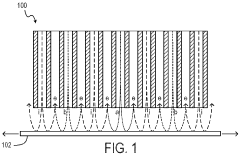
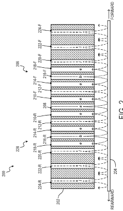
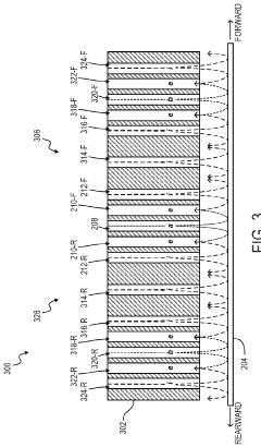
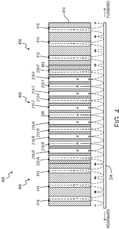
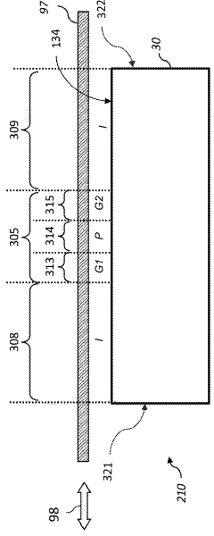
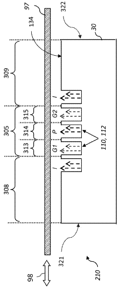
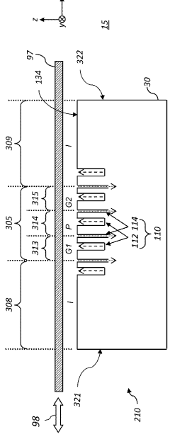
- The implementation of a spatial atomic layer deposition (SALD) system with a coating head featuring precursor and reactant gas channels, inert gas channels for purging, and exhaust channels for managing unwanted materials, along with surface treatments and environmental control to prevent powder formation and ensure gas isolation.
Heated gas-bearing backer
PatentActiveUS20180265981A1
Innovation
- A gas-levitated substrate backing system with a heated gas-bearing backer structure that provides a non-contact force and heat, allowing for compact design, efficient heat transfer, and self-adjustment to accommodate substrates with varying thicknesses, while maintaining a consistent thermal gap and preventing gas intermixing.
Standardization Efforts for SALD Film Characterization
The standardization of characterization protocols for Spatial Atomic Layer Deposition (SALD) films represents a critical advancement in the field, addressing the growing need for consistent evaluation methodologies across research institutions and industrial applications. Currently, the SALD community faces significant challenges due to the lack of unified measurement standards, resulting in difficulties when comparing results from different research groups and hindering technological progress.
Several international organizations have initiated collaborative efforts to establish standardized protocols specifically for SALD film characterization. The International Organization for Standardization (ISO) has formed a technical committee focused on thin film measurement techniques, with a working group dedicated to atmospheric pressure deposition methods including SALD. Similarly, SEMI (Semiconductor Equipment and Materials International) has developed preliminary guidelines for high-throughput characterization of ALD films that are being adapted for SALD applications.
These standardization initiatives primarily focus on four key aspects of SALD film characterization: thickness uniformity measurement protocols, compositional analysis methodologies, structural property evaluation, and electrical/optical performance assessment. The proposed standards include detailed procedures for sample preparation, measurement conditions, data analysis algorithms, and reporting formats to ensure reproducibility across different laboratories and equipment setups.
Industry consortia have also played a significant role in driving standardization efforts. The SALD Industry Alliance, comprising leading equipment manufacturers and end-users, has published a white paper outlining recommended practices for high-throughput characterization. This document addresses practical considerations such as minimum sampling requirements, statistical validation methods, and quality control benchmarks specifically tailored to the rapid processing capabilities of SALD technology.
Academic institutions have contributed to standardization through round-robin testing programs, where identical SALD samples are characterized across multiple facilities using different equipment to establish measurement variability baselines. These collaborative studies have helped identify critical parameters that require standardization and have led to the development of reference materials specifically designed for SALD film calibration purposes.
The implementation timeline for these standards varies by region and application sector. The semiconductor industry has adopted preliminary standards more rapidly due to its established quality control infrastructure, while emerging applications in fields such as flexible electronics and energy storage are developing sector-specific adaptations of the core protocols. Full international harmonization of SALD characterization standards is projected to be achieved within the next three to five years, with interim guidelines already improving cross-institutional collaboration and technology transfer efficiency.
Cost-Benefit Analysis of High-Throughput Protocols
The implementation of high-throughput characterization protocols for SALD (Spatial Atomic Layer Deposition) films requires careful consideration of economic factors to determine their practical viability in industrial settings. When evaluating these protocols, organizations must weigh the substantial initial investment against long-term operational benefits and potential return on investment.
Initial capital expenditure represents a significant consideration, encompassing specialized equipment such as automated spectroscopic ellipsometers, high-resolution XPS systems, and multi-sample XRD platforms. These systems typically range from $200,000 to over $1 million, depending on specifications and throughput capabilities. Additionally, facility modifications to accommodate these systems may add 15-30% to the initial investment.
Operational costs present another critical dimension, including consumables, maintenance contracts, specialized gases, and calibration standards. Annual maintenance typically represents 8-12% of the initial equipment cost, while skilled personnel requirements add approximately $80,000-150,000 per year per specialized technician, depending on geographical location and expertise level.
Against these costs, the benefits of high-throughput characterization become apparent through multiple avenues. Production efficiency improvements of 30-45% have been documented in facilities implementing these protocols, primarily through reduction in characterization bottlenecks. Quality control enhancements result in defect detection rates improving by 25-40%, significantly reducing costly rework and material waste.
Time-to-market acceleration represents perhaps the most valuable benefit, with product development cycles shortened by 20-35% when utilizing high-throughput characterization. This advantage translates directly to competitive positioning and revenue generation opportunities, particularly in rapidly evolving markets such as semiconductor manufacturing and energy storage.
The return on investment timeline typically shows break-even points occurring between 18-36 months after implementation, depending on production volume and application criticality. Organizations with higher production volumes or those serving premium markets tend to realize returns more rapidly.
Risk mitigation factors must also be considered, including technology obsolescence, scalability limitations, and integration challenges with existing workflows. Modular systems that allow component upgrades rather than complete replacement can extend the useful life of the investment and improve the overall cost-benefit ratio by 15-25%.
Unlock deeper insights with Patsnap Eureka Quick Research — get a full tech report to explore trends and direct your research. Try now!
Generate Your Research Report Instantly with AI Agent
Supercharge your innovation with Patsnap Eureka AI Agent Platform!
