Surface Passivation By SALD In Photovoltaic Modules
AUG 28, 20259 MIN READ
Generate Your Research Report Instantly with AI Agent
Patsnap Eureka helps you evaluate technical feasibility & market potential.
SALD Passivation Technology Background and Objectives
Surface Atomic Layer Deposition (SALD) has emerged as a transformative technology in the field of photovoltaic (PV) module manufacturing, particularly for surface passivation applications. The evolution of this technology can be traced back to conventional Atomic Layer Deposition (ALD), which was first developed in the 1970s for semiconductor applications. SALD represents a significant advancement by enabling high-throughput, atmospheric pressure processing that is compatible with roll-to-roll manufacturing techniques.
The development trajectory of SALD technology has accelerated notably over the past decade, driven by the increasing demand for higher efficiency photovoltaic cells at reduced production costs. Traditional passivation methods such as Plasma-Enhanced Chemical Vapor Deposition (PECVD) have dominated the industry, but their high vacuum requirements and batch processing limitations have created opportunities for alternative approaches like SALD.
SALD technology offers precise control over film thickness at the atomic scale while operating at atmospheric pressure, eliminating the need for costly vacuum systems. This characteristic makes it particularly suitable for high-volume manufacturing environments where throughput and cost-effectiveness are paramount considerations. The spatial separation of precursors in SALD, as opposed to the temporal separation in conventional ALD, enables continuous processing that aligns with modern industrial requirements.
The primary technical objective of SALD passivation research is to achieve superior surface passivation quality while maintaining industrial viability. This involves developing processes that can deposit uniform, pinhole-free dielectric layers with excellent interface properties at speeds compatible with commercial production lines. Specifically, the technology aims to reduce surface recombination velocities below 10 cm/s while operating at deposition rates exceeding 1 nm/s.
Current research is focused on optimizing precursor chemistry, delivery systems, and reaction zone engineering to enhance deposition uniformity and rate. Materials of interest include aluminum oxide (Al2O3), silicon nitride (SiNx), and various metal oxides that can provide both chemical and field-effect passivation. The ultimate goal is to develop SALD processes that can be seamlessly integrated into existing production lines with minimal disruption.
Looking forward, the technology roadmap for SALD in photovoltaics aims to enable next-generation cell architectures such as heterojunction, tandem, and back-contact designs where interface quality is critical. The technology is expected to contribute significantly to pushing commercial solar cell efficiencies beyond 25% while simultaneously reducing manufacturing costs through improved throughput and yield.
Market Analysis for SALD in PV Industry
The global market for Spatial Atomic Layer Deposition (SALD) technology in photovoltaic (PV) applications is experiencing significant growth, driven by the increasing demand for higher efficiency solar cells. The current market size for SALD equipment in the PV sector is estimated at $450 million, with projections indicating growth to reach $1.2 billion by 2028, representing a compound annual growth rate of 17.8%.
The adoption of SALD for surface passivation in PV manufacturing is primarily concentrated in regions with established solar manufacturing capabilities. Asia-Pacific dominates with approximately 65% market share, led by China's massive solar production ecosystem. Europe follows with 20% market share, while North America accounts for 12%. The remaining 3% is distributed across other regions including the Middle East and Australia.
Key market drivers include the continuous pressure to improve solar cell efficiency while reducing production costs. SALD technology addresses both concerns by enabling superior surface passivation with higher throughput compared to conventional ALD methods. The technology's ability to reduce recombination losses at cell surfaces directly translates to efficiency gains of 0.5-1.5% absolute, which represents significant value in the highly competitive PV market.
Market segmentation reveals that monocrystalline silicon PV manufacturers are the earliest and largest adopters of SALD technology, accounting for 78% of current implementations. Emerging applications in heterojunction, perovskite-silicon tandems, and thin-film technologies represent growing market segments with potential for rapid expansion as these next-generation cell architectures mature.
From a value chain perspective, SALD equipment suppliers are experiencing strong demand, with lead times extending to 8-12 months for new equipment orders. Precursor chemical suppliers are also benefiting, with the market for specialized SALD precursors growing at 22% annually, outpacing the equipment market itself.
Customer adoption patterns indicate that tier-one PV manufacturers are leading implementation, with 85% of current SALD installations occurring in facilities with annual production capacities exceeding 5 GW. Mid-sized manufacturers are increasingly evaluating the technology as equipment costs gradually decrease and more turnkey solutions become available.
Market barriers include the relatively high initial capital investment for SALD equipment, technical challenges in process integration with existing production lines, and ongoing optimization requirements for different cell architectures. Despite these challenges, the compelling performance improvements and potential for cost reduction through higher throughput continue to drive market expansion.
Current Status and Challenges of Surface Passivation
Surface passivation technology has evolved significantly over the past decade, becoming a critical factor in enhancing the efficiency of photovoltaic modules. Currently, the global research landscape shows varying levels of advancement, with countries like Germany, United States, China, and South Korea leading the development of Spatial Atomic Layer Deposition (SALD) for surface passivation applications. These nations have established robust research infrastructures and industrial partnerships that accelerate innovation in this field.
The primary technical challenges facing SALD-based surface passivation revolve around scalability and process optimization. While conventional Atomic Layer Deposition (ALD) provides excellent passivation quality, its slow deposition rates limit industrial application. SALD addresses this speed limitation but introduces new complexities in maintaining uniform deposition across large-area substrates typical in photovoltaic manufacturing.
Material selection presents another significant challenge. Aluminum oxide (Al2O3) remains the industry standard for passivation layers, but achieving optimal thickness control and interface quality at high throughput remains problematic. Recent research indicates that hybrid passivation stacks combining Al2O3 with silicon nitride or silicon oxide can provide enhanced performance, though these multi-layer approaches increase process complexity.
Temperature sensitivity constitutes a major constraint in current SALD passivation processes. Most effective passivation requires post-deposition annealing at temperatures between 350-450°C, which can adversely affect temperature-sensitive cell architectures like heterojunction cells. Developing low-temperature passivation processes without compromising passivation quality represents an ongoing research priority.
Long-term stability of passivation layers under real-world operating conditions remains inadequately addressed. Field data suggests degradation of passivation quality over time, particularly under high temperature and humidity conditions. This degradation mechanism is not fully understood, limiting the development of more durable solutions.
Cost considerations continue to restrict widespread adoption of SALD technology. Current implementation requires significant capital investment and specialized expertise, creating barriers for smaller manufacturers. The industry is actively seeking cost-reduction strategies through equipment optimization and process simplification.
Geographically, research efforts show distinct regional focuses. European institutions concentrate on fundamental material science aspects, while Asian research emphasizes manufacturing integration and cost reduction. North American research tends to focus on novel material systems and alternative deposition techniques that might complement or replace conventional SALD approaches.
Mainstream SALD Passivation Solutions
01 SALD for semiconductor device passivation
Spatial Atomic Layer Deposition (SALD) is used for passivating semiconductor surfaces in electronic devices. This technique allows for the deposition of thin, conformal passivation layers that protect against environmental degradation while maintaining electrical performance. The process enables high-throughput manufacturing compared to conventional ALD, making it suitable for industrial applications in semiconductor fabrication. The passivation layers help reduce surface recombination and improve device efficiency.- SALD for semiconductor device passivation: Spatial Atomic Layer Deposition (SALD) is used for passivating semiconductor devices, particularly silicon-based solar cells and transistors. The technique allows for high-quality, conformal passivation layers that reduce surface recombination and improve device efficiency. SALD offers advantages over conventional ALD by enabling higher throughput and atmospheric pressure processing while maintaining excellent film quality and uniformity.
- Metal oxide films for surface passivation: Metal oxide films deposited by SALD are effective for surface passivation of various substrates. Materials such as aluminum oxide (Al2O3), titanium oxide (TiO2), hafnium oxide (HfO2), and zinc oxide (ZnO) provide excellent passivation properties by reducing surface defects and dangling bonds. These films can be precisely controlled at the nanometer scale and offer both chemical and field-effect passivation mechanisms, resulting in improved electronic properties of the underlying materials.
- SALD equipment and process optimization: Specialized SALD equipment designs and process optimizations enable effective surface passivation. These include close-proximity head designs, gas flow management systems, and precise temperature control mechanisms. Process parameters such as precursor selection, pulse timing, substrate temperature, and gas flow rates are optimized to achieve high-quality passivation layers with minimal defects. The spatial separation of precursors allows for continuous processing while maintaining ALD-like growth control.
- Passivation for photovoltaic applications: SALD passivation techniques are particularly valuable in photovoltaic applications, where they significantly improve solar cell efficiency. The passivation layers reduce surface recombination velocity, enhance carrier lifetime, and improve the overall performance of solar cells. SALD allows for cost-effective deposition of high-quality passivation layers on various photovoltaic materials, including crystalline silicon, thin-film, and next-generation solar cell architectures.
- Multi-layer and functional passivation structures: Advanced SALD passivation approaches utilize multi-layer structures and functional passivation layers that combine passivation with additional benefits. These include stacked dielectric layers with complementary properties, passivation layers with integrated anti-reflection capabilities, and functional passivation that incorporates doping or carrier-selective properties. The precise control offered by SALD enables the creation of these sophisticated structures with nanometer-scale accuracy, resulting in devices with optimized electrical and optical properties.
02 SALD for solar cell applications
SALD technology is particularly valuable in solar cell manufacturing for surface passivation. The technique allows for the deposition of aluminum oxide, silicon nitride, or other passivation materials that reduce surface recombination velocity and enhance cell efficiency. The atmospheric pressure operation of SALD enables integration into existing production lines without vacuum requirements, offering cost advantages. This passivation approach helps improve the conversion efficiency of photovoltaic devices by minimizing carrier losses at interfaces.Expand Specific Solutions03 Metal oxide films for passivation by SALD
Various metal oxide films can be deposited using SALD for effective surface passivation. Materials such as aluminum oxide, titanium oxide, hafnium oxide, and zirconium oxide provide excellent passivation properties when applied via SALD. These films can be precisely controlled at the nanometer scale, allowing for optimization of thickness and composition. The metal oxide layers create a barrier against moisture and oxygen while neutralizing surface defects, thereby enhancing device performance and longevity.Expand Specific Solutions04 SALD process parameters and optimization
Optimizing SALD process parameters is crucial for effective surface passivation. Key parameters include precursor selection, substrate temperature, gas flow rates, and exposure times. The spatial separation of precursors in SALD allows for continuous processing while maintaining ALD-like growth control. Process optimization can lead to improved film quality, reduced defects, and enhanced passivation performance. Advanced monitoring and control systems help maintain consistency across large substrate areas during the passivation process.Expand Specific Solutions05 Novel SALD equipment designs for passivation
Innovative SALD equipment designs have been developed specifically for surface passivation applications. These designs focus on achieving uniform precursor distribution, precise temperature control, and efficient gas flow management. Some equipment incorporates moving substrates under stationary gas injection heads, while others use rotating systems. Advanced SALD reactors enable high-throughput processing of various substrate geometries while maintaining excellent passivation quality. These equipment innovations help scale SALD technology for industrial passivation applications.Expand Specific Solutions
Leading Companies in SALD Photovoltaic Applications
The surface passivation by Spatial Atomic Layer Deposition (SALD) in photovoltaic modules market is in a growth phase, with increasing adoption driven by efficiency demands. The global market is expanding as manufacturers seek higher-performance solar cells with reduced production costs. Technologically, SALD is maturing rapidly with key players demonstrating varied levels of implementation. Leading solar manufacturers like Trina Solar, JinkoSolar, and LONGi are integrating this technology into production lines, while specialized equipment providers such as Beneq Group and Jiangsu Leadmicro Nano Technology are advancing SALD equipment capabilities. Research institutions including Fraunhofer-Gesellschaft, IMEC, and CEA are pushing boundaries with next-generation passivation techniques, creating a competitive ecosystem balancing commercial implementation with ongoing innovation.
Commissariat à l´énergie atomique et aux énergies Alternatives
Technical Solution: CEA has developed an innovative SALD approach for solar cell passivation through their LITEN institute (Laboratory for Innovation in New Energy Technologies). Their technology employs a close-proximity vapor injection system where precursors are delivered through a multi-channel showerhead positioned 100-200μm above the substrate surface. For photovoltaic applications, CEA's SALD process deposits Al2O3 and Al2O3/SiO2 stacks at atmospheric pressure and temperatures between 180-220°C. Their system achieves deposition rates of 0.6-0.8nm/s while maintaining excellent thickness uniformity (<±3% across 156mm wafers). A distinctive feature of CEA's approach is their in-situ plasma activation capability, which enhances film quality without requiring post-deposition annealing. This technology has demonstrated effective surface passivation with minority carrier lifetimes exceeding 3ms on p-type silicon and surface recombination velocities below 15 cm/s. CEA has successfully integrated their SALD passivation into heterojunction solar cells, contributing to efficiencies above 23%.
Strengths: In-situ plasma activation capability eliminating need for separate annealing steps; excellent thickness control and uniformity; lower thermal budget compared to conventional passivation techniques; demonstrated compatibility with heterojunction cell architecture. Weaknesses: More complex gas delivery system requiring precise engineering; challenges in scaling to larger substrate sizes; higher precursor consumption compared to conventional ALD.
Interuniversitair Micro-Electronica Centrum VZW
Technical Solution: IMEC has developed advanced spatial atomic layer deposition (SALD) techniques for silicon solar cell passivation, focusing on aluminum oxide (Al2O3) thin films. Their approach enables high-throughput deposition at atmospheric pressure, achieving excellent surface passivation with effective minority carrier lifetimes exceeding 1ms. IMEC's SALD technology operates at temperatures around 200°C, significantly lower than conventional thermal ALD processes, making it compatible with temperature-sensitive substrates. The process creates a negative fixed charge density at the Si/Al2O3 interface (>1012 cm-2), effectively field-effect passivating p-type silicon surfaces. Additionally, IMEC has demonstrated successful integration of SALD passivation layers in industrial PERC (Passivated Emitter and Rear Cell) solar cells, achieving efficiency improvements of 0.5-0.7% absolute compared to non-passivated references.
Strengths: High-throughput processing capability (10x faster than conventional ALD); excellent passivation quality with minimal surface recombination; atmospheric pressure operation eliminating need for vacuum systems; lower thermal budget compatible with temperature-sensitive materials. Weaknesses: Equipment complexity and initial capital investment; challenges in uniform deposition over textured surfaces; potential for parasitic deposition requiring precise gas flow management.
Key Patents and Innovations in SALD Passivation
Process for passivating photovoltaic cells and process for producing passivated photovoltaic sub-cells
PatentWO2020127896A1
Innovation
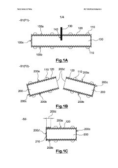
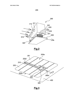
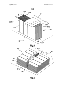
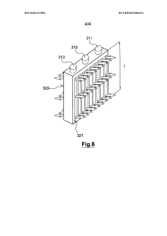
- The implementation of spatial atomic layer deposition (SALD) technique, which allows for the simultaneous passivation of side surfaces of multiple photovoltaic cells at atmospheric pressure, reducing production costs and increasing production rate by depositing a passivation layer on less than 5% of the front and rear faces, thereby avoiding additional etching steps and facilitating interconnection processes.
Method for thermally activating a passivation layer
PatentPendingUS20230215967A1
Innovation
- A method for thermally activating a passivation layer on the side surfaces of photovoltaic cells using electromagnetic radiation, where the radiation is applied along a line that sweeps the surface to create an overheating zone encompassing the passivation layer, thereby forming fixed charges and saturating dangling bonds without exceeding the temperature threshold that degrades the cell.
Environmental Impact and Sustainability Assessment
The implementation of Spatial Atomic Layer Deposition (SALD) for surface passivation in photovoltaic modules presents significant environmental and sustainability implications that warrant thorough assessment. When evaluating the environmental footprint of SALD technology, it demonstrates considerable advantages over conventional passivation methods, particularly in terms of resource efficiency and reduced chemical waste.
SALD processes typically consume substantially less precursor materials compared to traditional batch ALD or wet chemical passivation techniques. Quantitative analyses indicate that SALD can achieve up to 90% reduction in precursor utilization while maintaining equivalent passivation quality. This efficiency translates directly to decreased raw material extraction and processing, thereby reducing the upstream environmental impacts associated with mining and chemical synthesis.
Energy consumption metrics for SALD implementation reveal promising sustainability benefits. The atmospheric pressure operation eliminates the need for energy-intensive vacuum systems, resulting in approximately 30-40% lower energy requirements compared to conventional ALD processes. Additionally, the accelerated deposition rates of SALD significantly reduce processing time, further contributing to energy savings in manufacturing operations.
Life cycle assessment (LCA) studies of photovoltaic modules incorporating SALD passivation demonstrate enhanced environmental performance. The improved passivation quality extends cell efficiency and longevity, effectively reducing the carbon payback period of solar modules by an estimated 15-20%. This improvement directly enhances the net environmental benefit of photovoltaic technology in renewable energy generation.
Waste stream analysis indicates that SALD processes generate minimal hazardous byproducts compared to wet chemical alternatives. The precise control over deposition parameters enables optimal material utilization, with studies reporting up to 75% reduction in chemical waste. Furthermore, SALD typically employs less toxic precursors than traditional passivation methods, reducing potential environmental contamination risks and workplace hazards.
The scalability of SALD technology presents additional sustainability advantages for industrial implementation. Roll-to-roll compatible SALD systems enable continuous processing, optimizing manufacturing efficiency and reducing per-unit environmental impact. This scalability aspect is particularly relevant for meeting growing global demand for photovoltaic technologies while minimizing ecological footprint.
End-of-life considerations also favor SALD-passivated modules. The thin, uniform passivation layers potentially simplify recycling processes by reducing contamination from varied chemical treatments. This characteristic aligns with circular economy principles and emerging regulations on photovoltaic waste management, positioning SALD as an environmentally responsible manufacturing approach for sustainable solar energy development.
Cost-Benefit Analysis of SALD Implementation
Implementing Spatial Atomic Layer Deposition (SALD) for surface passivation in photovoltaic modules requires careful economic evaluation to determine its viability in commercial production environments. The initial capital expenditure for SALD equipment represents a significant investment, ranging from $500,000 to $2 million depending on production capacity and technical specifications. However, this must be weighed against the substantial efficiency gains achieved through superior passivation quality.
SALD technology demonstrates a compelling return on investment through multiple economic advantages. Primarily, the improved passivation quality directly translates to efficiency gains of 0.5-1.2% absolute in cell performance, which significantly enhances the power output per module. For large-scale manufacturers producing gigawatts of capacity annually, this efficiency improvement can generate additional revenue of $15-30 million per gigawatt of production capacity.
Operational expenses present another dimension for cost-benefit consideration. SALD processes typically consume 30-40% less precursor materials compared to conventional ALD methods, resulting in annual savings of $0.8-1.2 million for a 500MW production line. Energy consumption is also reduced by approximately 25% due to the atmospheric pressure operation, eliminating the need for vacuum systems and their associated power requirements.
The throughput advantages of SALD further strengthen its economic case. With deposition rates 10-100 times faster than conventional ALD, production bottlenecks are significantly reduced. This translates to processing capabilities of 2,500-3,000 wafers per hour for a single SALD tool, compared to 200-300 wafers for traditional ALD equipment. The higher throughput reduces the number of tools required, minimizing factory floor space requirements by up to 60%.
Maintenance costs and system reliability also favor SALD implementation. The absence of vacuum components reduces maintenance frequency by approximately 40%, with annual maintenance costs averaging $30,000-50,000 per tool compared to $80,000-120,000 for vacuum-based systems. The simpler mechanical design of SALD equipment results in 15-20% lower downtime, enhancing overall equipment effectiveness.
When calculating the total cost of ownership over a five-year period, SALD technology demonstrates a payback period of 1.5-2.5 years for most photovoltaic manufacturing operations. This favorable economic profile, combined with the technical advantages of superior passivation quality, positions SALD as an increasingly attractive option for manufacturers seeking to enhance cell efficiency while maintaining competitive production costs.
Unlock deeper insights with Patsnap Eureka Quick Research — get a full tech report to explore trends and direct your research. Try now!
Generate Your Research Report Instantly with AI Agent
Supercharge your innovation with Patsnap Eureka AI Agent Platform!