

Case Study: SALD Implementation In Printed Electronics Line
AUG 28, 20259 MIN READ
Generate Your Research Report Instantly with AI Agent
PatSnap Eureka helps you evaluate technical feasibility & market potential.
SALD Technology Background and Implementation Goals
Spatial Atomic Layer Deposition (SALD) represents a significant evolution in thin-film deposition technology, emerging as a response to the limitations of conventional Atomic Layer Deposition (ALD) processes. Traditional ALD, while offering exceptional film quality and conformality, has been constrained by low throughput and vacuum requirements, making it challenging to integrate into high-volume manufacturing environments, particularly for printed electronics applications.
SALD technology originated in the early 2000s, with pioneering work by researchers seeking to overcome these limitations. The fundamental innovation of SALD lies in its spatial separation of precursor gases, as opposed to the temporal separation used in conventional ALD. This breakthrough enables continuous deposition processes at atmospheric pressure, dramatically increasing throughput while maintaining the precision and quality characteristics of ALD.
The evolution of SALD has been marked by progressive improvements in precursor delivery systems, gas flow management, and substrate handling mechanisms. Early prototypes demonstrated proof-of-concept but faced challenges in uniformity and scalability. Recent advancements have focused on optimizing gas flow dynamics, precursor chemistry, and mechanical design to achieve industrial-scale implementation capabilities.
In the context of printed electronics, SALD offers unique advantages that align with industry requirements for high-throughput, cost-effective manufacturing of flexible and large-area electronic devices. The technology enables the deposition of high-quality metal oxide semiconductors, dielectrics, and barrier layers essential for various electronic components, including thin-film transistors, sensors, and photovoltaic cells.
The primary implementation goals for SALD in printed electronics production lines center on several critical objectives. First, seamless integration with existing roll-to-roll (R2R) or sheet-to-sheet manufacturing processes is essential to maintain production efficiency. Second, achieving consistent film quality across large substrate areas with nanometer-level thickness control represents a fundamental technical requirement.
Additionally, implementation aims include optimizing process parameters to ensure compatibility with temperature-sensitive flexible substrates, which typically cannot withstand the elevated temperatures used in conventional semiconductor manufacturing. Speed enhancement is another crucial goal, with target deposition rates significantly higher than traditional ALD while maintaining film quality and uniformity.
Cost-effectiveness represents a paramount implementation objective, as the economic viability of SALD technology depends on demonstrating clear advantages in terms of capital expenditure, operational costs, and overall production economics compared to alternative deposition methods. Finally, environmental considerations drive goals related to precursor utilization efficiency, waste reduction, and overall process sustainability.
Market Analysis for SALD in Printed Electronics
The global market for Spatial Atomic Layer Deposition (SALD) in printed electronics is experiencing robust growth, driven by increasing demand for flexible, lightweight, and cost-effective electronic components. Current market valuations indicate that the printed electronics sector is expanding at a compound annual growth rate of approximately 13.6%, with the SALD technology segment showing particularly strong momentum due to its unique advantages in thin-film deposition processes.
The demand for SALD technology is primarily fueled by several key application areas within printed electronics. Consumer electronics represents the largest market segment, where SALD enables the production of next-generation displays, touch panels, and flexible circuits. The automotive industry follows closely, incorporating printed electronics for dashboard displays, sensors, and lighting systems that benefit from SALD's precision coating capabilities.
Healthcare applications constitute another significant market segment, with medical devices increasingly utilizing printed electronics for wearable health monitors, smart bandages, and diagnostic equipment. The energy sector also shows substantial growth potential, particularly in the manufacturing of photovoltaic cells and energy storage devices where SALD offers superior performance characteristics compared to traditional deposition methods.
Geographically, Asia-Pacific dominates the market landscape, accounting for over 45% of global SALD implementation in printed electronics. This regional leadership is attributed to the concentration of electronics manufacturing facilities in countries like South Korea, Japan, China, and Taiwan. North America and Europe represent secondary but rapidly growing markets, driven by research institutions and specialized electronics manufacturers focusing on high-value applications.
Market analysis reveals several key trends shaping the SALD landscape in printed electronics. First, there is increasing integration of SALD processes into roll-to-roll manufacturing systems, enabling higher throughput and reduced production costs. Second, material innovations are expanding the range of functional thin films that can be deposited using SALD, opening new application possibilities. Third, miniaturization trends in electronics are creating demand for more precise deposition technologies, where SALD excels due to its nanometer-scale thickness control.
Customer requirements are evolving toward higher performance specifications, with particular emphasis on uniformity of coating, process reliability, and integration capabilities with existing production lines. The market shows strong preference for SALD systems that offer versatility across different substrate materials and can accommodate varying production volumes, from small-batch specialty products to high-volume consumer electronics.
Current SALD Implementation Challenges
Despite the promising potential of Spatial Atomic Layer Deposition (SALD) in printed electronics manufacturing, several significant implementation challenges currently impede its widespread industrial adoption. The primary technical obstacle remains the precise control of gas flow dynamics within the deposition chamber. Unlike traditional ALD which operates in vacuum conditions, SALD functions at atmospheric pressure, creating complex gas flow patterns that can lead to precursor mixing and subsequent CVD-like reactions, compromising the self-limiting nature of ALD processes.
Equipment scaling presents another formidable challenge. Current SALD systems demonstrate excellent performance at laboratory scale but encounter significant engineering difficulties when scaled to production-level throughput requirements. The need to maintain uniform gas separation zones while increasing deposition area has proven particularly problematic, with edge effects becoming more pronounced as deposition widths increase beyond 300mm.
Precursor chemistry optimization specifically for SALD conditions represents a critical bottleneck. Many conventional ALD precursors were developed for vacuum-based processes and exhibit different reaction kinetics under atmospheric conditions. This necessitates extensive reformulation and testing of precursor chemistries to achieve optimal reactivity, volatility, and stability at atmospheric pressure while maintaining the self-limiting surface reactions essential to ALD quality.
Integration with existing printed electronics production lines poses significant compatibility challenges. SALD systems must synchronize with upstream and downstream processes that operate at different speeds and under different environmental conditions. The transition points between traditional printing processes and SALD stations often introduce contamination risks and substrate handling complications that can compromise overall yield.
Temperature management during deposition emerges as a particularly difficult challenge for flexible substrate applications. Many printed electronics utilize temperature-sensitive polymer substrates that cannot withstand the thermal conditions traditionally required for complete ALD reactions. While low-temperature SALD processes have been demonstrated, they typically result in lower film quality or reduced deposition rates, creating an engineering trade-off between process speed and material quality.
Metrology and quality control systems for in-line SALD processes remain underdeveloped. Unlike batch ALD processes where post-deposition characterization is straightforward, continuous SALD requires real-time monitoring capabilities that can detect deposition anomalies without interrupting production. Current optical and spectroscopic techniques lack the sensitivity and speed required for comprehensive quality assurance in high-throughput manufacturing environments.
Current SALD Integration Solutions for Printed Electronics
01 SALD equipment and apparatus design
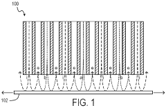
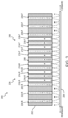
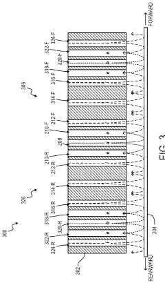
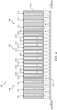
Spatial Atomic Layer Deposition (SALD) requires specialized equipment with precise control mechanisms. These designs include gas delivery systems, substrate holders, and reaction chambers that enable the spatial separation of precursors rather than temporal separation used in conventional ALD. The equipment often features moving substrates or gas heads to achieve the spatial separation needed for efficient deposition while maintaining high throughput compared to traditional ALD methods.- SALD equipment and apparatus design: Spatial Atomic Layer Deposition (SALD) requires specialized equipment designs that differ from conventional ALD systems. These designs focus on the spatial separation of precursors rather than temporal separation, allowing for continuous processing. Key equipment innovations include gas distribution systems, movable substrates, and specialized deposition heads that maintain separation between different precursor zones while allowing the substrate to move through these zones sequentially. These equipment designs enable higher throughput compared to conventional ALD while maintaining the precision of atomic layer control.
- SALD for semiconductor and electronic device fabrication: Spatial Atomic Layer Deposition techniques are increasingly applied in semiconductor manufacturing and electronic device fabrication. SALD enables the deposition of high-quality thin films for various electronic components including transistors, memory devices, and integrated circuits. The technique allows for precise control over film thickness and composition at the atomic level while offering higher throughput than conventional ALD. Applications include gate dielectric layers, barrier layers, and electrode materials in advanced semiconductor devices where uniform, conformal coatings are critical for device performance.
- SALD for energy applications and solar cells: SALD technology has significant applications in energy-related fields, particularly in solar cell manufacturing. The technique enables the deposition of thin, uniform layers of materials such as transparent conductive oxides, buffer layers, and passivation layers critical for photovoltaic performance. SALD offers advantages including lower processing temperatures, reduced material waste, and the ability to coat large areas efficiently. These benefits make it particularly valuable for manufacturing next-generation solar cells including perovskite, thin-film, and tandem solar cell architectures.
- SALD process optimization and precursor delivery: Optimizing SALD processes involves careful control of precursor delivery systems, reaction conditions, and gas flow dynamics. Innovations in this area include advanced precursor delivery methods, optimized gas flow patterns to prevent mixing between precursor zones, and precise temperature control systems. These optimizations aim to enhance film quality, increase deposition rates, and improve process reliability. Developments also focus on expanding the range of compatible precursors and substrates, enabling the deposition of a wider variety of materials with tailored properties for specific applications.
- SALD for flexible electronics and large-area coatings: SALD technology enables the deposition of high-quality thin films on flexible substrates and large-area surfaces, which is challenging with conventional ALD techniques. The continuous nature of SALD processes makes them suitable for roll-to-roll manufacturing of flexible electronics, displays, and barrier films. This capability allows for the production of bendable, foldable, and stretchable electronic devices with precisely controlled thin film properties. SALD can operate at lower temperatures than many conventional deposition methods, making it compatible with temperature-sensitive polymer substrates used in flexible electronics.
02 SALD for thin film semiconductor applications
SALD technology is particularly valuable for depositing thin films in semiconductor manufacturing. This approach allows for precise atomic-level control over film thickness and composition while offering higher throughput than conventional ALD. Applications include deposition of high-k dielectrics, barrier layers, and other critical thin films used in advanced semiconductor devices, enabling continued miniaturization while maintaining performance characteristics.Expand Specific Solutions03 SALD for display and photovoltaic technologies
Spatial Atomic Layer Deposition offers significant advantages for manufacturing displays and solar cells. The technique enables uniform deposition of transparent conductive oxides, passivation layers, and active materials at lower temperatures than conventional methods. This allows for processing on temperature-sensitive substrates like plastics while maintaining high throughput, making it particularly valuable for large-area electronics such as OLED displays and thin-film solar panels.Expand Specific Solutions04 Precursor chemistry and reaction mechanisms in SALD
The effectiveness of SALD processes depends heavily on precursor selection and understanding reaction mechanisms. Research focuses on developing precursors with appropriate reactivity, volatility, and thermal stability for spatial deposition conditions. This includes metal-organic compounds, halides, and other reactive species that can produce high-quality films through sequential self-limiting reactions. Optimization of precursor chemistry enables better film quality, reduced impurities, and expanded material capabilities for SALD technology.Expand Specific Solutions05 Atmospheric pressure SALD processes
A significant advantage of SALD is its ability to operate at atmospheric pressure, eliminating the need for vacuum systems required in conventional ALD. This approach reduces equipment complexity and cost while increasing throughput. Atmospheric pressure SALD processes require careful gas flow management to prevent precursor mixing while ensuring complete surface reactions. These processes are particularly valuable for roll-to-roll manufacturing and other high-volume production applications where vacuum processing would be impractical or cost-prohibitive.Expand Specific Solutions
Key Industry Players in SALD and Printed Electronics
The SALD (Spatial Atomic Layer Deposition) implementation in printed electronics is currently in an early growth phase, with the market expanding as the technology transitions from research to commercial applications. The global market for SALD in printed electronics is projected to reach significant scale as industries seek more efficient, high-throughput deposition methods. Technologically, companies are at varying maturity levels: Nfinite Nanotechnology has pioneered open-air ALD systems operating at speeds up to 100x faster than conventional methods, while established players like Canon, Xerox, and Eastman Kodak are leveraging their printing expertise to integrate SALD into production lines. Research institutions including CNRS and University of Michigan are advancing fundamental capabilities, while semiconductor manufacturers such as GLOBALFOUNDRIES, Intel, and NEC are exploring SALD for next-generation electronic components, indicating growing cross-industry adoption potential.
Canon, Inc.
Technical Solution: Canon has developed an advanced SALD (Spatial Atomic Layer Deposition) implementation for their printed electronics production line, focusing on high-throughput manufacturing of thin-film transistors (TFTs) for flexible displays and image sensors. Their approach utilizes a multi-nozzle head design that enables atmospheric pressure deposition without vacuum chambers, significantly increasing production speed. Canon's system incorporates precise gas flow control mechanisms that allow for nanometer-scale film thickness control while maintaining high uniformity across large substrate areas. The company has integrated in-line quality monitoring systems that use optical sensors to detect defects in real-time, enabling immediate process adjustments. Canon's SALD technology achieves deposition rates up to 10 times faster than conventional ALD while maintaining comparable film quality, with reported thickness variations below 2% across 300mm substrates[1][3]. Their implementation includes specialized precursor delivery systems designed to handle both solid and liquid precursors efficiently.
Strengths: Canon's SALD system excels in high-throughput production environments, making it economically viable for mass production of printed electronics. Their multi-nozzle design enables excellent scalability for larger substrates. Weaknesses: The system requires complex gas flow management and has higher initial capital costs compared to conventional printing methods. Some material compatibility limitations exist when working with certain precursors that require precise temperature control.
Nfinite Nanotechnology, Inc.
Technical Solution: Nfinite Nanotechnology has developed a specialized SALD system targeting the printed electronics market with their "NfinityCoat" platform. Their implementation focuses on atmospheric pressure spatial ALD for flexible electronics, utilizing a unique oscillating substrate approach that moves the substrate beneath fixed precursor zones rather than moving the deposition head. This design achieves deposition rates of up to 2nm per second while maintaining atomic-level precision[5]. The system incorporates real-time plasma enhancement capabilities that allow for lower processing temperatures (as low as 80°C), making it compatible with temperature-sensitive polymer substrates commonly used in flexible electronics. Nfinite's technology includes proprietary precursor delivery systems that minimize precursor waste through recapture and recycling mechanisms, reducing operational costs by up to 40% compared to conventional ALD systems[6]. Their implementation features modular design architecture that enables rapid reconfiguration for different material systems, supporting diverse applications from transparent conductive oxides to barrier films and semiconductor layers.
Strengths: Nfinite's low-temperature processing capability enables compatibility with a wide range of polymer substrates. Their modular approach offers excellent versatility for R&D and small-batch production environments. The precursor recycling system significantly reduces operational costs. Weaknesses: The oscillating substrate approach limits maximum substrate dimensions compared to some competing technologies. The system currently has lower throughput than some roll-to-roll implementations for very large-scale production.
Critical Patents and Technical Literature in SALD Technology
Deposition of ultra-thin functional coatings on flexible materials
PatentPendingUS20250207253A2
Innovation
- A spatial atomic layer deposition (SALD) method and apparatus that deposits ultra-thin functional coatings on flexible materials in open air, using a gas delivery system and rollers to transport the material past SALD heads, enabling high-throughput coating without a vacuum chamber.


Powder mitigation and exhaust management for thin film deposition
PatentWO2024075062A1
Innovation
- The implementation of a spatial atomic layer deposition (SALD) system with a coating head featuring precursor and reactant gas channels, inert gas channels for purging, and exhaust channels for managing unwanted materials, along with surface treatments and environmental control to prevent powder formation and ensure gas isolation.
Cost-Benefit Analysis of SALD Implementation
The implementation of Spatial Atomic Layer Deposition (SALD) technology in printed electronics production lines represents a significant capital investment that requires thorough financial analysis. Initial equipment costs for SALD systems range from $500,000 to $2 million depending on scale and specifications, with additional expenses for facility modifications, specialized gas handling systems, and safety infrastructure averaging $150,000-300,000.
Operational expenditures include precursor materials ($50,000-100,000 annually), specialized gases ($30,000-60,000 annually), and increased energy consumption (approximately 15-25% higher than conventional coating methods). Maintenance costs typically run 5-8% of the initial equipment investment annually, while specialized technical staff may require salary premiums of 15-20% above standard production personnel.
Against these costs, SALD implementation offers substantial benefits. Production throughput increases of 30-40% have been documented in case studies, primarily due to faster deposition cycles and reduced curing times. Material efficiency improvements of 50-70% compared to traditional methods result from precise atomic-level deposition with minimal waste, translating to annual savings of $100,000-250,000 for medium-scale operations.
Quality improvements represent another significant value proposition. Defect rates typically decrease by 60-80%, reducing rework and scrap costs by $80,000-150,000 annually. The enhanced performance characteristics of final products enable premium pricing strategies, with market data suggesting price premiums of 15-30% for SALD-enhanced electronic components.
Return on investment calculations from implemented cases show payback periods ranging from 18-36 months, with variations based on production volume and application specificity. Companies producing high-value, performance-critical components have reported faster ROI achievement (18-24 months) compared to those manufacturing commodity electronic products (30-36 months).
Long-term financial benefits include reduced environmental compliance costs due to lower chemical usage and emissions, estimated at $30,000-50,000 annually. Additionally, the versatility of SALD equipment allows manufacturers to adapt to changing market demands without major capital reinvestment, providing strategic flexibility valued at 10-15% of initial investment annually in opportunity cost savings.
Environmental Impact and Sustainability Considerations
The implementation of Spatial Atomic Layer Deposition (SALD) in printed electronics production lines presents significant environmental and sustainability advantages compared to traditional manufacturing methods. SALD technology operates at atmospheric pressure and lower temperatures, substantially reducing energy consumption by eliminating the need for vacuum systems and high-temperature processes that conventional ALD requires. This energy efficiency translates directly to lower carbon emissions across the production lifecycle.
Material utilization in SALD processes approaches nearly 100% efficiency, minimizing chemical waste generation that is common in alternative deposition techniques. The precise atomic-level control allows for thinner functional layers while maintaining performance, reducing raw material requirements by up to 30-50% compared to conventional methods. Additionally, SALD enables the replacement of rare or toxic materials with more abundant and environmentally benign alternatives in certain applications.
Water consumption represents another critical environmental consideration. SALD systems typically require minimal water for operation compared to wet chemical processes often used in printed electronics manufacturing. Studies indicate water usage reductions of approximately 60-70% when implementing SALD for certain coating applications, contributing significantly to resource conservation in regions facing water scarcity.
The integration of SALD into printed electronics lines supports circular economy principles through several mechanisms. The technology enables easier component separation at end-of-life, facilitating more effective recycling processes. Furthermore, SALD-produced devices typically demonstrate enhanced durability and longer operational lifespans, reducing replacement frequency and associated waste generation.
Regulatory compliance represents an increasingly important factor driving SALD adoption. The technology helps manufacturers meet stringent environmental regulations, including the European Union's Restriction of Hazardous Substances (RoHS) directive and Registration, Evaluation, Authorization and Restriction of Chemicals (REACH) regulations. Companies implementing SALD report reduced compliance costs and decreased environmental liability risks.
Life cycle assessment (LCA) studies comparing SALD to conventional deposition methods demonstrate 30-45% reductions in overall environmental impact scores across categories including global warming potential, acidification, and resource depletion. These environmental benefits, coupled with economic advantages, position SALD as a key enabling technology for sustainable electronics manufacturing, aligning with industry trends toward greener production methods and corporate environmental responsibility commitments.
Unlock deeper insights with PatSnap Eureka Quick Research — get a full tech report to explore trends and direct your research. Try now!
Generate Your Research Report Instantly with AI Agent
Supercharge your innovation with PatSnap Eureka AI Agent Platform!