Analysis of Semiconductor Materials in Neuromorphic Computing
OCT 27, 20259 MIN READ
Generate Your Research Report Instantly with AI Agent
Patsnap Eureka helps you evaluate technical feasibility & market potential.
Neuromorphic Computing Semiconductor Evolution and Objectives
Neuromorphic computing represents a paradigm shift in computational architecture, drawing inspiration from the human brain's neural networks to create more efficient and powerful computing systems. The evolution of semiconductor materials in this field has been marked by significant milestones that have shaped our understanding and implementation of brain-inspired computing technologies.
The journey began in the late 1980s with Carver Mead's pioneering work on neuromorphic engineering, which laid the foundation for hardware implementations of neural networks. Traditional silicon-based CMOS technology initially dominated the field, offering a familiar platform for early neuromorphic designs. However, these conventional materials presented limitations in mimicking the brain's energy efficiency and parallel processing capabilities.
The 2000s witnessed a transition toward specialized semiconductor materials designed specifically for neuromorphic applications. Phase-change materials (PCMs), resistive random-access memory (RRAM), and ferroelectric materials emerged as promising candidates for implementing synaptic functions. These materials offered advantages in non-volatility, scalability, and power efficiency compared to traditional CMOS implementations.
A significant breakthrough came with the development of memristive devices in the 2010s. These two-terminal devices, whose resistance changes based on the history of applied voltage, provided a more accurate analog to biological synapses. Materials such as tantalum oxide, hafnium oxide, and various metal oxides demonstrated the ability to maintain multiple resistance states, enabling more complex neuromorphic functionalities.
Recent years have seen the exploration of two-dimensional materials like graphene and transition metal dichalcogenides (TMDs), which offer exceptional electrical properties at nanoscale dimensions. These materials provide opportunities for creating ultra-thin, flexible neuromorphic devices with unprecedented energy efficiency and integration density.
The primary objective in neuromorphic semiconductor development is to bridge the efficiency gap between biological and artificial neural systems. While the human brain operates on approximately 20 watts of power, comparable artificial systems require orders of magnitude more energy. Developing materials that can support massively parallel, low-power computation remains a central goal.
Another critical objective is achieving true synaptic plasticity in hardware. This requires materials that can exhibit analog behavior with multiple stable states, facilitating learning and memory functions similar to biological systems. The ideal neuromorphic semiconductor would combine high switching speed, low energy consumption, long retention time, and high endurance.
Looking forward, the field aims to develop integrated neuromorphic systems that combine sensing, processing, and memory functions in unified architectures. This will require novel semiconductor materials that can support heterogeneous integration while maintaining compatibility with existing fabrication processes.
Market Analysis for Brain-Inspired Computing Solutions
The neuromorphic computing market is experiencing significant growth, driven by increasing demand for AI applications that require more efficient and brain-like processing capabilities. Current market valuations place the global neuromorphic computing sector at approximately 3.2 billion USD in 2023, with projections indicating a compound annual growth rate of 23.7% through 2030. This remarkable growth trajectory is fueled by expanding applications across autonomous vehicles, robotics, healthcare diagnostics, and edge computing devices.
Market segmentation reveals distinct categories within brain-inspired computing solutions. Hardware-focused segments include neuromorphic chips, memristive systems, and specialized neural processing units, collectively representing about 65% of the current market value. Software and algorithm development accounts for roughly 25%, while services and integration solutions comprise the remaining 10%. This distribution highlights the hardware-centric nature of current market investments.
Industry adoption patterns demonstrate varying levels of market penetration across sectors. Defense and aerospace industries lead implementation with approximately 28% market share, followed by healthcare (22%), automotive (17%), consumer electronics (15%), and industrial automation (12%). The remaining percentage is distributed among emerging application areas including smart cities and IoT ecosystems.
Regional analysis indicates North America currently dominates the market with 42% share, followed by Europe (27%), Asia-Pacific (24%), and other regions (7%). However, the Asia-Pacific region is demonstrating the fastest growth rate at 26.3% annually, primarily driven by substantial investments from China, Japan, and South Korea in semiconductor manufacturing and neuromorphic research initiatives.
Key market drivers include the exponential growth in data generation requiring more efficient processing solutions, increasing demand for edge computing capabilities, and the limitations of traditional von Neumann computing architectures for AI workloads. Additionally, energy efficiency concerns are pushing organizations toward neuromorphic solutions that offer significant power consumption advantages, with some implementations demonstrating 100-1000x improvements in energy efficiency compared to conventional computing systems.
Market challenges include high development costs, technical complexity in designing and manufacturing specialized semiconductor materials, and the need for new programming paradigms. The lack of standardization across neuromorphic platforms also presents integration challenges for potential adopters, creating market entry barriers for smaller players and slowing widespread implementation.
Current Semiconductor Materials Landscape and Barriers
The semiconductor landscape for neuromorphic computing is currently dominated by traditional CMOS (Complementary Metal-Oxide-Semiconductor) technology, which has been adapted to implement neural network architectures. Silicon-based materials remain the foundation for most neuromorphic chips, with companies like Intel (Loihi), IBM (TrueNorth), and BrainChip (Akida) leveraging advanced silicon processes. However, conventional CMOS technology faces fundamental limitations in truly mimicking brain-like computation due to its binary nature and von Neumann architecture constraints.
Emerging materials showing promise include phase-change materials (PCMs) like Ge2Sb2Te5, which can store multiple states in a single device, enabling analog computation. Resistive Random Access Memory (RRAM) materials, particularly metal oxides like HfO2 and TiO2, demonstrate excellent switching characteristics for synaptic weight implementation. Ferroelectric materials such as HfZrO2 are gaining attention for their non-volatile properties and low power consumption characteristics.
Significant barriers exist in the integration of these novel materials with standard CMOS fabrication processes. Compatibility issues arise when attempting to incorporate these materials into existing semiconductor manufacturing lines, often requiring specialized deposition techniques and thermal budget considerations. The reliability and endurance of emerging materials present another major challenge, as neuromorphic systems require components that can withstand millions of switching cycles without significant degradation.
Scaling remains a critical barrier, with many promising materials demonstrating excellent properties at laboratory scale but facing significant challenges in mass production. Variability between devices is particularly problematic for neuromorphic applications, where consistent behavior across millions of artificial synapses is essential for predictable network performance.
Power consumption continues to be a fundamental limitation. While the brain operates at approximately 20 watts, current neuromorphic implementations require significantly more power per equivalent computation. This energy gap stems partly from the inherent properties of semiconductor materials used and the supporting circuitry required.
The thermal management of dense neuromorphic arrays presents another material-related challenge. As device density increases, heat dissipation becomes critical, requiring innovations in both materials and architectural design. Current semiconductor packaging technologies are often inadequate for the three-dimensional integration that would be optimal for neural network implementation.
Manufacturing yield issues compound these challenges, as complex material stacks with multiple interfaces increase the probability of defects. The cost implications of specialized materials and processes also present market barriers to widespread adoption, limiting commercial viability despite promising research results.
Existing Semiconductor Material Solutions for Neural Networks
01 Silicon-based semiconductor materials
Silicon is one of the most widely used semiconductor materials due to its abundance, stability, and suitable electronic properties. Silicon-based semiconductors form the foundation of modern electronics, including integrated circuits, transistors, and solar cells. Various processing techniques are employed to enhance silicon's properties, such as doping with specific elements to control conductivity and creating silicon compounds to improve performance characteristics.- Silicon-based semiconductor materials: Silicon is one of the most widely used semiconductor materials due to its abundance, stability, and suitable electronic properties. Silicon-based semiconductors form the foundation of modern electronics, including integrated circuits, microprocessors, and various electronic devices. These materials can be doped with specific elements to enhance their conductivity and performance characteristics, making them versatile for different applications in the semiconductor industry.
- Compound semiconductor materials: Compound semiconductors are materials formed by combining elements from different groups of the periodic table, such as gallium arsenide (GaAs), gallium nitride (GaN), and indium phosphide (InP). These materials often exhibit superior electronic properties compared to silicon, including higher electron mobility and direct bandgaps, making them ideal for high-frequency applications, optoelectronics, and power devices. Their unique properties enable the development of advanced electronic and photonic devices.
- Semiconductor material manufacturing processes: Various manufacturing processes are employed to produce semiconductor materials with specific properties and structures. These include crystal growth techniques like Czochralski process for silicon ingots, epitaxial growth methods for thin films, and chemical vapor deposition for compound semiconductors. Advanced processing techniques ensure high purity levels and precise control over material composition, which are critical for semiconductor device performance and reliability.
- Novel semiconductor materials and structures: Research in semiconductor materials has led to the development of novel materials and structures with enhanced properties. These include two-dimensional materials like graphene, transition metal dichalcogenides, quantum dots, and nanowires. These innovative materials offer unique electronic, optical, and mechanical properties that can potentially overcome the limitations of conventional semiconductors, enabling new applications in electronics, photonics, and quantum computing.
- Semiconductor materials for specific applications: Specialized semiconductor materials are developed for specific applications such as photovoltaics, power electronics, sensors, and optoelectronic devices. These materials are engineered with properties tailored to their intended use, such as specific bandgaps for solar cells, high breakdown voltages for power devices, or particular optical properties for light-emitting diodes and photodetectors. The selection and optimization of semiconductor materials significantly impact the performance and efficiency of these application-specific devices.
02 Compound semiconductor materials
Compound semiconductors consist of two or more elements combined to create materials with unique electronic properties. These include III-V compounds (like gallium arsenide and indium phosphide) and II-VI compounds (like cadmium telluride). Compound semiconductors often offer advantages over silicon in specific applications, such as higher electron mobility, direct bandgaps for efficient light emission, and better performance at high frequencies and temperatures.Expand Specific Solutions03 Semiconductor manufacturing processes
Various manufacturing processes are employed to produce semiconductor materials with desired properties. These include crystal growth techniques like Czochralski process for silicon ingots, epitaxial growth for thin films, and chemical vapor deposition for compound semiconductors. Advanced processing methods such as lithography, etching, and ion implantation are used to create complex semiconductor structures with precise specifications for electronic devices.Expand Specific Solutions04 Novel semiconductor materials and applications
Research into novel semiconductor materials focuses on enhancing performance beyond traditional silicon technology. This includes wide-bandgap semiconductors like silicon carbide and gallium nitride for power electronics, two-dimensional materials like graphene for flexible electronics, and organic semiconductors for low-cost applications. These materials enable new applications in renewable energy, quantum computing, and advanced sensing technologies.Expand Specific Solutions05 Semiconductor material characterization and testing
Characterization and testing of semiconductor materials are essential for quality control and performance optimization. Various analytical techniques are employed, including X-ray diffraction for crystal structure analysis, scanning electron microscopy for surface morphology, and electrical measurements for determining carrier concentration and mobility. Advanced testing methods ensure semiconductor materials meet specifications for their intended applications in electronic devices.Expand Specific Solutions
Leading Organizations in Neuromorphic Semiconductor Research
Neuromorphic computing is currently in an early growth phase, with the market expected to expand significantly from its current modest size due to increasing applications in AI and edge computing. The technology maturity varies across players, with established semiconductor giants like Samsung Electronics, IBM, and TSMC leading commercial development through significant R&D investments. Academic institutions including Peking University and Fudan University are advancing fundamental research, while specialized companies like Syntiant are developing application-specific neuromorphic chips. The competitive landscape shows a collaborative ecosystem where major semiconductor manufacturers provide fabrication capabilities while research institutions and specialized firms focus on innovative architectures and materials development.
Samsung Electronics Co., Ltd.
Technical Solution: Samsung has developed comprehensive neuromorphic computing solutions based on their expertise in memory technologies and semiconductor manufacturing. Their approach centers on leveraging advanced memory architectures, particularly their High Bandwidth Memory (HBM) and Processing-in-Memory (PIM) technologies, to overcome the von Neumann bottleneck that limits conventional computing for neural network applications. Samsung's neuromorphic research focuses on integrating computation capabilities directly into memory arrays, allowing for massive parallelism similar to biological neural networks. They have pioneered the development of specialized RRAM (Resistive Random Access Memory) cells that can function as artificial synapses, storing weights as variable resistance states. Their neuromorphic architecture implements spike-based processing using specialized analog circuits that mimic neuron behavior while maintaining digital compatibility. Samsung has also explored three-dimensional integration of these components, stacking memory and processing elements to maximize interconnect density while minimizing signal transmission distances and power consumption.
Strengths: Samsung's vertical integration across memory, logic, and manufacturing gives them unique capabilities to implement complete neuromorphic systems. Their established production infrastructure enables rapid scaling of novel technologies from research to commercial deployment. Weaknesses: Their strong focus on memory-centric approaches may limit exploration of alternative neuromorphic paradigms, and their commercial priorities sometimes favor incremental improvements over more radical architectural innovations.
International Business Machines Corp.
Technical Solution: IBM has pioneered neuromorphic computing with its TrueNorth and subsequent Brain-inspired chips. Their approach focuses on developing specialized semiconductor materials and architectures that mimic the brain's neural structure. IBM's neuromorphic chips utilize a combination of traditional CMOS technology with novel materials like phase-change memory (PCM) for synaptic functions. Their TrueNorth architecture implements a million digital neurons and 256 million synapses organized into 4,096 neurosynaptic cores. More recently, IBM has explored analog memory devices using chalcogenide-based materials that can maintain multiple resistance states, enabling more efficient synaptic weight storage. Their research also extends to three-dimensional integration of memory and logic elements to overcome the von Neumann bottleneck, allowing for massively parallel processing similar to biological neural networks.
Strengths: IBM's neuromorphic solutions demonstrate exceptional energy efficiency (70mW for TrueNorth) and scalability. Their integration of novel materials with established CMOS processes enables practical manufacturing. Weaknesses: Their digital neuron implementations may not fully capture the analog nature of biological neurons, and the specialized hardware requires custom programming paradigms that differ significantly from conventional computing approaches.
Critical Materials Science Innovations for Brain-Like Computing
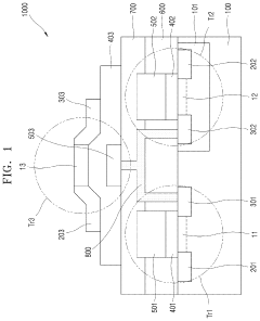
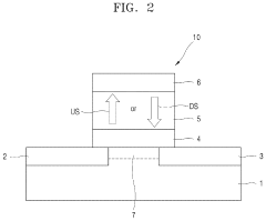
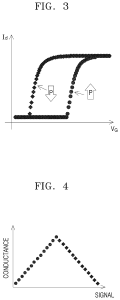
Semiconductor device including ferroelectric material, neuromorphic circuit including the semiconductor device, and neuromorphic computing apparatus including the neuromorphic circuit
PatentActiveUS11887989B2
Innovation
- The development of semiconductor devices and neuromorphic circuits incorporating ferroelectric materials, which enable efficient data processing by simulating synaptic functions, allowing for parallel processing and improved data storage and retrieval, thereby enhancing the accuracy and speed of data processing.
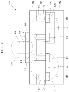
Neuromorphic computing device and method of designing the same
PatentActiveUS11881260B2
Innovation
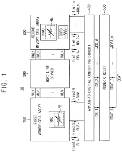
- Incorporating a second memory cell array with offset resistors connected in parallel, using the same resistive material as the first memory cell array, to convert read currents into digital signals, thereby mitigating temperature and time dependency, and ensuring consistent resistance across offset resistors for enhanced sensing performance.
Energy Efficiency Considerations in Neuromorphic Hardware
Energy efficiency represents a critical consideration in the development and implementation of neuromorphic hardware systems. Traditional von Neumann computing architectures face significant energy constraints when processing neural network operations, consuming substantial power due to the constant shuttling of data between memory and processing units. Neuromorphic computing, inspired by the brain's energy-efficient information processing capabilities, aims to overcome these limitations through specialized semiconductor materials and architectures.
The human brain operates on approximately 20 watts of power while performing complex cognitive tasks, a remarkable efficiency that neuromorphic systems seek to emulate. Current neuromorphic hardware implementations demonstrate energy consumption ranging from microwatts to several watts, depending on scale and complexity, representing orders of magnitude improvement over conventional computing approaches for neural processing tasks.
Semiconductor material selection plays a pivotal role in determining the energy profile of neuromorphic systems. Silicon-based CMOS technologies, while well-established, face fundamental thermodynamic limits in energy efficiency. Emerging materials such as phase-change memory (PCM), resistive random-access memory (RRAM), and magnetic tunnel junctions (MTJs) offer promising alternatives with significantly lower energy requirements for synaptic operations, typically in the femtojoule to picojoule range per synaptic event.
The energy advantages of neuromorphic systems derive from several architectural innovations. Event-driven computation, where processing occurs only when necessary rather than at fixed clock cycles, substantially reduces idle power consumption. Local memory-processing integration minimizes data movement energy costs, while analog computation leverages physical properties of materials to perform mathematical operations with minimal energy expenditure.
Thermal management represents another crucial aspect of energy considerations in neuromorphic hardware. Novel cooling solutions and thermally-aware designs are essential for maintaining operational stability, particularly in dense integration scenarios where heat dissipation challenges increase. Three-dimensional integration techniques offer promising pathways to improve energy efficiency through reduced interconnect distances, though they introduce additional thermal management complexities.
Looking forward, the roadmap for energy efficiency in neuromorphic hardware involves exploring ultra-low power semiconductor materials, including 2D materials like graphene and transition metal dichalcogenides, which demonstrate exceptional electrical properties at atomic thicknesses. Additionally, superconducting materials operating at cryogenic temperatures present theoretical energy efficiencies approaching quantum limits, though practical implementation challenges remain substantial.
Manufacturing Scalability of Novel Semiconductor Materials
The scalability of manufacturing processes for novel semiconductor materials represents a critical challenge in advancing neuromorphic computing technologies. Current fabrication methods for traditional silicon-based semiconductors benefit from decades of industrial refinement, while emerging materials for neuromorphic applications often face significant manufacturing hurdles that impede their commercial viability.
Phase-change materials (PCMs) and resistive random-access memory (RRAM) materials show promising characteristics for neuromorphic applications but encounter integration difficulties with conventional CMOS processes. The thermal management requirements of PCMs during fabrication create particular challenges when scaling to high-density arrays, as precise temperature control becomes increasingly difficult across larger wafers.
Oxide-based memristive materials, while demonstrating excellent switching characteristics, suffer from composition variability during large-scale manufacturing. This variability leads to inconsistent device performance across chips and wafers, creating reliability concerns that must be addressed before widespread adoption can occur.
Spin-based materials for neuromorphic computing face even greater manufacturing challenges. Current deposition techniques for magnetic tunnel junctions require atomic-level precision that becomes exponentially more difficult to maintain across larger substrate areas. The yield rates for these advanced materials remain significantly lower than those of conventional semiconductor processes.
Recent advancements in atomic layer deposition (ALD) techniques show promise for improving the manufacturing consistency of complex oxide materials. Several research groups have demonstrated improved stoichiometric control using modified ALD processes, potentially addressing some variability issues. However, these techniques still operate at laboratory scales rather than production volumes.
The economic considerations of scaling novel semiconductor materials cannot be overlooked. Current cost structures for materials like hafnium oxide and tantalum oxide remain substantially higher than silicon, with specialized deposition equipment adding further capital expenses. Industry projections suggest a 3-5 year timeline before manufacturing costs could approach commercially viable levels for neuromorphic applications.
Contamination control presents another significant challenge, as many novel materials demonstrate extreme sensitivity to impurities. Manufacturing environments for these advanced semiconductors require cleanliness levels exceeding those of standard semiconductor fabs, further increasing production costs and complexity.
Cross-industry collaborations between material scientists, process engineers, and equipment manufacturers will be essential to overcome these scalability challenges. Several consortium efforts have emerged recently, focusing specifically on standardizing fabrication processes for neuromorphic materials to accelerate their path to commercial viability.
Unlock deeper insights with Patsnap Eureka Quick Research — get a full tech report to explore trends and direct your research. Try now!
Generate Your Research Report Instantly with AI Agent
Supercharge your innovation with Patsnap Eureka AI Agent Platform!