

Benchmarking Organic Photovoltaics: Material Microstructure vs Performance
SEP 19, 20259 MIN READ
Generate Your Research Report Instantly with AI Agent
PatSnap Eureka helps you evaluate technical feasibility & market potential.
OPV Technology Background and Objectives
Organic photovoltaics (OPVs) have emerged as a promising renewable energy technology since their inception in the 1980s. The evolution of OPVs has been characterized by significant advancements in material science, device architecture, and manufacturing processes. Initially achieving power conversion efficiencies (PCEs) below 1%, modern OPVs now regularly exceed 18% in laboratory settings, demonstrating remarkable progress in a relatively short timeframe compared to traditional photovoltaic technologies.
The fundamental appeal of OPVs lies in their unique combination of properties: mechanical flexibility, lightweight nature, solution processability, and potential for low-cost, high-throughput manufacturing. These attributes position OPVs as complementary to conventional silicon-based photovoltaics rather than direct competitors, opening new application spaces where traditional rigid panels are impractical.
The relationship between material microstructure and device performance represents the central challenge and opportunity in OPV development. Organic semiconducting materials, including conjugated polymers and small molecules, form complex heterogeneous structures at the nanoscale that directly influence charge generation, transport, and collection processes. Understanding and controlling these microstructural features is paramount to optimizing device performance.
Current technical objectives in the OPV field focus on several interconnected goals. First, pushing efficiency boundaries through novel materials and optimized morphologies remains a primary target, with theoretical limits suggesting PCEs above 25% may be achievable. Second, enhancing operational stability and lifetime under real-world conditions presents a critical challenge, as commercial viability demands device longevity comparable to silicon alternatives.
Third, establishing standardized benchmarking protocols for correlating microstructure with performance metrics is essential for accelerating development cycles and enabling meaningful comparisons across research groups. This includes advanced characterization techniques spanning multiple length scales, from molecular ordering to domain formation.
Fourth, scaling production while maintaining performance represents a significant hurdle in translating laboratory successes to commercial products. The sensitivity of OPV performance to processing conditions necessitates precise control over manufacturing parameters at industrial scales.
The trajectory of OPV technology indicates a shift from purely efficiency-focused research toward a more holistic approach that balances multiple performance factors including stability, scalability, and environmental impact. This evolution reflects the maturing nature of the field and its progression toward commercial relevance in specialized energy markets.
Market Analysis for Organic Photovoltaics
The organic photovoltaics (OPV) market has been experiencing significant growth in recent years, driven by increasing demand for renewable energy solutions and advancements in material science. The global OPV market was valued at approximately $87 million in 2022 and is projected to reach $378 million by 2030, growing at a CAGR of 20.1% during the forecast period.
Consumer electronics represents the largest application segment for OPV technology, accounting for nearly 40% of the market share. This dominance is attributed to the lightweight, flexible, and semi-transparent nature of organic solar cells, making them ideal for integration into portable electronic devices. Building-integrated photovoltaics (BIPV) follows as the second-largest segment, with increasing adoption in smart windows, facades, and architectural elements.
Regionally, Europe leads the OPV market with approximately 35% market share, followed by North America and Asia-Pacific. European dominance stems from stringent renewable energy policies and substantial R&D investments. However, the Asia-Pacific region is expected to witness the fastest growth rate due to expanding manufacturing capabilities in China, Japan, and South Korea.
Key market drivers include decreasing production costs, improving power conversion efficiencies (PCEs), and growing environmental consciousness. The cost of OPV modules has declined by approximately 30% over the past five years, enhancing their commercial viability. Additionally, recent breakthroughs in material microstructure have pushed laboratory PCEs beyond 18%, narrowing the gap with traditional silicon-based photovoltaics.
Market challenges persist, primarily related to stability issues, scalability of production, and competition from other emerging photovoltaic technologies. The average operational lifetime of OPV devices remains between 5-7 years, significantly shorter than the 25+ years offered by silicon-based alternatives.
Customer segmentation reveals three primary groups: technology companies seeking power solutions for consumer electronics, construction firms interested in BIPV applications, and utility companies exploring complementary renewable energy sources. Each segment prioritizes different performance metrics, with electronics manufacturers valuing flexibility and weight, while utility companies focus on efficiency and cost per watt.
The competitive landscape features both established players and innovative startups. Heliatek, ASCA, Epishine, and InfinityPV lead in commercialization efforts, while companies like Merck and Sumitomo Chemical dominate the materials supply chain. Strategic partnerships between material developers and device manufacturers have become increasingly common, accelerating the path to market for novel microstructure innovations.
Current Challenges in OPV Microstructure Characterization
Despite significant advancements in organic photovoltaic (OPV) technology, characterizing the microstructure of organic semiconductor materials remains one of the most challenging aspects in the field. Current techniques often struggle to provide comprehensive insights into the complex morphological features that directly influence device performance. The nanoscale phase separation between donor and acceptor materials, critical for efficient exciton dissociation and charge transport, presents particular difficulties for accurate measurement and quantification.
Traditional characterization methods such as atomic force microscopy (AFM) only provide surface topography information, failing to capture the three-dimensional bulk heterojunction architecture that determines device efficiency. Transmission electron microscopy (TEM) offers higher resolution but suffers from poor contrast between organic components with similar electron densities, and sample preparation can inadvertently alter the native microstructure.
X-ray and neutron scattering techniques, while powerful for probing crystallinity and domain sizes, face limitations in distinguishing between amorphous regions that significantly impact charge transport properties. Additionally, these techniques typically provide spatially averaged information, obscuring local variations in morphology that can create performance bottlenecks in devices.
In-situ and operando characterization presents another frontier challenge. Current methods struggle to monitor microstructural evolution during device operation or fabrication processes in real-time, limiting our understanding of degradation mechanisms and morphological stability under working conditions. This knowledge gap hinders the development of strategies to enhance long-term device stability.
Correlating multiple characterization techniques remains problematic due to differences in sample preparation requirements, measurement conditions, and data analysis protocols. Researchers often face difficulties in establishing direct relationships between microstructural features observed through different methods, complicating efforts to build comprehensive morphological models.
Computational challenges further compound these issues. The massive datasets generated by advanced characterization techniques require sophisticated algorithms for interpretation. Current image analysis tools often lack the capability to automatically identify and quantify relevant morphological features across different length scales, from molecular packing to mesoscale domain organization.
Standardization across the field represents another significant hurdle. The absence of universally accepted protocols for sample preparation, measurement conditions, and data analysis makes direct comparisons between studies conducted by different research groups problematic, hampering collaborative progress toward optimized microstructures for high-performance devices.
Benchmarking Methodologies for OPV Performance Evaluation
01 Materials and compositions for improved OPV efficiency
Various materials and compositions can enhance the performance of organic photovoltaics. These include novel donor-acceptor polymers, fullerene derivatives, and non-fullerene acceptors that improve light absorption and charge transport properties. Specific molecular designs and nanostructured materials can optimize band gaps, increase charge mobility, and reduce recombination losses, leading to higher power conversion efficiencies in organic solar cells.- Materials and compositions for improved efficiency: Various materials and compositions can enhance the performance of organic photovoltaics. These include novel organic semiconductors, donor-acceptor combinations, and specialized additives that improve charge transport and light absorption. Optimizing the molecular structure and composition of active layers can significantly increase power conversion efficiency and stability of organic solar cells.
- Device architecture and fabrication techniques: The architecture and fabrication methods of organic photovoltaic devices play crucial roles in their performance. Innovations in layer stacking, interface engineering, and electrode design can minimize energy losses and enhance charge collection. Advanced manufacturing techniques such as solution processing, roll-to-roll fabrication, and precise control of film morphology contribute to higher efficiency and scalability.
- Performance measurement and characterization methods: Accurate measurement and characterization of organic photovoltaic performance are essential for development and optimization. Various techniques are employed to evaluate power conversion efficiency, quantum efficiency, charge carrier mobility, and device stability. Advanced analytical methods help identify performance bottlenecks and guide improvements in material design and device fabrication.
- Stability and lifetime enhancement: Improving the operational stability and lifetime of organic photovoltaics is critical for commercial viability. Approaches include encapsulation techniques, UV filters, antioxidants, and structural modifications that protect against degradation mechanisms such as photo-oxidation, thermal stress, and mechanical damage. Enhanced stability enables organic solar cells to maintain high performance over extended periods under real-world conditions.
- Modeling and simulation for performance prediction: Computational modeling and simulation tools enable prediction and optimization of organic photovoltaic performance. These include quantum mechanical calculations, molecular dynamics simulations, and device physics models that provide insights into charge generation, transport, and recombination processes. Such theoretical approaches accelerate material discovery and device design by reducing the need for extensive experimental testing.
02 Device architecture and fabrication techniques
The performance of organic photovoltaics can be significantly enhanced through optimized device architectures and fabrication methods. Techniques such as bulk heterojunction structures, tandem cell configurations, and interface engineering improve charge separation and collection. Advanced processing methods including solution processing, thermal annealing, and solvent additives control the morphology of the active layer, while buffer layers and electrodes with appropriate work functions enhance charge extraction.Expand Specific Solutions03 Measurement and characterization methods
Accurate measurement and characterization techniques are essential for evaluating and improving organic photovoltaic performance. Methods include current-voltage characterization under standardized illumination conditions, quantum efficiency measurements, impedance spectroscopy, and transient optical techniques. Advanced imaging and spectroscopic tools help analyze morphology, charge carrier dynamics, and degradation mechanisms, enabling researchers to identify performance bottlenecks and optimize device parameters.Expand Specific Solutions04 Stability and lifetime enhancement
Improving the stability and operational lifetime of organic photovoltaics is crucial for commercial viability. Approaches include developing materials resistant to photo-oxidation, encapsulation technologies that prevent moisture and oxygen ingress, and additives that stabilize the morphology of the active layer. Thermal stability enhancements and interface engineering reduce degradation mechanisms, while self-healing materials and protective coatings extend device lifetime under real-world operating conditions.Expand Specific Solutions05 Scalable manufacturing and integration
Scalable manufacturing processes and system integration techniques are essential for commercializing organic photovoltaic technology. Roll-to-roll printing, spray coating, and other high-throughput fabrication methods enable large-area production while maintaining performance. Integration approaches for building-integrated photovoltaics, portable electronics, and IoT applications leverage the flexibility, lightweight nature, and semi-transparency of organic solar cells. Optimization of module design, interconnections, and power management systems maximizes real-world energy yield.Expand Specific Solutions
Leading Companies and Research Institutions in OPV Field
The organic photovoltaics (OPV) market is currently in a transitional phase from research to early commercialization, with a growing market projected to reach $300 million by 2027. Technical maturity varies significantly across players, with research institutions like MIT, University of Michigan, and Chinese Academy of Sciences leading fundamental microstructure research, while companies like Heliatek, Novaled, and Sumitomo Chemical focus on translating these insights into commercial applications. Industry giants including Samsung, Toshiba, and Panasonic are strategically positioned through patent portfolios but face efficiency and stability challenges. The competitive landscape shows a collaborative ecosystem between academic institutions developing novel materials and industrial partners scaling manufacturing processes, with increasing interest from energy companies like Phillips 66 and TotalEnergies seeking diversification into renewable technologies.
The Regents of the University of Michigan
Technical Solution: The University of Michigan has developed a comprehensive benchmarking framework for organic photovoltaics that specifically addresses the relationship between nanoscale morphology and device performance metrics. Their approach centers on multi-modal characterization techniques combined with custom-built in-situ measurement platforms that monitor morphological evolution during processing. Using resonant soft X-ray scattering (R-SoXS) and advanced scanning probe microscopy techniques, their research has quantified domain composition, interfacial mixing, and molecular orientation in high-performance OPV blends. Michigan's benchmarking methodology includes standardized protocols for sample preparation and device fabrication that isolate morphological variables from other performance factors. Their studies have established critical correlations between processing solvents, additive concentrations, and thermal treatments on resulting film microstructure, demonstrating how these parameters directly impact charge generation, recombination, and extraction processes. Recent work has focused on developing machine learning algorithms that can predict optimal processing conditions based on molecular structure inputs, creating a powerful tool for accelerating materials development. Their benchmarking platform has been applied to numerous material systems, creating a valuable database of structure-property relationships across polymer:fullerene and polymer:non-fullerene acceptor combinations.
Strengths: World-class characterization infrastructure specifically optimized for OPV materials; established protocols enabling reliable comparison across material systems; strong integration between device physics and materials science. Weaknesses: Challenges in scaling laboratory fabrication methods to industrial processes; focus primarily on solution-processed systems rather than vacuum-deposited architectures; limited commercial translation of academic findings.
National Research Council of Canada
Technical Solution: The National Research Council of Canada has established a standardized benchmarking protocol for organic photovoltaic materials that systematically correlates microstructural parameters with device performance metrics. Their approach combines advanced characterization techniques with standardized device architectures to isolate material-specific contributions to performance. Using a combination of neutron scattering techniques available at Canadian nuclear facilities and advanced electron microscopy, NRC researchers have developed quantitative methods to assess domain size, purity, and connectivity in OPV active layers. Their benchmarking platform includes environmental testing chambers that simulate real-world operating conditions, allowing correlation between initial microstructure and morphological stability under thermal stress, light exposure, and humidity. NRC has pioneered non-destructive testing methods for OPV modules, correlating manufacturing variations with spatial performance distribution. Their research has established key relationships between polymer crystallinity, fullerene aggregation, and resulting charge transport properties, providing design rules for material optimization. The NRC benchmarking methodology includes round-robin testing between multiple laboratories to ensure reproducibility of results, addressing a critical challenge in the OPV field where processing conditions significantly impact performance.
Strengths: Comprehensive testing infrastructure including environmental chambers and outdoor testing facilities; strong focus on standardization and reproducibility; access to specialized neutron scattering facilities. Weaknesses: More focused on characterization and standardization than novel materials development; challenges in keeping pace with rapidly evolving non-fullerene acceptor systems; limited commercial partnerships compared to industry-led efforts.
Key Microstructure-Performance Relationship Patents
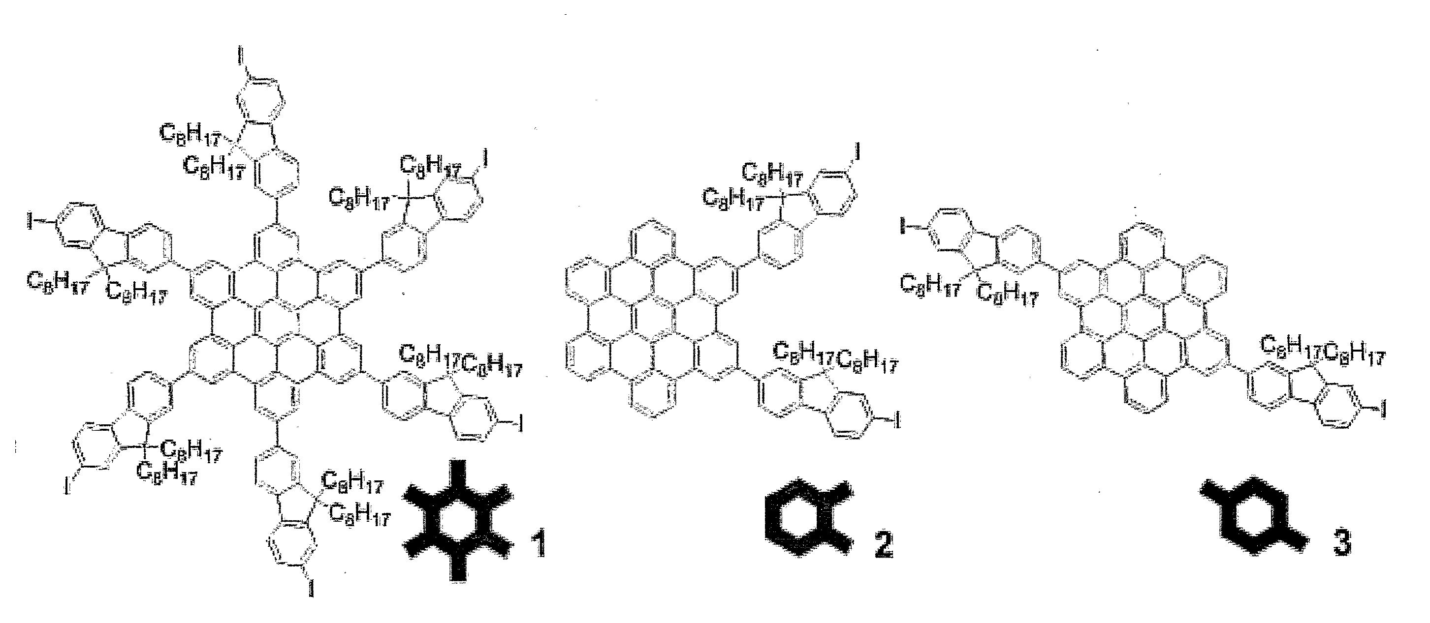
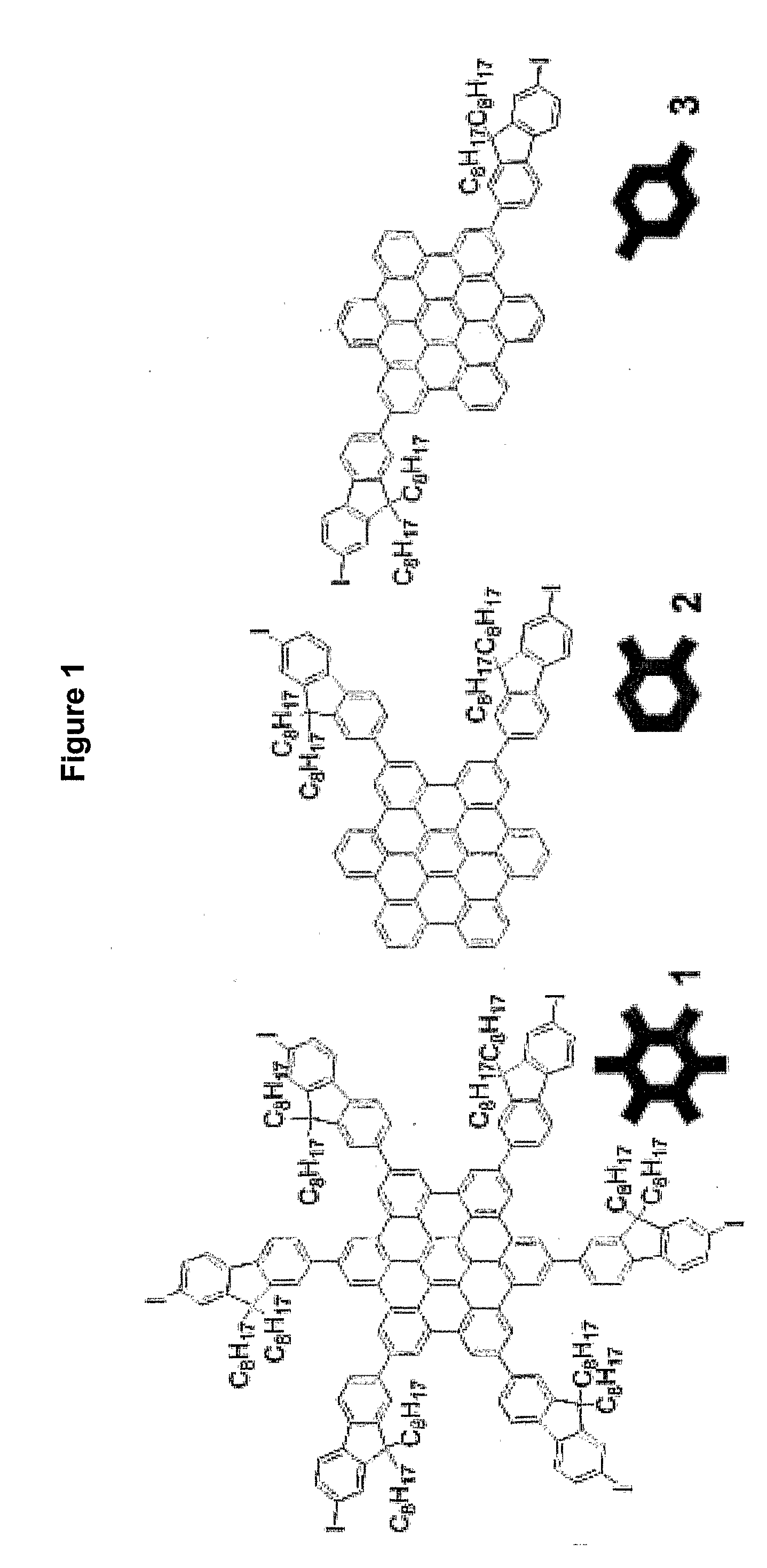
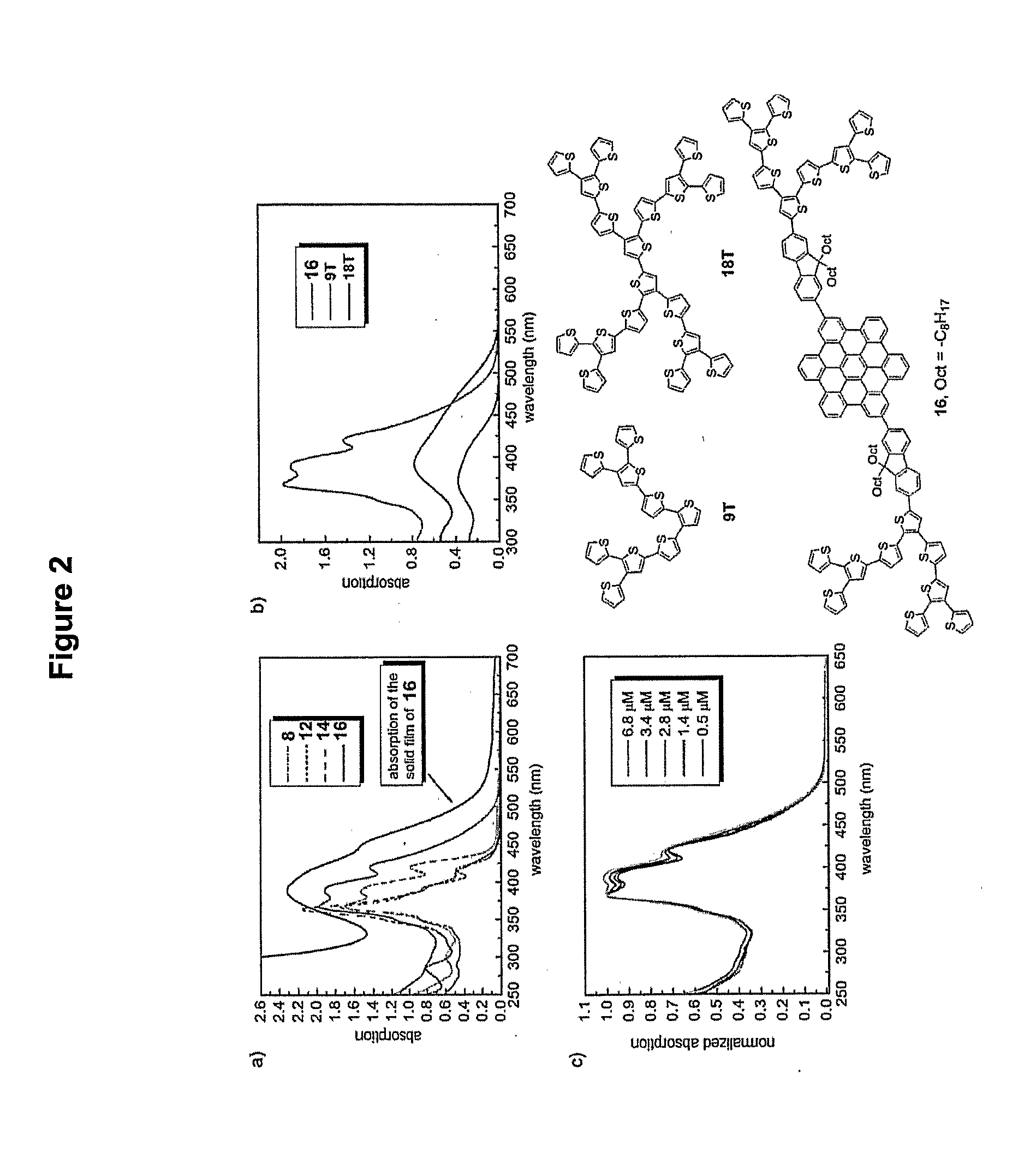
Novel compounds, derivatives thereof and their use in heterojunction devices
PatentInactiveUS20120024382A1
Innovation
- Development of conjugated compounds with a hexabenzocoronene core peripherally substituted with conjugated aromatic or heteroaromatic moieties, which confer solubility and modify charge transport mobility, allowing for the formation of ordered structures in films, such as fluorenyl-substituted HBC derivatives that can be easily functionalized and used in heterojunction devices.

Scalability and Manufacturing Considerations for OPV
The scalability of organic photovoltaics (OPV) represents a critical factor in determining their commercial viability and widespread adoption. Current laboratory-scale fabrication techniques, while effective for research purposes, face significant challenges when transitioning to industrial-scale production. Roll-to-roll (R2R) processing emerges as the most promising manufacturing approach for OPV, offering high throughput and continuous production capabilities essential for cost-effective scaling.
Material considerations play a pivotal role in manufacturing scalability. The microstructure-performance relationship becomes increasingly complex at larger scales, where maintaining consistent morphology across large areas presents substantial challenges. Variations in film thickness, molecular orientation, and domain size can lead to performance inconsistencies across modules. Recent advances in solution engineering and additive control have improved homogeneity in large-area films, though further optimization remains necessary.
Process compatibility represents another crucial aspect of OPV manufacturing. Traditional laboratory techniques often employ toxic solvents that pose environmental and safety concerns at industrial scales. The transition toward green solvents and water-based processing has shown promising results, with recent studies demonstrating comparable efficiencies using environmentally benign alternatives. However, these approaches frequently require modifications to material design and process parameters to maintain optimal microstructure formation.
Encapsulation technology constitutes a significant manufacturing consideration that directly impacts device lifetime and stability. The correlation between material microstructure and barrier requirements necessitates tailored encapsulation strategies. Multi-layer barrier films with alternating organic and inorganic layers have demonstrated superior performance in protecting sensitive OPV microstructures from oxygen and moisture degradation while maintaining flexibility.
Cost analysis reveals that material synthesis currently represents approximately 40-50% of total manufacturing expenses for OPV. Economies of scale could potentially reduce these costs, but material design strategies that simplify synthesis pathways while maintaining performance metrics would provide more immediate benefits. Recent developments in high-yielding synthetic routes and reduced purification requirements offer promising directions for cost reduction.
Quality control methodologies for large-scale production require non-destructive, in-line characterization techniques capable of monitoring microstructural parameters during manufacturing. Advanced optical methods including in-situ Raman spectroscopy and polarized light imaging have demonstrated capability for real-time monitoring of crystallization dynamics and domain formation, enabling process adjustments to maintain optimal microstructure across production runs.
Environmental Impact and Sustainability of OPV Technologies
Organic Photovoltaics (OPVs) represent a significant advancement in sustainable energy technology, offering environmental benefits that extend beyond traditional silicon-based solar cells. The environmental impact assessment of OPVs reveals substantially lower carbon footprints during manufacturing processes compared to conventional photovoltaics. Life cycle analyses indicate that OPVs require less energy input during production, with energy payback times potentially as short as a few months in optimal conditions, compared to 1-2 years for silicon-based alternatives.
Material composition of OPVs presents both advantages and challenges from a sustainability perspective. The carbon-based materials used in OPVs are abundant and can be derived from renewable resources, reducing dependence on rare or geographically concentrated elements. However, certain high-performance OPV formulations incorporate fullerene derivatives and specialized dopants that may present end-of-life management challenges.
The flexibility and lightweight nature of OPV technologies enable integration into existing structures without requiring additional supporting infrastructure, thereby reducing overall material consumption. This characteristic also facilitates transportation efficiency, further decreasing the carbon footprint associated with deployment. Additionally, the potential for roll-to-roll manufacturing processes significantly reduces energy consumption during production compared to the high-temperature processes required for inorganic photovoltaics.
End-of-life considerations for OPVs demonstrate promising recyclability pathways. Research indicates that up to 90% of organic materials can be recovered through appropriate solvent-based recycling processes. However, the composite nature of OPV devices, which often incorporate multiple thin layers of different materials, presents technical challenges for complete material separation and recovery.
Water usage metrics for OPV manufacturing show substantial improvements over silicon-based technologies, with some studies indicating up to 95% reduction in water consumption throughout the production lifecycle. This aspect becomes increasingly important as water scarcity concerns grow globally, particularly in regions with high solar potential.
Toxicity assessments of OPV materials reveal mixed results. While many organic semiconductors demonstrate low acute toxicity, the long-term environmental persistence and bioaccumulation potential of novel conjugated polymers remain under investigation. Recent advancements in green chemistry approaches have yielded non-toxic solvent systems and environmentally benign processing methods that significantly reduce hazardous waste generation during manufacturing.
The correlation between material microstructure and environmental impact presents an emerging research direction. Optimizing molecular arrangements not only improves device performance but can enhance material stability, potentially extending operational lifetimes and improving sustainability metrics. This relationship between nanoscale morphology and macroscale environmental benefits represents a critical frontier in sustainable OPV development.
Unlock deeper insights with PatSnap Eureka Quick Research — get a full tech report to explore trends and direct your research. Try now!
Generate Your Research Report Instantly with AI Agent
Supercharge your innovation with PatSnap Eureka AI Agent Platform!