

What Are the Challenges in Commercializing 2D Semiconductor Heterostructures?
OCT 21, 20259 MIN READ
Generate Your Research Report Instantly with AI Agent
PatSnap Eureka helps you evaluate technical feasibility & market potential.
2D Semiconductor Evolution and Commercialization Goals
Two-dimensional (2D) semiconductors have emerged as a revolutionary class of materials since the isolation of graphene in 2004. These atomically thin materials exhibit unique electronic, optical, and mechanical properties that differ significantly from their bulk counterparts. The evolution of 2D semiconductors has progressed through several distinct phases, beginning with graphene exploration, followed by the discovery of transition metal dichalcogenides (TMDs) such as MoS2 and WS2, and more recently expanding to include diverse materials like hexagonal boron nitride (h-BN), black phosphorus, and MXenes.
The technological trajectory has been marked by significant breakthroughs in synthesis methods, transitioning from mechanical exfoliation to more scalable approaches including chemical vapor deposition (CVD), molecular beam epitaxy (MBE), and solution-based processes. This evolution has gradually improved material quality, consistency, and production scale, though significant challenges remain in achieving industrial-grade uniformity and reproducibility.
Heterostructures—combinations of different 2D materials stacked vertically or connected laterally—represent the frontier of 2D semiconductor development. These structures enable unprecedented control over electronic band structures and quantum phenomena, potentially revolutionizing next-generation electronics, optoelectronics, and quantum computing devices.
The commercialization goals for 2D semiconductor heterostructures span multiple industries. In electronics, objectives include developing high-performance field-effect transistors with superior mobility and switching characteristics to overcome silicon's physical limitations. For optoelectronics, the aim is to create efficient light-emitting diodes, photodetectors, and photovoltaic cells leveraging the direct bandgaps and strong light-matter interactions of 2D materials.
Quantum technologies represent another critical commercialization target, with 2D heterostructures offering promising platforms for single-photon emitters, quantum bits, and quantum sensors. Additionally, energy storage applications seek to exploit the high surface-to-volume ratio and unique electronic properties of these materials for next-generation batteries and supercapacitors.
The timeline for commercialization varies by application, with simpler implementations in sensing and photonics potentially reaching market within 3-5 years, while more complex electronic applications may require 7-10 years of further development. The ultimate goal is to establish 2D semiconductor heterostructures as a viable platform that complements or potentially replaces conventional semiconductor technologies in specific high-value applications where their unique properties offer decisive advantages.
Market Demand Analysis for 2D Heterostructure Applications
The global market for 2D semiconductor heterostructures is experiencing significant growth, driven by increasing demand for miniaturized electronic components with enhanced performance capabilities. Current market projections indicate that the 2D materials market, including heterostructures, is expected to grow at a compound annual growth rate of over 30% through 2030, with particular acceleration in electronics and optoelectronics applications.
The demand for 2D heterostructures is primarily concentrated in several key sectors. In the semiconductor industry, there is growing interest in these materials as potential solutions for extending Moore's Law beyond traditional silicon limitations. The unique electronic properties of 2D heterostructures, including high carrier mobility and tunable bandgaps, make them attractive candidates for next-generation transistors and integrated circuits.
Telecommunications and data processing represent another significant market segment. The superior electron transport properties of certain 2D heterostructures enable faster switching speeds and lower power consumption, addressing critical needs in high-performance computing and data centers where energy efficiency is paramount.
The optoelectronics sector demonstrates particularly strong demand growth, with applications in photodetectors, light-emitting diodes, and photovoltaic cells. Market research indicates that the integration of 2D heterostructures in these devices can potentially improve efficiency by 20-40% compared to conventional materials, creating substantial value propositions for manufacturers.
Energy storage represents an emerging application area with considerable market potential. Research indicates that 2D heterostructures can significantly enhance the performance of batteries and supercapacitors, potentially addressing key limitations in current energy storage technologies. This aligns with the growing global focus on renewable energy and electrification.
Geographically, North America and East Asia currently dominate market demand, with Europe showing accelerated growth in research applications. China has emerged as a particularly aggressive market player, with substantial government investment in both research and commercialization infrastructure for 2D materials.
Despite strong technological interest, the actual commercial market remains nascent. Current market analysis reveals a significant gap between laboratory demonstrations and commercial-scale production capabilities. End-user industries express strong interest in the potential performance advantages but remain cautious about adoption due to manufacturing scalability concerns and cost considerations.
Market surveys indicate that price sensitivity varies significantly by application sector. While consumer electronics manufacturers prioritize cost competitiveness, specialized applications in aerospace, defense, and scientific instrumentation demonstrate willingness to accept premium pricing for performance advantages, creating potential early-adoption market niches.
Technical Barriers in 2D Semiconductor Heterostructure Development
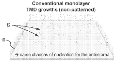
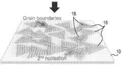
The development of 2D semiconductor heterostructures faces significant technical barriers that currently impede widespread commercialization. One of the primary challenges lies in the scalable synthesis of high-quality 2D materials with consistent properties. Current methods like mechanical exfoliation produce high-quality flakes but are inherently non-scalable for industrial applications. Chemical vapor deposition (CVD) offers better scalability but struggles with uniformity across large areas and introduces defects that compromise electrical performance.
Interface engineering presents another formidable obstacle. When creating heterostructures by stacking different 2D materials, controlling the interface quality becomes critical. Contamination, lattice mismatches, and trapped impurities at these interfaces can significantly degrade device performance. The atomically thin nature of these materials makes them extremely sensitive to environmental factors, requiring precise control during fabrication processes.
Contact resistance remains a persistent challenge that limits device performance. The atomically thin nature of 2D materials creates unique difficulties in forming low-resistance electrical contacts, as traditional metallization techniques often damage the delicate 2D layers or create Schottky barriers that impede carrier transport. This issue becomes even more complex in heterostructure devices where multiple material interfaces must be considered.
Encapsulation and passivation technologies are underdeveloped for 2D heterostructures. These materials are highly susceptible to degradation from oxygen, moisture, and other environmental factors. Current encapsulation methods often introduce additional defects or alter the intrinsic properties of the 2D materials, compromising device performance and reliability.
Integration with existing semiconductor manufacturing infrastructure presents significant compatibility issues. The temperature sensitivities, handling requirements, and process chemistries of 2D materials often conflict with established CMOS fabrication processes. This incompatibility creates substantial barriers to incorporating these novel materials into existing manufacturing lines.
Metrology and characterization techniques for 2D heterostructures remain inadequate for industrial quality control. The atomically thin nature of these materials requires specialized tools and methodologies to accurately assess layer quality, interface properties, and defect densities at production scales. Current techniques are often destructive, time-consuming, or lack the spatial resolution needed for effective quality control.
Thermal management issues also plague 2D heterostructure devices. The thermal conductivity anisotropy in these materials creates unique heat dissipation challenges that can lead to performance degradation and reliability concerns in high-power applications. Developing effective thermal management solutions while maintaining the advantageous properties of 2D materials remains an unsolved engineering challenge.
Current Manufacturing Solutions for 2D Heterostructures
01 Manufacturing scalability challenges
The commercialization of 2D semiconductor heterostructures faces significant manufacturing scalability challenges. Current production methods often struggle with consistent large-scale fabrication, maintaining uniform quality across wafers, and achieving high throughput necessary for commercial viability. These challenges include difficulties in controlling layer thickness, ensuring atomically clean interfaces between different 2D materials, and developing equipment suitable for industrial-scale production while maintaining the exceptional electronic properties that make these materials valuable.- Manufacturing scalability challenges: The commercialization of 2D semiconductor heterostructures faces significant manufacturing scalability challenges. Current production methods often struggle with consistent large-scale fabrication, maintaining uniform quality across wafers, and achieving cost-effective production rates. The transition from laboratory-scale production to industrial manufacturing requires overcoming issues related to defect control, layer alignment precision, and reproducibility of electrical and optical properties across batches.
- Integration with existing semiconductor technologies: A major commercialization challenge involves integrating 2D semiconductor heterostructures with conventional semiconductor technologies and manufacturing processes. This includes compatibility issues with standard CMOS processes, thermal budget constraints, and interface engineering between 2D materials and 3D substrates. The development of hybrid integration approaches that leverage existing infrastructure while accommodating the unique properties of 2D materials remains a significant technical hurdle.
- Material quality and consistency barriers: Achieving consistent material quality in 2D semiconductor heterostructures presents substantial commercialization challenges. Issues include controlling the number of layers, minimizing contamination during transfer processes, managing interfacial defects between different 2D materials, and ensuring batch-to-batch consistency. The sensitivity of 2D materials to environmental factors during processing and the difficulty in characterizing atomic-level defects further complicate quality control efforts.
- Economic and market adoption challenges: The commercialization of 2D semiconductor heterostructures faces economic challenges related to high production costs, uncertain return on investment, and market adoption barriers. The specialized equipment and expertise required for production, coupled with competition from established technologies, create significant market entry barriers. Additionally, the need for ecosystem development, including specialized design tools, testing protocols, and supply chain infrastructure, further complicates commercial viability.
- Performance reliability and device lifetime issues: Long-term reliability and performance stability present critical challenges for 2D semiconductor heterostructure commercialization. These materials often exhibit sensitivity to environmental factors such as oxygen, moisture, and temperature fluctuations, which can degrade performance over time. Addressing encapsulation requirements, contact degradation, and operational stability under various conditions is essential for commercial applications. The development of standardized reliability testing protocols specific to 2D materials remains an ongoing challenge.
02 Integration with existing semiconductor technologies
A major commercialization challenge involves integrating 2D semiconductor heterostructures with conventional semiconductor technologies and manufacturing processes. This includes compatibility issues with silicon-based platforms, thermal budget constraints during processing, contact resistance problems at metal-2D material interfaces, and developing appropriate encapsulation techniques to protect the sensitive 2D materials from environmental degradation. Successful commercialization requires seamless integration with existing fabrication infrastructure to leverage established supply chains.Expand Specific Solutions03 Material quality and consistency barriers
Achieving consistent material quality presents significant obstacles to commercialization. Issues include controlling defect densities, ensuring batch-to-batch reproducibility, and maintaining crystalline quality during transfer processes. The properties of 2D semiconductor heterostructures are highly sensitive to atomic-level defects, contamination, and strain, which can dramatically alter their electronic and optical characteristics. Developing standardized quality metrics and reliable characterization techniques is essential for industrial adoption and quality assurance in commercial applications.Expand Specific Solutions04 Economic and market entry challenges
Economic factors significantly impact the commercialization of 2D semiconductor heterostructures. These include high initial production costs, uncertain return on investment timelines, intellectual property complexities, and competition from established technologies. Market entry requires identifying appropriate applications where the unique properties of 2D heterostructures provide sufficient value to justify premium pricing. Additionally, establishing supply chains for specialized materials and equipment presents logistical and financial hurdles that must be overcome for successful commercialization.Expand Specific Solutions05 Device reliability and performance stability
Long-term reliability and performance stability of devices based on 2D semiconductor heterostructures remain significant commercialization challenges. These materials often exhibit sensitivity to environmental factors such as oxygen, moisture, and temperature fluctuations, which can degrade performance over time. Additionally, interface stability between different 2D materials in heterostructures can change during operation, affecting device characteristics. Developing effective encapsulation strategies, understanding degradation mechanisms, and establishing accelerated lifetime testing protocols are critical for commercial applications requiring predictable long-term performance.Expand Specific Solutions
Leading Companies and Research Institutions in 2D Semiconductors
The commercialization of 2D semiconductor heterostructures faces significant challenges in an industry still in its early growth phase. The market, while promising, remains relatively small with projections indicating substantial expansion as technical barriers are overcome. From a technical maturity perspective, leading research institutions like MIT, Columbia University, and National Taiwan University are driving fundamental breakthroughs, while companies including TSMC, Intel, and Tokyo Electron are working to scale manufacturing processes. Specialized firms such as Applied Nanolayers and Broadpak are developing crucial transfer and integration technologies. The transition from lab-scale production to industrial manufacturing represents the primary commercialization hurdle, with issues of consistency, yield, and cost-effectiveness requiring collaborative solutions between academic and industrial players.
Taiwan Semiconductor Manufacturing Co., Ltd.
Technical Solution: TSMC has developed advanced integration techniques for 2D semiconductor heterostructures focusing on scalable manufacturing processes. Their approach involves precise layer transfer methods and controlled epitaxial growth to create high-quality interfaces between different 2D materials. TSMC has pioneered a proprietary "layer-by-layer" deposition technique that maintains atomic precision while being compatible with their existing 300mm wafer infrastructure. This allows for the integration of graphene, transition metal dichalcogenides (TMDs), and hexagonal boron nitride (h-BN) into conventional CMOS processes. Their research has demonstrated functional transistors with mobility values exceeding 100 cm²/Vs while maintaining on/off ratios above 10⁶, addressing key performance metrics needed for commercial viability[1][3]. TSMC has also developed specialized etching and patterning techniques that preserve the integrity of 2D material interfaces during processing, a critical challenge in heterostructure fabrication.
Strengths: Industry-leading manufacturing infrastructure allows for potential scale-up of 2D heterostructure production; strong integration capabilities with existing silicon technology; extensive experience in high-volume semiconductor manufacturing. Weaknesses: Still facing challenges with consistent material quality across large wafers; higher production costs compared to conventional semiconductors; reliability and yield issues when scaling to commercial volumes.
King Abdullah University of Science & Technology
Technical Solution: KAUST has developed a comprehensive approach to commercializing 2D semiconductor heterostructures through their "Atomic Architect" platform. This technology addresses key challenges in the field through a combination of innovative synthesis methods and interface engineering techniques. Their approach utilizes a modified molecular beam epitaxy (MBE) system that enables precise control over the growth of transition metal dichalcogenides (TMDs) and other 2D materials with atomically sharp interfaces. KAUST researchers have pioneered a technique called "Selective Area van der Waals Epitaxy" that allows for direct growth of 2D heterostructures without the need for transfer steps, eliminating interface contamination issues that plague conventional fabrication methods[6][8]. Their process achieves defect densities below 10¹⁰ cm⁻² and interface roughness under 0.2nm, resulting in superior electronic properties. KAUST has also developed specialized passivation techniques that enhance the environmental stability of 2D materials, addressing a critical barrier to commercialization. Their heterostructure devices have demonstrated carrier mobilities exceeding 200 cm²/Vs at room temperature with on/off ratios above 10⁷, approaching performance levels needed for commercial applications.
Strengths: World-class research facilities dedicated to 2D materials; innovative approaches to synthesis and interface engineering; strong international collaborations with industry partners. Weaknesses: Limited manufacturing infrastructure compared to established semiconductor companies; challenges in scaling laboratory techniques to industrial production; geographic distance from major semiconductor manufacturing hubs.
Key Patents and Breakthroughs in 2D Semiconductor Integration
2d crystal hetero-structures and manufacturing methods thereof
PatentActiveUS20210005719A1
Innovation
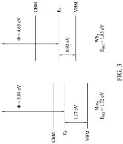
- The development of 2D crystal hetero-structures, specifically WS2/MoS2 hetero-structures, is achieved through chemical vapor deposition or sulfurization, enabling type-II band alignment and increased electron concentration by injecting electrons from WS2 to MoS2, thereby enhancing field-effect mobility and photoluminescence intensity.
Confined growth of 2d materials and their heterostructures
PatentWO2024049771A1
Innovation
- The development of layer-by-layer growth techniques for 2D materials on arbitrary substrates, using a SiO2 mask on amorphous Al2O3 or HfO2 layers to confine growth within trenches, allowing precise control of TMD layer formation and enabling single-domain homojunction and heterojunctions at a wafer scale.


Supply Chain Challenges for 2D Semiconductor Production
The commercialization of 2D semiconductor heterostructures faces significant supply chain challenges that currently impede widespread industrial adoption. The production of these advanced materials requires exceptionally pure precursors and substrates with atomically precise surfaces, creating bottlenecks in material sourcing. Current suppliers are predominantly small-scale specialty chemical companies and research institutions that lack the capacity for industrial-scale production.
Manufacturing processes for 2D semiconductors remain largely laboratory-based, with limited standardization across the industry. The transition from lab-scale production to industrial manufacturing faces substantial hurdles in maintaining quality consistency while scaling up volumes. Critical equipment for atomic layer deposition and chemical vapor deposition requires specialized modifications for 2D materials, yet few equipment manufacturers have developed commercially viable solutions optimized for these unique materials.
Quality control presents another major challenge, as conventional semiconductor metrology tools are often inadequate for characterizing atomically thin materials. The industry lacks standardized testing protocols and reference materials for 2D semiconductors, complicating supplier qualification and material certification processes. This absence of standards creates uncertainty in supply chain management and quality assurance.
Geographic concentration of expertise and production capabilities introduces additional vulnerabilities. Currently, research expertise is distributed across North America, Europe, and East Asia, but production capabilities for key materials and equipment are concentrated in specific regions, creating potential supply disruptions during geopolitical tensions or trade disputes.
Integration with existing semiconductor manufacturing infrastructure requires significant adaptation. The handling, processing, and integration of 2D materials differ substantially from conventional semiconductor materials, necessitating new protocols and equipment modifications throughout the supply chain. Many established semiconductor manufacturers lack the specialized knowledge and equipment needed to incorporate these novel materials into their production lines.
Intellectual property fragmentation further complicates supply chain development. Essential patents for 2D semiconductor production are held by various universities, research institutions, and companies across multiple jurisdictions. This dispersed IP landscape creates licensing complexities and potential legal barriers for companies attempting to establish comprehensive production capabilities.
To address these challenges, industry consortia and public-private partnerships are beginning to emerge, focusing on standardization, shared facilities, and coordinated research efforts. However, significant investment in supply chain development will be necessary before 2D semiconductor heterostructures can achieve commercial viability at scale.
Standardization Requirements for 2D Heterostructure Commercialization
The standardization of 2D semiconductor heterostructures represents a critical bottleneck in their commercial viability. Current manufacturing processes exhibit significant variations across research labs and production facilities, resulting in inconsistent material quality and device performance. To address this challenge, comprehensive standardization frameworks must be established across multiple dimensions of the production ecosystem.
Material characterization standards constitute the first essential requirement, encompassing uniform protocols for measuring key properties such as layer thickness, crystal quality, defect density, and interface characteristics. These standards should specify acceptable ranges for each parameter and detail the precise measurement techniques to be employed, enabling reliable comparison between materials produced by different manufacturers.
Fabrication process standardization presents another crucial dimension, requiring the development of industry-wide protocols for growth methods, transfer techniques, and post-processing treatments. This includes standardized parameters for chemical vapor deposition (CVD), molecular beam epitaxy (MBE), and mechanical exfoliation, as well as specifications for substrate preparation and environmental controls during production.
Device architecture standardization must address the geometric configurations, contact materials, and encapsulation techniques used in 2D heterostructure devices. This would facilitate interoperability between components from different manufacturers and streamline integration into existing semiconductor manufacturing lines.
Testing and qualification standards represent a fourth critical requirement, establishing uniform methodologies for evaluating electrical performance, thermal stability, and long-term reliability. These standards should define benchmark tests that accurately predict device behavior under various operating conditions and stress scenarios.
Metrology tool calibration standards are equally important, ensuring that measurement equipment used across the industry produces consistent and comparable results. This includes standardized calibration samples and procedures for tools such as atomic force microscopy, Raman spectroscopy, and electrical characterization equipment.
The development of these standardization frameworks requires collaborative efforts between academic institutions, industry players, and standards organizations. International bodies such as IEEE, SEMI, and ISO should coordinate working groups dedicated to 2D materials standardization, while government funding agencies could incentivize participation through targeted research programs. The establishment of open-access material databases and reference libraries would further accelerate the standardization process by providing benchmark materials against which new productions can be compared.
Unlock deeper insights with PatSnap Eureka Quick Research — get a full tech report to explore trends and direct your research. Try now!
Generate Your Research Report Instantly with AI Agent
Supercharge your innovation with PatSnap Eureka AI Agent Platform!