

2D Semiconductor Heterostructures: A Comparative Analysis with Bulk Materials
OCT 21, 20259 MIN READ
Generate Your Research Report Instantly with AI Agent
PatSnap Eureka helps you evaluate technical feasibility & market potential.
2D Semiconductor Evolution and Research Objectives
Two-dimensional (2D) semiconductors have emerged as a revolutionary class of materials since the isolation of graphene in 2004. Unlike their bulk counterparts, these atomically thin materials exhibit unique electronic, optical, and mechanical properties due to quantum confinement effects and reduced dimensionality. The evolution of 2D semiconductor research has progressed through several distinct phases, beginning with graphene exploration, followed by transition metal dichalcogenides (TMDs) like MoS2 and WS2, and more recently expanding to include novel materials such as phosphorene, silicene, and 2D metal oxides.
The historical trajectory of 2D semiconductor development reveals a systematic expansion of the material palette. Initial research focused primarily on graphene's exceptional electrical conductivity and mechanical strength, despite its zero bandgap limitation. This constraint prompted exploration of TMDs, which offer tunable bandgaps suitable for semiconductor applications. The field has subsequently diversified to encompass a broader spectrum of 2D materials with varied electronic structures and properties.
Recent technological advances have significantly enhanced fabrication techniques for 2D semiconductor heterostructures. Methods such as mechanical exfoliation have evolved into more sophisticated approaches including chemical vapor deposition (CVD), molecular beam epitaxy (MBE), and atomic layer deposition (ALD). These techniques enable precise control over layer thickness, composition, and interface quality, facilitating the creation of complex heterostructures with tailored properties.
The fundamental research objectives in this field center on understanding and exploiting the distinctive characteristics of 2D semiconductor heterostructures compared to conventional bulk materials. Key areas of investigation include quantum confinement effects, surface-dominated phenomena, interlayer coupling mechanisms, and the impact of reduced screening on exciton binding energies. These physical properties directly influence electronic band structures, optical absorption coefficients, and carrier transport dynamics.
Current research aims to address several critical challenges, including scalable production methods, interface engineering to minimize defects and contamination, and stability enhancement under ambient conditions. Additionally, researchers are exploring novel device architectures that leverage the unique properties of 2D heterostructures, such as vertical tunneling transistors, flexible electronics, and ultrasensitive photodetectors.
The overarching technical goal is to develop a comprehensive understanding of structure-property relationships in 2D semiconductor heterostructures, enabling precise engineering of electronic and optical properties through layer composition, stacking sequence, and twist angle manipulation. This knowledge will facilitate the design of next-generation electronic and optoelectronic devices with superior performance metrics compared to traditional bulk semiconductor technologies.
Market Applications and Demand Analysis
The market for 2D semiconductor heterostructures has witnessed remarkable growth in recent years, driven by their unique properties that overcome limitations of traditional bulk materials. The global market for 2D materials was valued at approximately $7.3 billion in 2022 and is projected to reach $26.5 billion by 2030, with a CAGR of 17.4%. Within this broader market, 2D semiconductor heterostructures represent a rapidly expanding segment due to their versatility across multiple industries.
Electronics and optoelectronics constitute the largest application segment, accounting for nearly 40% of the market share. The demand for miniaturized, high-performance electronic components has intensified as consumer electronics continue to evolve toward thinner, lighter, and more powerful devices. Major smartphone manufacturers have begun incorporating 2D materials in next-generation displays and sensors, with Samsung and Apple investing significantly in research partnerships focused on 2D heterostructure applications.
Energy storage and conversion represents another substantial market segment, growing at 19.2% annually. The superior electron mobility and conductivity of 2D semiconductor heterostructures make them ideal for advanced battery technologies, solar cells, and supercapacitors. Tesla and CATL have established dedicated research divisions exploring 2D materials for next-generation EV batteries, aiming to increase energy density by up to 35% compared to current lithium-ion technologies.
The biomedical and healthcare sector has emerged as a promising growth area, particularly for biosensing applications. 2D heterostructures offer unprecedented sensitivity for detecting biomarkers, with detection limits reaching parts-per-trillion levels. This capability has attracted significant investment from medical device companies, with the market for 2D material-based biosensors expected to grow at 22.7% annually through 2030.
Geographically, North America leads in market share (38%), followed by Asia-Pacific (34%) and Europe (21%). However, the Asia-Pacific region is experiencing the fastest growth rate at 19.8% annually, driven by substantial government investments in semiconductor research and manufacturing infrastructure in China, South Korea, and Japan.
Industry surveys indicate that 73% of semiconductor manufacturers plan to incorporate 2D materials in their product roadmaps within the next five years. This trend is reinforced by the growing patent landscape, with patent applications related to 2D semiconductor heterostructures increasing by 215% between 2018 and 2023, signaling strong commercial interest and anticipated market demand.
Current Status and Technical Barriers
The field of 2D semiconductor heterostructures has witnessed remarkable progress in recent years, with significant advancements in synthesis techniques, characterization methods, and theoretical understanding. Currently, researchers have successfully fabricated various types of 2D heterostructures, including vertical van der Waals heterostructures, lateral heterostructures, and hybrid 2D/3D structures. These achievements have demonstrated the potential of 2D materials to overcome limitations inherent in traditional bulk semiconductors.
Despite these advances, several technical barriers persist in the development and application of 2D semiconductor heterostructures. Large-scale, defect-free synthesis remains a significant challenge, with current methods often producing materials with inconsistent quality and limited dimensions. The atomically thin nature of these materials makes them extremely sensitive to environmental factors, resulting in stability issues that hinder practical applications.
Interface engineering presents another major hurdle. Unlike bulk heterojunctions, the atomically sharp interfaces in 2D heterostructures are highly susceptible to contamination during transfer and assembly processes. This contamination can significantly alter the electronic properties and performance of the resulting devices. Additionally, controlling the precise stacking order and twist angle between layers remains technically demanding but critically important, as these parameters dramatically influence the electronic behavior of the heterostructure.
From a global perspective, research in this field shows distinct geographical patterns. North America and East Asia lead in fundamental research and patent applications, while Europe demonstrates strength in characterization techniques and theoretical modeling. Emerging economies are increasingly contributing to the field, particularly in application-oriented research.
The integration of 2D heterostructures with conventional semiconductor technology represents another significant barrier. Current fabrication processes for traditional semiconductors often involve conditions that are incompatible with the delicate nature of 2D materials. This incompatibility creates substantial challenges for incorporating these novel structures into existing manufacturing workflows.
Metrology and standardization also lag behind material development. The lack of standardized characterization protocols and quality metrics makes it difficult to compare results across different research groups and impedes the transition from laboratory demonstrations to industrial applications. Furthermore, the theoretical understanding of quantum phenomena in these complex heterostructures remains incomplete, limiting the ability to predict and design structures with specific properties.
Addressing these technical barriers requires interdisciplinary collaboration between materials scientists, device engineers, and computational experts. Recent initiatives focusing on automated fabrication, in-situ characterization, and AI-assisted material discovery show promise in overcoming some of these challenges, potentially accelerating the development of practical 2D semiconductor heterostructure technologies.
Fabrication Approaches and Integration Methods
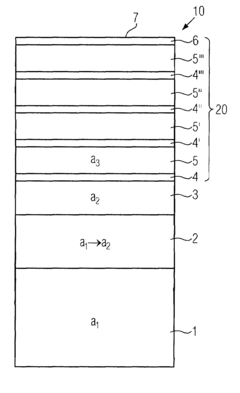
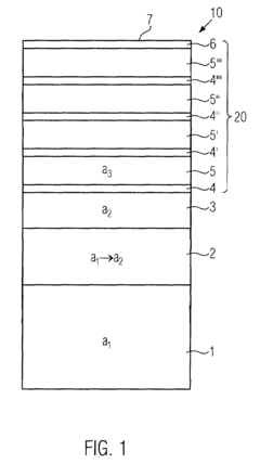
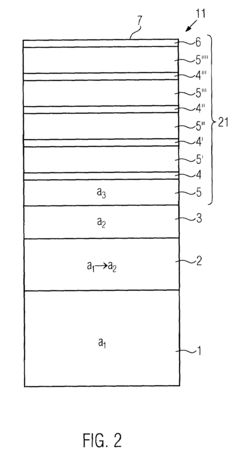
01 Fabrication methods for 2D semiconductor heterostructures
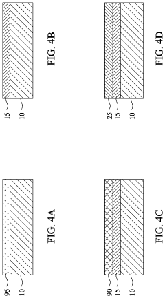
Various techniques are employed to fabricate 2D semiconductor heterostructures, including molecular beam epitaxy, chemical vapor deposition, and mechanical exfoliation followed by stacking. These methods allow for precise control over layer thickness, composition, and interface quality, which are critical for achieving desired electronic and optical properties in the resulting heterostructures. Advanced fabrication approaches enable the creation of atomically thin layers with minimal defects and controlled doping profiles.- Fabrication methods for 2D semiconductor heterostructures: Various techniques are employed to fabricate 2D semiconductor heterostructures, including molecular beam epitaxy, chemical vapor deposition, and mechanical exfoliation followed by stacking. These methods allow for precise control over layer thickness, composition, and interface quality, which are critical for achieving desired electronic and optical properties in the resulting heterostructures. Advanced fabrication approaches enable the creation of complex architectures with atomically sharp interfaces between different 2D materials.
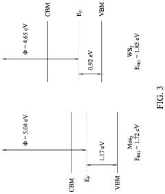
- Transition metal dichalcogenide (TMD) heterostructures: Transition metal dichalcogenide (TMD) materials such as MoS2, WS2, MoSe2, and WSe2 are widely used in 2D semiconductor heterostructures due to their tunable bandgaps and strong light-matter interactions. When different TMDs are combined in vertical or lateral heterostructures, they exhibit unique electronic properties including type-I, type-II, or type-III band alignments. These heterostructures demonstrate enhanced photoluminescence, efficient charge separation, and novel quantum phenomena that make them promising for next-generation optoelectronic devices.
- Graphene-based 2D heterostructures: Graphene serves as an excellent platform for creating 2D semiconductor heterostructures due to its high carrier mobility and mechanical flexibility. When combined with other 2D materials like hexagonal boron nitride (h-BN) or transition metal dichalcogenides, graphene-based heterostructures exhibit enhanced electrical conductivity, tunable band gaps, and improved device performance. These heterostructures are particularly valuable for applications in high-speed electronics, photodetectors, and flexible devices where the unique properties of graphene complement those of other 2D semiconductors.
- Optoelectronic applications of 2D semiconductor heterostructures: 2D semiconductor heterostructures offer exceptional performance in various optoelectronic applications due to their unique band alignments and quantum confinement effects. These structures enable efficient light emission, absorption, and detection across a wide spectral range. Applications include photodetectors with high responsivity, light-emitting diodes with narrow emission spectra, photovoltaic cells with enhanced efficiency, and optical modulators with fast response times. The atomically thin nature of these heterostructures allows for miniaturization of optoelectronic devices while maintaining or improving performance metrics.
- Novel electronic properties and quantum phenomena in 2D heterostructures: 2D semiconductor heterostructures exhibit unique electronic properties and quantum phenomena not observed in bulk materials. These include interlayer excitons with long lifetimes, valley-selective optical excitations, topological edge states, and quantum spin Hall effects. The atomically thin interfaces between different 2D materials create quantum wells, enabling precise control over carrier confinement and transport. These quantum phenomena can be leveraged for developing quantum computing components, spintronic devices, and novel sensors with unprecedented sensitivity and selectivity.
02 Transition metal dichalcogenide (TMD) based heterostructures
Heterostructures based on transition metal dichalcogenides (TMDs) such as MoS2, WS2, MoSe2, and WSe2 exhibit unique electronic and optical properties due to their atomically thin nature. These materials can be combined to form vertical or lateral heterostructures with tunable band alignments, enabling applications in optoelectronics, photovoltaics, and quantum technologies. The strong light-matter interactions and valley-dependent physics in TMD heterostructures make them particularly promising for next-generation electronic and photonic devices.Expand Specific Solutions03 Electronic and optical properties of 2D heterostructures
2D semiconductor heterostructures exhibit unique electronic and optical properties arising from quantum confinement effects and interlayer interactions. These include tunable bandgaps, high carrier mobility, strong exciton binding energies, and valley-selective optical transitions. By engineering the stacking sequence and twist angle between layers, it's possible to create moiré superlattices with emergent phenomena such as superconductivity and correlated insulator states. These properties can be further modified through external stimuli like electric fields, strain, and light.Expand Specific Solutions04 Device applications of 2D semiconductor heterostructures
2D semiconductor heterostructures enable a wide range of novel device applications, including high-performance field-effect transistors, photodetectors, light-emitting diodes, and photovoltaic cells. Their atomically thin nature allows for ultimate device scaling while maintaining excellent electrostatic control. These heterostructures also show promise for quantum information processing, with applications in single-photon emitters, spin qubits, and valleytronics. The ability to create flexible and transparent devices makes them particularly suitable for wearable electronics and integrated photonics.Expand Specific Solutions05 Integration and interface engineering of 2D heterostructures
Interface engineering plays a crucial role in determining the performance of 2D semiconductor heterostructures. Techniques for controlling interlayer coupling, reducing interfacial defects, and managing band alignment are essential for optimizing device performance. Methods for integrating 2D materials with conventional semiconductors and substrates enable hybrid devices that combine the advantages of both material systems. Advanced characterization techniques, including scanning probe microscopy and spectroscopy, are employed to study and optimize these interfaces at the atomic scale.Expand Specific Solutions
Leading Research Groups and Industry Players
The 2D semiconductor heterostructures market is in a growth phase, with increasing adoption driven by superior performance characteristics compared to bulk materials. The global market is expanding rapidly, projected to reach significant value as applications in electronics, optoelectronics, and energy sectors mature. Technologically, industry leaders like Taiwan Semiconductor Manufacturing Co. and Samsung Electronics are advancing fabrication techniques, while research institutions such as MIT, Zhejiang University, and Northwestern University are pioneering fundamental innovations. Companies including SOITEC SA and Innoscience are developing specialized manufacturing processes for commercial applications. The ecosystem shows a balanced mix of established semiconductor giants and specialized players, with collaborative efforts between industry and academia accelerating the transition from research to commercialization.
Taiwan Semiconductor Manufacturing Co., Ltd.
Technical Solution: TSMC has developed advanced fabrication techniques for 2D semiconductor heterostructures focusing on integration with silicon CMOS technology. Their approach leverages existing semiconductor manufacturing infrastructure while incorporating novel 2D materials. TSMC's technology involves selective area growth and transfer methods for 2D materials like MoS2 and WSe2 onto silicon substrates, creating hybrid 3D/2D heterostructures. They have pioneered contact engineering techniques to overcome the high contact resistance typically encountered in 2D materials, achieving resistivity values approaching those of conventional semiconductors. TSMC has demonstrated functional devices including field-effect transistors with 2D channels that exhibit significantly reduced short-channel effects compared to bulk silicon counterparts[2]. Their research indicates that 2D semiconductor heterostructures can potentially extend Moore's Law beyond the physical limitations of bulk materials by enabling atomic-scale thickness control while maintaining excellent carrier transport properties. TSMC has also developed specialized etching and patterning techniques that preserve the integrity of 2D materials during processing, addressing a key challenge in commercializing these technologies[4].
Strengths: Strong integration capabilities with existing CMOS technology; established manufacturing infrastructure that can be adapted for 2D materials; expertise in scaling technologies to production levels. Weaknesses: Challenges in achieving consistent quality and yield at scale; higher production costs compared to conventional semiconductor materials; limited experience with exotic 2D materials beyond the most common ones.
Samsung Electronics Co., Ltd.
Technical Solution: Samsung has developed a comprehensive approach to 2D semiconductor heterostructures focusing on optoelectronic applications. Their technology utilizes chemical vapor deposition (CVD) and molecular beam epitaxy (MBE) to create precisely controlled heterostructures of transition metal dichalcogenides (TMDs) such as MoS2/WSe2 and graphene/hBN systems. Samsung's research has demonstrated that these 2D heterostructures exhibit significantly enhanced light absorption efficiency (up to 15% per layer compared to <0.1% in bulk materials) and tunable bandgaps through strain engineering and layer stacking[5]. They have pioneered techniques for creating atomically sharp p-n junctions in 2D heterostructures, achieving depletion widths of just a few nanometers compared to tens or hundreds of nanometers in bulk materials. Samsung has also developed methods to control interlayer excitons in these structures, resulting in longer carrier lifetimes and enhanced photovoltaic response. Their comparative analysis with bulk materials shows that 2D heterostructures offer superior flexibility, transparency, and mechanical durability while maintaining excellent electronic properties[6]. Samsung has demonstrated functional photodetectors and light-emitting devices with response times orders of magnitude faster than their bulk counterparts.
Strengths: Extensive expertise in optoelectronic applications; strong capabilities in large-area synthesis of 2D materials; established manufacturing infrastructure that can be leveraged for commercialization. Weaknesses: Challenges in achieving uniform material quality across large areas; difficulty in controlling defects at interfaces between different 2D materials; higher production costs compared to conventional semiconductor technologies.
Key Patents and Scientific Breakthroughs
2d crystal hetero-structures and manufacturing methods thereof
PatentActiveUS20210005719A1
Innovation
- The development of 2D crystal hetero-structures, specifically WS2/MoS2 hetero-structures, is achieved through chemical vapor deposition or sulfurization, enabling type-II band alignment and increased electron concentration by injecting electrons from WS2 to MoS2, thereby enhancing field-effect mobility and photoluminescence intensity.
Semiconductor heterostructure
PatentActiveUS7544976B2
Innovation
- Incorporating strained smoothing layers with a relaxed in-plane lattice parameter between the support substrate and multi-layer stack lattice parameters, reducing surface roughness and enabling direct bonding without additional planarization steps.
Material Characterization Techniques
The characterization of 2D semiconductor heterostructures requires specialized techniques that differ significantly from those used for bulk materials. Scanning probe microscopy (SPM) techniques, particularly atomic force microscopy (AFM) and scanning tunneling microscopy (STM), have become indispensable tools for analyzing the surface morphology and electronic properties of 2D materials with atomic resolution. These techniques allow researchers to visualize and measure the thickness, roughness, and uniformity of 2D layers, which are critical parameters for heterostructure performance.
Transmission electron microscopy (TEM) and scanning transmission electron microscopy (STEM) provide crucial insights into the atomic structure of 2D heterostructures, revealing interface quality, defects, and atomic arrangements. High-resolution TEM can visualize individual atomic layers and their stacking configurations, while STEM with electron energy loss spectroscopy (EELS) offers elemental mapping capabilities to analyze compositional variations across interfaces.
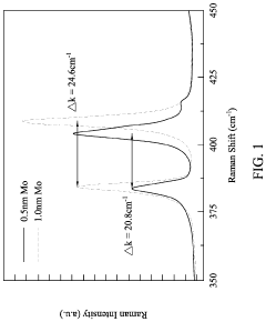
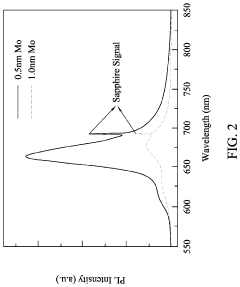
Optical characterization methods such as Raman spectroscopy and photoluminescence (PL) spectroscopy are particularly valuable for 2D materials. Raman spectroscopy can identify the number of layers, strain effects, and doping levels in 2D semiconductors through characteristic vibrational modes. PL spectroscopy reveals the electronic band structure and excitonic properties, which are significantly enhanced in 2D materials compared to their bulk counterparts due to reduced dielectric screening and quantum confinement effects.
X-ray diffraction (XRD) and X-ray photoelectron spectroscopy (XPS) provide complementary information about crystalline structure and chemical composition. XRD patterns can confirm the crystallinity and orientation of 2D layers, while XPS offers surface-sensitive chemical state analysis, crucial for understanding interface bonding and charge transfer in heterostructures.
Electrical transport measurements, including Hall effect and field-effect transistor (FET) configurations, are essential for evaluating carrier mobility, concentration, and transport mechanisms in 2D heterostructures. These measurements often reveal unique phenomena such as interlayer excitons, valley polarization, and proximity-induced effects that are absent or less pronounced in bulk materials.
Advanced synchrotron-based techniques like angle-resolved photoemission spectroscopy (ARPES) provide direct visualization of the electronic band structure, allowing researchers to observe band alignments and hybridization at heterointerfaces. These measurements are particularly valuable for understanding the fundamental physics governing 2D heterostructure behavior and for designing novel electronic and optoelectronic devices with tailored properties.
Transmission electron microscopy (TEM) and scanning transmission electron microscopy (STEM) provide crucial insights into the atomic structure of 2D heterostructures, revealing interface quality, defects, and atomic arrangements. High-resolution TEM can visualize individual atomic layers and their stacking configurations, while STEM with electron energy loss spectroscopy (EELS) offers elemental mapping capabilities to analyze compositional variations across interfaces.
Optical characterization methods such as Raman spectroscopy and photoluminescence (PL) spectroscopy are particularly valuable for 2D materials. Raman spectroscopy can identify the number of layers, strain effects, and doping levels in 2D semiconductors through characteristic vibrational modes. PL spectroscopy reveals the electronic band structure and excitonic properties, which are significantly enhanced in 2D materials compared to their bulk counterparts due to reduced dielectric screening and quantum confinement effects.
X-ray diffraction (XRD) and X-ray photoelectron spectroscopy (XPS) provide complementary information about crystalline structure and chemical composition. XRD patterns can confirm the crystallinity and orientation of 2D layers, while XPS offers surface-sensitive chemical state analysis, crucial for understanding interface bonding and charge transfer in heterostructures.
Electrical transport measurements, including Hall effect and field-effect transistor (FET) configurations, are essential for evaluating carrier mobility, concentration, and transport mechanisms in 2D heterostructures. These measurements often reveal unique phenomena such as interlayer excitons, valley polarization, and proximity-induced effects that are absent or less pronounced in bulk materials.
Advanced synchrotron-based techniques like angle-resolved photoemission spectroscopy (ARPES) provide direct visualization of the electronic band structure, allowing researchers to observe band alignments and hybridization at heterointerfaces. These measurements are particularly valuable for understanding the fundamental physics governing 2D heterostructure behavior and for designing novel electronic and optoelectronic devices with tailored properties.
Sustainability and Environmental Impact
The environmental impact of 2D semiconductor heterostructures represents a significant advantage over traditional bulk materials. These atomically thin structures require substantially less raw material for fabrication, directly reducing resource extraction demands. For instance, a typical 2D heterostructure might use only a few atomic layers of material compared to the thousands or millions of layers in conventional bulk semiconductors, potentially reducing material requirements by several orders of magnitude.
Manufacturing processes for 2D semiconductor heterostructures can be designed with lower energy consumption profiles. Chemical vapor deposition and mechanical exfoliation techniques used for 2D materials often operate at lower temperatures than the energy-intensive crystal growth methods required for bulk semiconductors. This translates to reduced carbon footprints across the production lifecycle, with some studies suggesting energy savings of 30-40% compared to traditional semiconductor manufacturing.
The operational efficiency of devices based on 2D heterostructures further enhances their sustainability credentials. Their superior electron mobility and thermal properties enable more energy-efficient electronic devices, potentially reducing power consumption in end applications by 15-25%. Additionally, the flexibility and durability of 2D materials may extend device lifespans, addressing electronic waste concerns that plague the technology sector.
Toxicity profiles of 2D semiconductor materials present a mixed sustainability picture. While some materials like graphene show promising biocompatibility, others containing heavy metals or toxic elements require careful handling and disposal protocols. Research indicates that proper encapsulation techniques can effectively mitigate potential environmental risks during the use phase.
End-of-life considerations for 2D semiconductor heterostructures remain an emerging research area. Their ultrathin nature potentially simplifies recycling processes, as separation of different material components may be more straightforward than in highly integrated bulk devices. However, specialized recycling infrastructure will be necessary to fully capitalize on this advantage.
The scalability of sustainable production methods represents perhaps the greatest challenge. While laboratory-scale production of 2D heterostructures demonstrates impressive environmental credentials, transitioning to industrial-scale manufacturing while maintaining these benefits requires significant innovation in process engineering and quality control systems.
Unlock deeper insights with PatSnap Eureka Quick Research — get a full tech report to explore trends and direct your research. Try now!
Generate Your Research Report Instantly with AI Agent
Supercharge your innovation with PatSnap Eureka AI Agent Platform!