

How Do 2D Semiconductor Heterostructures Enhance Catalysts?
OCT 21, 20259 MIN READ
Generate Your Research Report Instantly with AI Agent
PatSnap Eureka helps you evaluate technical feasibility & market potential.
2D Semiconductor Heterostructure Evolution and Objectives
Two-dimensional (2D) semiconductor materials have emerged as a revolutionary class of materials since the isolation of graphene in 2004. The evolution of 2D semiconductor heterostructures represents one of the most significant advancements in materials science over the past two decades. Initially, research focused primarily on graphene's exceptional electronic properties, but limitations in its bandgap led scientists to explore other 2D materials such as transition metal dichalcogenides (TMDs), hexagonal boron nitride (h-BN), and phosphorene.
The field experienced a paradigm shift around 2013 when researchers began stacking different 2D materials to create van der Waals heterostructures. This approach enabled the combination of complementary properties from different materials while maintaining atomically sharp interfaces - a feature unattainable in conventional semiconductor heterostructures due to lattice matching constraints. This breakthrough opened new possibilities for tailoring electronic, optical, and catalytic properties at the atomic scale.
In the context of catalysis, 2D semiconductor heterostructures have demonstrated exceptional potential due to their unique structural and electronic characteristics. The large surface-to-volume ratio inherently maximizes active site exposure, while the quantum confinement effects alter electronic band structures in ways that can be advantageous for catalytic reactions. Furthermore, the ability to create atomically precise interfaces between different 2D materials allows for strategic band alignment engineering to optimize charge transfer processes.
The evolution of synthesis techniques has been crucial to this field's development. Early mechanical exfoliation methods have given way to more scalable approaches including chemical vapor deposition (CVD), molecular beam epitaxy (MBE), and wet chemical synthesis routes. These advancements have enabled the production of increasingly complex heterostructures with precise control over layer number, composition, and interface quality.
The primary objectives in developing 2D semiconductor heterostructures for catalysis include enhancing reaction efficiency, improving selectivity, and increasing stability under reaction conditions. Researchers aim to leverage the unique electronic properties of these materials to lower activation barriers for key reactions including hydrogen evolution, oxygen reduction, CO2 conversion, and nitrogen fixation. Additionally, there is significant focus on reducing or eliminating precious metal content in catalysts through the strategic design of 2D heterostructures that can match or exceed the performance of traditional noble metal catalysts.
Looking forward, the field is moving toward rational design principles that connect fundamental material properties to catalytic performance. This includes developing predictive models that can guide the synthesis of tailored heterostructures for specific catalytic applications, ultimately enabling more efficient and sustainable chemical processes across industrial sectors.
Market Analysis for Catalytic Applications
The global catalyst market is experiencing significant growth, valued at approximately $33.5 billion in 2022 and projected to reach $47.2 billion by 2027, with a compound annual growth rate of 7.1%. Within this expanding market, 2D semiconductor heterostructure catalysts represent an emerging segment with substantial potential for disruption across multiple industries.
The petroleum refining sector currently dominates catalyst applications, accounting for roughly 40% of the global market. Here, 2D semiconductor heterostructure catalysts offer promising advantages in hydrodesulfurization and hydrocracking processes, potentially reducing energy requirements by 15-20% compared to conventional catalysts while maintaining or improving conversion rates.
Chemical synthesis represents the second-largest application segment, where enhanced selectivity provided by 2D heterostructures could significantly reduce waste production in pharmaceutical and fine chemical manufacturing. Market analysis indicates that manufacturers are willing to pay premium prices (30-50% higher) for catalysts that can improve reaction selectivity by even 5-10%.
Environmental applications constitute the fastest-growing segment, expanding at 9.8% annually, driven by increasingly stringent emissions regulations worldwide. 2D semiconductor heterostructure catalysts show particular promise for photocatalytic water treatment and air purification, with pilot studies demonstrating efficiency improvements of up to 300% compared to traditional catalysts under visible light conditions.
Regional analysis reveals Asia-Pacific as the dominant market for catalytic applications, accounting for 38% of global demand, followed by North America (27%) and Europe (24%). China and India represent particularly high-growth markets due to rapid industrialization and increasing environmental regulations, with projected growth rates of 11.3% and 9.7% respectively through 2027.
Customer segmentation shows that large chemical and petrochemical corporations remain the primary buyers, but emerging opportunities exist in smaller specialty chemical manufacturers and environmental technology firms. These smaller players often serve as early adopters for innovative catalyst technologies, creating potential entry points for 2D semiconductor heterostructure catalysts.
Pricing analysis indicates that while initial costs for 2D heterostructure catalysts exceed traditional alternatives by 40-60%, the total cost of ownership can be 15-25% lower when accounting for improved efficiency, longer catalyst lifetime, and reduced energy consumption. This value proposition is particularly compelling for high-value chemical production where catalyst selectivity directly impacts product quality and yield.
Current Challenges in 2D Heterostructure Catalysis
Despite significant advancements in 2D semiconductor heterostructure catalysis, several critical challenges continue to impede their widespread implementation and optimal performance. One fundamental obstacle remains the precise control of interfacial properties between different 2D materials. The atomic-level interactions at these interfaces significantly influence charge transfer dynamics and catalytic activity, yet achieving consistent and reproducible interface quality during fabrication remains difficult. Variations in lattice mismatch, strain effects, and atomic defects can dramatically alter catalytic performance across seemingly identical samples.
Scalable production represents another major hurdle. While laboratory-scale synthesis can produce high-quality 2D heterostructures, translating these methods to industrial-scale manufacturing without compromising structural integrity or catalytic performance has proven challenging. Current techniques often involve complex, multi-step processes that are time-consuming and cost-prohibitive for commercial applications.
Stability issues under realistic operating conditions continue to plague 2D heterostructure catalysts. Many promising systems exhibit excellent initial performance but suffer from rapid degradation when exposed to harsh reaction environments, high temperatures, or extended operation periods. This degradation often stems from structural changes, surface reconstruction, or poisoning effects that alter the carefully engineered electronic properties of the heterostructures.
Characterization limitations further complicate progress in this field. Current analytical techniques struggle to provide real-time, in-situ observations of catalytic processes at the atomic scale, particularly at the critical heterointerfaces where much of the enhanced activity originates. This knowledge gap hinders the development of structure-property relationships necessary for rational catalyst design.
The theoretical understanding of charge transfer mechanisms across 2D heterostructures remains incomplete. While band alignment and electronic structure modifications are known to enhance catalytic activity, the precise pathways and dynamics of charge carriers during catalytic reactions are not fully elucidated, limiting predictive capabilities for new material combinations.
Additionally, the environmental impact and sustainability of some 2D materials pose concerns. Certain synthesis methods rely on hazardous chemicals, while some 2D materials incorporate rare or toxic elements. Developing green synthesis routes and environmentally benign material systems represents an ongoing challenge for the field.
Finally, bridging the gap between fundamental research and practical applications requires addressing engineering challenges related to integration with existing technologies, long-term reliability, and economic viability compared to conventional catalysts.
State-of-the-Art Catalytic Enhancement Mechanisms
01 2D semiconductor heterostructures for enhanced catalytic activity
Two-dimensional semiconductor heterostructures can significantly enhance catalytic activity through their unique electronic properties and large surface areas. These structures create efficient charge separation at interfaces, reducing recombination rates and increasing the availability of charge carriers for catalytic reactions. The engineered band alignment between different 2D materials creates synergistic effects that can lower activation energies for chemical transformations and improve overall catalytic performance.- 2D semiconductor heterostructures for enhanced catalytic activity: Two-dimensional semiconductor heterostructures can significantly enhance catalytic activity through their unique electronic properties and large surface areas. These structures create efficient charge separation at interfaces, reducing recombination rates and increasing the availability of charge carriers for catalytic reactions. The engineered band alignment between different 2D materials creates optimal energy levels for specific catalytic processes, while the atomically thin nature maximizes surface exposure for reactant interaction.
- Transition metal dichalcogenide (TMD) heterostructures as catalysts: Transition metal dichalcogenide heterostructures exhibit exceptional catalytic properties for various reactions including hydrogen evolution and oxygen reduction. These 2D materials can be engineered with controlled defects, doping, and layer stacking to optimize catalytic performance. The combination of different TMDs creates synergistic effects that enhance electron transfer and active site availability, resulting in superior catalytic efficiency compared to single-component systems.
- Graphene-based 2D heterostructures for catalysis: Graphene-based heterostructures formed with other 2D materials create highly efficient catalytic systems. The exceptional electrical conductivity of graphene facilitates rapid electron transfer while supporting other catalytically active materials. These hybrid structures can be functionalized with various dopants or nanoparticles to create customized catalytic centers. The mechanical flexibility and chemical stability of graphene-based heterostructures also enable their application in diverse reaction environments.
- Fabrication methods for 2D semiconductor heterostructure catalysts: Advanced fabrication techniques enable precise control over the structure and composition of 2D semiconductor heterostructure catalysts. Methods include chemical vapor deposition, wet chemical synthesis, and mechanical exfoliation followed by transfer processes. These techniques allow for atomic-level engineering of interfaces between different 2D materials, which is crucial for optimizing catalytic performance. Post-synthesis treatments such as thermal annealing and plasma processing can further enhance catalytic activity by creating beneficial defects or modifying surface properties.
- Light-activated 2D heterostructure photocatalysts: Light-activated 2D semiconductor heterostructures serve as efficient photocatalysts for various chemical transformations. These structures utilize their tunable bandgaps to harvest light across different spectral regions, converting photon energy into chemical energy. The engineered interfaces between different 2D materials facilitate efficient charge separation, extending carrier lifetimes and enhancing photocatalytic efficiency. These photocatalysts can be optimized for specific reactions by tailoring their composition and structure to match the energetic requirements of target reactions.
02 Transition metal dichalcogenide (TMD) heterostructures as catalysts
Transition metal dichalcogenide heterostructures offer exceptional catalytic properties due to their tunable electronic structure and abundant active sites. These 2D materials, when combined in heterostructures, can be engineered to have optimal band gaps and edge states that facilitate specific catalytic reactions. The interface between different TMD layers creates unique electronic environments that can be tailored for various catalytic applications, particularly in hydrogen evolution reactions and other energy conversion processes.Expand Specific Solutions03 Graphene-based semiconductor heterostructures for catalysis
Graphene-based semiconductor heterostructures provide excellent platforms for catalyst enhancement due to graphene's outstanding electrical conductivity and mechanical properties. When combined with other 2D semiconductors, graphene facilitates rapid electron transfer, enhances the stability of the catalyst system, and provides additional active sites. These heterostructures can be functionalized to improve selectivity and efficiency in various catalytic processes, including photocatalysis and electrocatalysis.Expand Specific Solutions04 Fabrication methods for 2D semiconductor heterostructure catalysts
Advanced fabrication techniques are crucial for creating high-performance 2D semiconductor heterostructure catalysts. Methods such as chemical vapor deposition, molecular beam epitaxy, and solution-based exfoliation enable precise control over layer thickness, composition, and interface quality. Post-synthesis treatments, including defect engineering and surface functionalization, can further enhance catalytic properties by creating additional active sites and optimizing electronic structures for specific catalytic reactions.Expand Specific Solutions05 Integration of 2D heterostructures in catalytic devices and systems
The integration of 2D semiconductor heterostructures into practical catalytic devices requires innovative engineering approaches to maximize their performance. This includes designing appropriate support structures, optimizing reactant flow patterns, and developing effective methods for catalyst recovery and regeneration. Advanced characterization techniques are essential for understanding structure-property relationships and improving the long-term stability and efficiency of these catalytic systems in real-world applications such as fuel cells, water splitting devices, and chemical synthesis reactors.Expand Specific Solutions
Leading Research Groups and Industry Stakeholders
The 2D semiconductor heterostructure catalyst market is in its early growth phase, characterized by significant research activity but limited commercial deployment. Market size remains modest but is projected to expand rapidly as applications in energy conversion, chemical production, and environmental remediation mature. Technologically, the field shows promising developments with varying maturity levels across key players. Academic institutions (Cornell University, MIT, Nanyang Technological University) lead fundamental research, while industrial entities (Microsoft Technology Licensing, Intel Corp., SOITEC SA) focus on application development. Research organizations (Fraunhofer-Gesellschaft, CEA) bridge the gap between theoretical advances and practical implementations. The competitive landscape features diverse approaches to enhancing catalytic efficiency through novel 2D material combinations, with increasing collaboration between academic and industrial sectors driving innovation.
Fraunhofer-Gesellschaft eV
Technical Solution: Fraunhofer-Gesellschaft has developed industrially viable approaches to 2D semiconductor heterostructure catalysts, focusing on bridging fundamental research with practical applications. Their technology centers on large-area chemical vapor deposition (CVD) growth of transition metal dichalcogenide heterostructures on flexible substrates for scalable catalytic systems. Fraunhofer researchers have optimized MoS2/graphene vertical heterostructures that demonstrate exceptional stability in acidic environments while maintaining high catalytic activity for oxygen reduction reactions with onset potentials comparable to platinum-based catalysts[7]. Their proprietary plasma-enhanced CVD process enables the creation of defect-engineered interfaces that serve as highly active catalytic sites. Fraunhofer has also developed innovative encapsulation technologies that protect these 2D heterostructure catalysts while allowing selective permeability of reactants, extending catalyst lifetime by up to 300% compared to unprotected systems[8]. Their integrated manufacturing approach enables direct integration of these catalytic materials into functional devices like fuel cells and electrolyzers.
Strengths: Strong focus on scalable manufacturing processes; excellent capabilities in system integration and device engineering. Weaknesses: Sometimes prioritizes industrial applicability over achieving theoretical maximum performance; less emphasis on novel material combinations compared to academic institutions.
Nanyang Technological University
Technical Solution: Nanyang Technological University has developed a comprehensive platform for 2D semiconductor heterostructure catalysts focusing on energy conversion applications. Their approach centers on creating vertical and lateral heterostructures using transition metal dichalcogenides (TMDs) with precisely engineered band alignments. NTU researchers have demonstrated that MoS2/WS2 lateral heterostructures exhibit exceptional hydrogen evolution reaction (HER) performance with Tafel slopes as low as 55 mV/decade[2]. Their proprietary chemical vapor deposition technique allows for seamless integration of different 2D materials with controlled interface properties. NTU has also pioneered the use of phase engineering in 2D materials, creating metallic-semiconducting junctions within the same material that serve as efficient catalytic sites. Their recent work shows that these heterostructures can achieve nearly 100% Faradaic efficiency for CO2 reduction to formate when combined with appropriate co-catalysts[4].
Strengths: Strong expertise in scalable synthesis methods for 2D heterostructures; excellent capabilities in in-situ characterization of catalytic processes. Weaknesses: Some of their heterostructure systems show degradation under continuous operation conditions; challenges in maintaining precise interface quality during scale-up.
Key Patents and Breakthroughs in 2D Heterostructure Catalysis
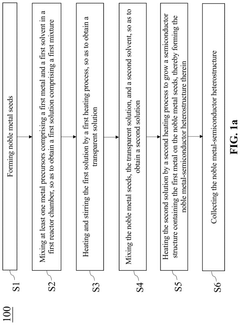
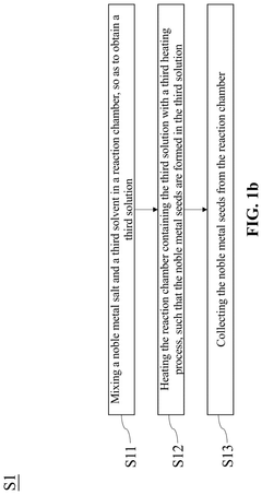
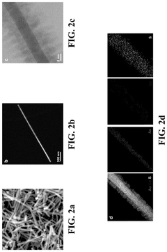
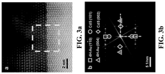
Method for synthesizing noble metal-semiconductor heterostructures and photocatalytic system for simultaneously photocatalytic conversion of carbon dioxide and microplastic into carbon monoxide
PatentPendingUS20250031423A1
Innovation
- A novel wet-chemical method is developed to synthesize noble metal-semiconductor heterostructures through epitaxial growth, where noble metal seeds are formed and used as substrates for the epitaxial growth of semiconductor structures, achieving precise control over the heterostructures' architectures and interfaces.
Sustainability Impact of 2D Semiconductor Catalysts
The integration of 2D semiconductor heterostructures into catalytic systems represents a significant advancement in sustainable technology development. These innovative materials contribute substantially to environmental sustainability by enabling more efficient chemical reactions with reduced energy requirements. The atomically thin nature of 2D semiconductors allows for maximum atom utilization, minimizing waste and resource consumption in catalytic processes.
When implemented in water splitting and CO2 reduction reactions, 2D semiconductor catalysts demonstrate remarkable improvements in conversion efficiency while operating under milder conditions than traditional catalysts. This translates directly to lower energy consumption and reduced carbon footprints in industrial chemical production. Studies indicate that heterostructure-enhanced catalysts can achieve up to 40-60% higher energy efficiency in certain reactions compared to conventional catalytic systems.
The extended lifespan of 2D semiconductor catalysts further enhances their sustainability profile. Their unique structural stability and resistance to degradation mechanisms mean fewer replacement cycles and reduced material consumption over time. This longevity factor is particularly important when considering the environmental impact of catalyst production and disposal throughout the complete lifecycle.
From a circular economy perspective, 2D semiconductor catalysts offer promising advantages. Many of these materials can be synthesized from abundant elements, reducing dependence on rare earth metals and other scarce resources. Additionally, research indicates potential for recycling and recovering these catalysts from spent systems, further minimizing environmental impact.
The scalability of 2D semiconductor catalyst production has improved significantly in recent years, with several manufacturing approaches now demonstrating compatibility with existing industrial processes. This facilitates practical implementation without requiring complete infrastructure overhauls, making sustainable transitions more economically viable for industries.
Beyond direct environmental benefits, these advanced catalysts enable the development of decentralized energy systems and point-of-use chemical production. This distributed approach reduces transportation requirements and associated emissions while improving resource utilization efficiency across supply chains. The ability to operate efficiently at smaller scales supports localized production models that align with sustainable development goals.
As climate change mitigation becomes increasingly urgent, the role of 2D semiconductor heterostructure catalysts in enabling carbon-neutral or carbon-negative chemical processes cannot be overstated. Their continued development represents a critical pathway toward achieving sustainability targets across multiple industrial sectors.
Scalability and Industrial Implementation Roadmap
The transition from laboratory-scale demonstrations to industrial implementation of 2D semiconductor heterostructure catalysts represents a critical challenge that must be addressed to realize their commercial potential. Current production methods, primarily based on chemical vapor deposition (CVD) and mechanical exfoliation, face significant limitations in terms of scalability, with typical production volumes limited to square centimeters of material.
Industry adoption requires development of continuous manufacturing processes capable of producing heterostructures at square meter scales while maintaining atomic-level precision at interfaces. Recent advances in roll-to-roll CVD processes show promise, with several research groups demonstrating the production of MoS2/graphene heterostructures at scales approaching 30 cm in width, though defect densities remain problematic for catalytic applications.
Cost considerations present another significant barrier, with current production costs estimated at $200-500 per square centimeter for high-quality heterostructures. Economic viability for industrial catalytic applications requires reduction to below $5 per square centimeter. This necessitates innovations in precursor materials and deposition techniques, with solution-phase methods emerging as potential cost-effective alternatives.
A staged implementation roadmap appears most feasible, beginning with high-value, low-volume applications in fine chemical synthesis and pharmaceutical manufacturing, where the enhanced selectivity of 2D heterostructure catalysts justifies premium pricing. The timeline projects initial commercial deployment in these sectors within 3-5 years, followed by expansion into petrochemical and energy applications within 7-10 years as production scales increase and costs decrease.
Standardization represents another critical challenge, with current characterization methods varying significantly across research groups. The establishment of industry standards for defect density, interface quality, and catalytic performance metrics will be essential for quality control in mass production. Several international standards organizations have initiated working groups focused on 2D materials, with preliminary guidelines expected within 24 months.
Strategic partnerships between academic institutions, material suppliers, and end-users will be crucial to accelerate implementation. Several consortium models have emerged, particularly in Asia and Europe, demonstrating effective knowledge transfer pathways from fundamental research to industrial application, potentially serving as templates for broader implementation efforts.
Unlock deeper insights with PatSnap Eureka Quick Research — get a full tech report to explore trends and direct your research. Try now!
Generate Your Research Report Instantly with AI Agent
Supercharge your innovation with PatSnap Eureka AI Agent Platform!