Investigation of Market Trends for 2D Semiconductor Heterostructures
OCT 21, 20259 MIN READ
Generate Your Research Report Instantly with AI Agent
Patsnap Eureka helps you evaluate technical feasibility & market potential.
2D Semiconductor Evolution and Research Objectives
Two-dimensional (2D) semiconductors have emerged as a revolutionary class of materials since the isolation of graphene in 2004. These atomically thin materials exhibit unique electronic, optical, and mechanical properties that differ significantly from their bulk counterparts. The evolution of 2D semiconductors has progressed from graphene to transition metal dichalcogenides (TMDs) such as MoS2 and WSe2, to more complex materials including hexagonal boron nitride (h-BN), phosphorene, and silicene.
The field has witnessed exponential growth in research publications, with annual papers increasing from fewer than 100 in 2010 to over 5,000 in 2022. This surge reflects both academic interest and industrial potential, particularly in next-generation electronics, optoelectronics, and quantum technologies. The technological trajectory suggests we are transitioning from fundamental research to application-oriented development, with heterostructures representing the frontier of innovation.
2D semiconductor heterostructures—created by stacking different 2D materials layer by layer—enable unprecedented control over electronic and optical properties through quantum confinement and interlayer interactions. These "van der Waals heterostructures" offer customizable band alignments, carrier mobilities, and optical responses that cannot be achieved with conventional semiconductor technologies.
Current research objectives in this field focus on several key areas. First, developing scalable and reproducible fabrication methods to overcome current limitations in production volume and consistency. Second, engineering heterostructures with precise control over twist angles and layer sequences to achieve specific electronic properties. Third, exploring novel material combinations beyond the well-studied graphene-TMD systems to expand the functional parameter space.
Additionally, researchers aim to enhance understanding of the fundamental physics governing interlayer interactions, particularly how these affect charge transfer, exciton formation, and quantum phenomena. This knowledge is essential for designing heterostructures with tailored properties for specific applications.
The ultimate technological goal is to develop commercially viable devices that leverage the unique advantages of 2D semiconductor heterostructures. These include ultra-thin, flexible electronics with superior performance metrics, highly efficient photodetectors and light emitters, and quantum devices operating at room temperature. Success in these objectives would position 2D semiconductor heterostructures as a transformative technology platform for the next generation of electronic and photonic systems.
Market Analysis for 2D Heterostructure Applications
The 2D semiconductor heterostructure market is experiencing robust growth, driven by the exceptional electronic, optical, and mechanical properties these materials offer. Current market valuations indicate the global 2D materials market reached approximately 7.5 billion USD in 2022 and is projected to grow at a compound annual growth rate (CAGR) of 19.2% through 2030. Within this broader market, heterostructures represent one of the fastest-growing segments due to their enhanced functionality compared to single-layer 2D materials.
Key application sectors demonstrating significant demand include electronics, where 2D heterostructures are revolutionizing transistor design with their atomically thin profiles and superior electron mobility. The optoelectronics sector shows particular promise, with market research indicating a potential 24% CAGR specifically for 2D heterostructure-based photodetectors and light-emitting devices through 2028.
Energy storage applications represent another high-growth segment, with 2D heterostructures being integrated into next-generation batteries and supercapacitors. Market analysis reveals that energy companies have increased R&D spending on 2D heterostructure technologies by 35% between 2020 and 2023, signaling strong commercial interest.
Geographically, North America currently leads market share at 38%, followed by Asia-Pacific at 34%, with China and South Korea making substantial investments in manufacturing infrastructure. European markets account for 22% of global demand, with particular focus on automotive and renewable energy applications.
Consumer electronics represents the largest end-user segment (41% of market share), followed by healthcare applications (23%) and industrial sensors (18%). The automotive sector, while currently accounting for only 12% of market demand, shows the highest projected growth rate at 27% annually through 2027.
Market barriers include high production costs, with current manufacturing expenses approximately 4-6 times higher than conventional semiconductor technologies. Scalability challenges persist, with 85% of commercial applications still utilizing small-area heterostructures under 10 cm².
Industry surveys indicate that 73% of semiconductor manufacturers plan to incorporate 2D heterostructures into their product roadmaps within the next five years. This trend is reinforced by patent analysis showing a 215% increase in 2D heterostructure-related patent filings between 2018 and 2023, with particular concentration in transistor, sensor, and energy storage applications.
The market demonstrates a clear shift from research-oriented demand toward commercial applications, with the ratio changing from 70:30 in 2018 to 45:55 in 2023, indicating increasing industrial adoption and commercialization momentum.
Global 2D Semiconductor Technology Landscape
The 2D semiconductor technology landscape has evolved dramatically since the isolation of graphene in 2004, which sparked a revolution in materials science. Currently, the global research and development ecosystem for 2D semiconductor heterostructures spans across North America, Europe, and Asia, with significant contributions from countries like the United States, China, South Korea, Japan, and several European nations. Each region demonstrates distinct research focuses and technological strengths in this emerging field.
The United States leads in fundamental research and early commercialization efforts, with major research institutions like MIT, Stanford, and national laboratories driving innovation. Silicon Valley startups have been particularly active in translating academic discoveries into viable products. Meanwhile, South Korea and Japan leverage their established semiconductor manufacturing expertise to advance 2D materials integration with existing technologies, with companies like Samsung and Sony making substantial investments.
China has rapidly expanded its research capabilities in this domain, emphasizing both fundamental science and applications development. The European Union, through initiatives like the Graphene Flagship program, has created collaborative networks that connect academic institutions with industry partners across multiple countries, fostering a coordinated approach to technology development.
Globally, research activities can be categorized into three main clusters: materials synthesis and characterization, device fabrication and testing, and systems integration. Materials synthesis research is particularly strong in the United States and China, while device engineering excellence is notable in South Korea, Japan, and Taiwan. Systems integration research is distributed more evenly across regions, with collaborative international projects becoming increasingly common.
Patent analysis reveals interesting geographical patterns, with the United States leading in fundamental technology patents, while Asian countries dominate in application-specific innovations. The technology transfer landscape shows varying models, from university spinoffs common in North America to large corporate R&D initiatives prevalent in East Asia.
Funding mechanisms also differ significantly across regions. In the United States, venture capital plays a crucial role alongside government grants, while in Asia, particularly China and South Korea, government-directed funding and large corporate investments dominate. The European approach tends to emphasize consortium-based funding through programs like Horizon Europe.
These regional differences create a complex but complementary global ecosystem, where technological advances in one region often catalyze developments elsewhere, driving the overall field forward through both competition and collaboration.
Current Fabrication Methods for 2D Heterostructures
01 Fabrication methods for 2D semiconductor heterostructures
Various techniques are employed to fabricate 2D semiconductor heterostructures, including molecular beam epitaxy, chemical vapor deposition, and mechanical exfoliation followed by stacking. These methods allow for precise control over the thickness and composition of each layer, enabling the creation of atomically thin heterostructures with tailored electronic properties. The fabrication processes often involve careful control of growth conditions to ensure high-quality interfaces between different 2D materials.- Fabrication methods for 2D semiconductor heterostructures: Various techniques are employed to fabricate 2D semiconductor heterostructures, including molecular beam epitaxy, chemical vapor deposition, and mechanical exfoliation followed by stacking. These methods allow for precise control over layer thickness, composition, and interface quality, which are critical for achieving desired electronic and optical properties in the resulting heterostructures. The fabrication processes often involve careful control of growth conditions such as temperature, pressure, and precursor flow rates to ensure high-quality interfaces between different 2D materials.
- Novel 2D materials for heterostructure applications: Research on 2D semiconductor heterostructures has expanded beyond graphene to include transition metal dichalcogenides (TMDs), hexagonal boron nitride (h-BN), phosphorene, and other emerging 2D materials. These materials offer diverse electronic properties ranging from semiconducting to insulating behaviors, enabling the creation of heterostructures with tailored band alignments and functionalities. The combination of different 2D materials allows for the engineering of quantum confinement effects, band offsets, and interfacial phenomena that can be exploited in next-generation electronic and optoelectronic devices.
- Electronic and optoelectronic applications of 2D heterostructures: 2D semiconductor heterostructures enable a wide range of electronic and optoelectronic applications, including field-effect transistors, photodetectors, light-emitting diodes, and solar cells. The atomically thin nature of these materials allows for efficient charge transport and light-matter interactions, while their van der Waals interfaces minimize issues related to lattice matching that plague conventional heterostructures. These properties make 2D heterostructures particularly promising for flexible, transparent, and ultra-compact electronic devices with enhanced performance characteristics.
- Quantum phenomena in 2D semiconductor heterostructures: 2D semiconductor heterostructures exhibit unique quantum phenomena due to their reduced dimensionality and interfacial effects. These include quantum confinement, valley polarization, exciton formation with high binding energies, and topological states. Researchers are exploring these quantum effects for applications in quantum computing, spintronics, and valleytronics. The ability to precisely control layer thickness and composition allows for engineering of quantum states and their interactions, opening new possibilities for quantum technologies.
- Integration of 2D heterostructures with conventional technologies: Integration of 2D semiconductor heterostructures with conventional semiconductor technologies and platforms represents a significant research direction. This includes developing methods for large-scale production, device fabrication processes compatible with existing manufacturing techniques, and hybrid systems combining 2D materials with silicon, III-V semiconductors, or photonic structures. Such integration efforts aim to leverage the unique properties of 2D materials while maintaining compatibility with established technological ecosystems, facilitating their adoption in commercial applications.
02 Transition metal dichalcogenide (TMD) heterostructures
Transition metal dichalcogenide (TMD) materials such as MoS2, WS2, MoSe2, and WSe2 are commonly used to form 2D semiconductor heterostructures. These materials exhibit unique electronic and optical properties when combined in vertical or lateral heterostructures. The band alignment between different TMD layers can be engineered to create type-I, type-II, or type-III heterostructures, enabling applications in optoelectronics, photovoltaics, and photodetectors. The atomically sharp interfaces between TMD layers facilitate efficient charge transfer and separation.Expand Specific Solutions03 Graphene-based 2D heterostructures
Graphene serves as an important component in many 2D semiconductor heterostructures, often functioning as a highly conductive electrode or as part of the active device region. When combined with other 2D materials like hexagonal boron nitride (h-BN) or TMDs, graphene-based heterostructures exhibit enhanced electrical, optical, and mechanical properties. These heterostructures can be designed with precise control over interlayer coupling and band alignment, enabling novel electronic devices with high carrier mobility and tunable bandgaps.Expand Specific Solutions04 Optoelectronic applications of 2D semiconductor heterostructures
2D semiconductor heterostructures are particularly promising for optoelectronic applications due to their strong light-matter interactions and tunable bandgaps. These heterostructures can be engineered to create efficient photodetectors, light-emitting diodes, photovoltaic cells, and optical modulators. The atomically thin nature of these materials allows for efficient charge separation at interfaces and reduced carrier transit times. Additionally, the direct bandgaps of many 2D semiconductors enable strong optical absorption and emission, making them ideal for next-generation optoelectronic devices.Expand Specific Solutions05 Quantum confinement effects in 2D heterostructures
Quantum confinement effects play a crucial role in determining the electronic and optical properties of 2D semiconductor heterostructures. When carriers are confined to atomically thin layers, their energy levels become quantized, leading to modified band structures and enhanced many-body interactions. These quantum effects can be exploited to create quantum wells, quantum dots, and other quantum-confined structures within 2D heterostructures. The resulting quantum confinement enables novel phenomena such as valley polarization, exciton condensation, and topological states, which can be harnessed for quantum information processing and spintronics applications.Expand Specific Solutions
Industry Leaders in 2D Semiconductor Research
The 2D semiconductor heterostructures market is currently in a growth phase, with increasing research activities and commercial applications emerging. The market size is expanding rapidly due to the unique electronic, optical, and mechanical properties these materials offer for next-generation electronics. Technologically, the field shows varying maturity levels across different applications. Leading players include Taiwan Semiconductor Manufacturing Co. (TSMC), which is integrating 2D materials into advanced semiconductor manufacturing; Massachusetts Institute of Technology (MIT) and Zhejiang University, which are pioneering fundamental research; and companies like Innoscience and Synopsys that are developing commercial applications. Intel and NaMLab are advancing integration with conventional semiconductor technologies, while universities such as National Taiwan University and University of Houston are exploring novel heterostructure combinations for specialized applications.
Taiwan Semiconductor Manufacturing Co., Ltd.
Technical Solution: TSMC has developed sophisticated 2D semiconductor heterostructure technologies focusing on integration with their advanced silicon manufacturing processes. Their approach combines traditional silicon CMOS with emerging 2D materials like graphene, hexagonal boron nitride (hBN), and transition metal dichalcogenides (TMDs) to create hybrid devices with enhanced performance characteristics[1]. TSMC has established specialized deposition techniques for creating uniform, large-area 2D material films compatible with their 300mm wafer processes, achieving thickness control at the atomic level. Their research demonstrates successful integration of 2D channel materials in field-effect transistors with high-k dielectrics, showing improved electrostatic control and reduced short-channel effects compared to conventional silicon devices[2]. TSMC has also developed proprietary contact engineering solutions to address the interface challenges between 2D materials and metals, significantly reducing contact resistance which has been a major bottleneck for 2D semiconductor commercialization[3].
Strengths: Unparalleled manufacturing infrastructure and process control capabilities; extensive experience in technology scaling and integration; strong position to commercialize 2D materials in high-volume applications. Weaknesses: Conservative approach to adopting radically new materials; challenges in maintaining yield when incorporating novel materials; significant investment required to adapt existing fabrication lines for 2D materials processing.
Massachusetts Institute of Technology
Technical Solution: MIT has pioneered groundbreaking research in 2D semiconductor heterostructures, focusing on novel stacking configurations of transition metal dichalcogenides (TMDs) and other 2D materials. Their approach involves precision assembly techniques using dry transfer methods with polymer stamps to create pristine interfaces between different 2D materials with atomic-level control[1]. MIT researchers have demonstrated moiré superlattices in twisted 2D heterostructures that exhibit exotic quantum phenomena including correlated insulator states and unconventional superconductivity[2]. Their work extends to developing scalable manufacturing processes for these materials, including controlled chemical vapor deposition (CVD) growth of lateral and vertical heterostructures with atomically sharp interfaces. MIT has also pioneered characterization techniques combining scanning tunneling microscopy, angle-resolved photoemission spectroscopy, and optical spectroscopy to map the electronic and optical properties of these novel heterostructures with unprecedented resolution[3].
Strengths: World-leading fundamental research capabilities; innovative fabrication techniques for creating pristine interfaces; strong interdisciplinary collaboration between physics, materials science, and engineering departments. Weaknesses: Focus primarily on fundamental science rather than commercial applications; fabrication methods often limited to laboratory scale; challenges in translating research discoveries into manufacturable technologies.
Key Patents and Scientific Breakthroughs
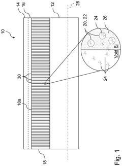
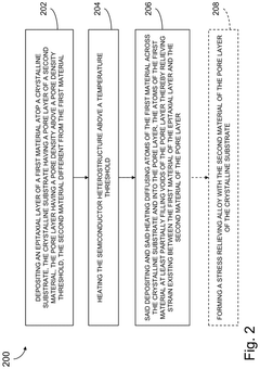
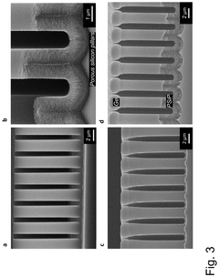
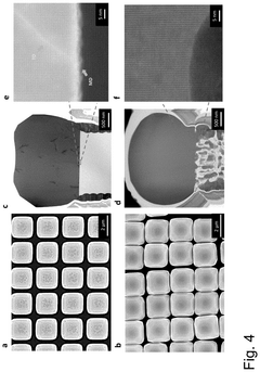
Semiconductor heterostructure and method of manufacturing same
PatentPendingUS20240332019A1
Innovation
- A method involving the deposition of an epitaxial layer on a crystalline substrate with a porous layer, where the porous layer's pore density is above a threshold, and subsequent heating to diffuse atoms and relieve strain, potentially forming a strain-relieving alloy, thereby reducing dislocation densities and improving surface quality.
Supply Chain Analysis for 2D Semiconductor Materials
The global supply chain for 2D semiconductor materials represents a complex ecosystem that has evolved significantly over the past decade. Currently, the production of high-quality 2D materials such as graphene, transition metal dichalcogenides (TMDs), and hexagonal boron nitride (h-BN) remains concentrated among specialized manufacturers in North America, Europe, and East Asia. These regions have established advanced fabrication capabilities that support the growing demand for heterostructure applications.
Raw material sourcing presents a notable challenge in the supply chain, with critical elements like molybdenum, tungsten, and high-purity carbon facing potential bottlenecks. Approximately 70% of these raw materials originate from a limited number of countries, creating vulnerability to geopolitical tensions and trade restrictions. This concentration of resources has prompted leading semiconductor companies to develop strategic partnerships with mining operations and material refiners to secure stable supply channels.
The manufacturing process for 2D materials involves multiple specialized steps, including chemical vapor deposition (CVD), mechanical exfoliation, and epitaxial growth techniques. These processes require highly specialized equipment from vendors primarily located in Japan, Germany, and the United States. The equipment segment represents approximately 35% of the total supply chain value, highlighting its critical importance in the ecosystem.
Quality control and standardization remain significant challenges within the supply chain. The absence of universally accepted quality metrics for 2D materials has led to inconsistencies in material properties between different suppliers. Industry consortia have begun addressing this issue through collaborative efforts to establish standardized characterization protocols and material specifications tailored specifically for heterostructure applications.
Distribution networks for 2D semiconductor materials have evolved from primarily research-oriented channels to more commercially viable pathways. Specialized material suppliers now offer customized solutions for specific heterostructure configurations, with lead times decreasing from months to weeks for standard material combinations. This improvement in logistics has accelerated product development cycles for end-users in electronics, photonics, and sensing applications.
Emerging regional hubs in Singapore, South Korea, and Taiwan are increasingly important in the 2D materials supply chain, offering integrated manufacturing capabilities that combine material production with device fabrication. These hubs benefit from strong government support through targeted funding initiatives and favorable regulatory frameworks designed to attract investment in advanced materials production infrastructure.
Sustainability Aspects of 2D Semiconductor Production
The sustainability of 2D semiconductor production has emerged as a critical consideration in the rapidly evolving landscape of advanced materials. As these novel heterostructures gain traction in commercial applications, their environmental footprint throughout the lifecycle demands thorough examination. Current production methods for 2D semiconductors, particularly those involving chemical vapor deposition (CVD) and mechanical exfoliation, present significant sustainability challenges due to high energy consumption and the use of hazardous precursors.
Energy intensity represents a primary concern, with CVD processes typically requiring temperatures exceeding 800°C maintained for extended periods. This translates to substantial energy demands that contribute to carbon emissions when powered by non-renewable sources. Additionally, the production of high-purity precursor materials involves energy-intensive refinement processes that compound the overall environmental impact.
Material efficiency in 2D semiconductor manufacturing remains suboptimal, with yield rates for high-quality heterostructures often below 30%. This inefficiency results in considerable material waste, particularly problematic given that many 2D materials incorporate rare elements with limited global reserves. The extraction of these elements frequently involves environmentally destructive mining practices that disturb ecosystems and contribute to habitat degradation.
Chemical usage presents another sustainability challenge. The synthesis of 2D semiconductor heterostructures typically requires solvents, etchants, and other chemicals that pose environmental and health risks. Many of these substances demonstrate high persistence in the environment and bioaccumulation potential, raising concerns about their long-term ecological impact. Furthermore, inadequate waste management practices in some production facilities exacerbate these issues.
Recent industry initiatives have begun addressing these sustainability concerns through several promising approaches. Innovations in low-temperature synthesis methods have demonstrated potential to reduce energy requirements by up to 40% compared to conventional techniques. Closed-loop production systems that recover and recycle precursor materials have shown capability to improve material utilization efficiency by 25-35% in pilot implementations.
Water consumption represents another critical sustainability factor, with traditional semiconductor manufacturing requiring substantial volumes for cleaning and processing. Emerging waterless and water-efficient techniques specifically designed for 2D material production could reduce water usage by up to 60% compared to conventional semiconductor manufacturing processes, though these approaches remain in early development stages.
As the industry matures, establishing comprehensive sustainability metrics and standardized lifecycle assessment methodologies specific to 2D semiconductor production will be essential for meaningful progress. The development of these frameworks, coupled with regulatory incentives for sustainable practices, will likely shape the evolution of production technologies and determine the environmental viability of 2D semiconductor heterostructures in future electronic applications.
Unlock deeper insights with Patsnap Eureka Quick Research — get a full tech report to explore trends and direct your research. Try now!
Generate Your Research Report Instantly with AI Agent
Supercharge your innovation with Patsnap Eureka AI Agent Platform!