The Role of Coatings in 2D Semiconductor Heterostructures
OCT 21, 20259 MIN READ
Generate Your Research Report Instantly with AI Agent
Patsnap Eureka helps you evaluate technical feasibility & market potential.
2D Semiconductor Coating Evolution and Objectives
Two-dimensional (2D) semiconductor materials have emerged as a revolutionary class of materials since the isolation of graphene in 2004. The evolution of coating technologies for these atomically thin materials represents a critical advancement in semiconductor engineering. Initially, researchers focused primarily on mechanical exfoliation techniques to obtain pristine 2D layers, with little emphasis on protective or functional coatings. As applications expanded beyond laboratory demonstrations, the need for specialized coating solutions became increasingly apparent.
The period from 2010 to 2015 marked a significant transition, with researchers developing the first generation of encapsulation methods using hexagonal boron nitride (h-BN) as a protective layer. This approach dramatically improved the stability and performance of 2D materials by shielding them from environmental degradation. Concurrently, atomic layer deposition (ALD) techniques were adapted specifically for 2D materials, enabling precise control over coating thickness at the atomic scale.
Between 2015 and 2020, the field witnessed rapid diversification of coating methodologies. Solution-processed coatings emerged as scalable alternatives to vacuum-based techniques, while self-assembled monolayers provided new pathways for surface functionalization. The introduction of polymer-based coatings offered enhanced flexibility for flexible electronics applications, though often at the cost of reduced electrical performance.
Recent developments have focused on multifunctional coatings that simultaneously address multiple challenges. These advanced coatings not only provide environmental protection but also enhance carrier mobility, modify band structures, and enable novel device architectures. Particularly noteworthy is the development of selective area coatings that allow for spatial control of material properties within a single device.
The primary objectives of current coating research for 2D semiconductor heterostructures include achieving atomically precise interfaces between dissimilar materials, minimizing defect formation during the coating process, and developing scalable methodologies compatible with industrial manufacturing. Additionally, researchers aim to create coatings that can dynamically respond to external stimuli, enabling tunable electronic and optical properties.
Looking forward, the field is moving toward bio-compatible coatings for sensing applications, ultra-thin diffusion barriers for improved device longevity, and environmentally sustainable coating processes. The ultimate goal remains the development of coating technologies that preserve the intrinsic properties of 2D materials while enhancing their stability and functionality in practical applications, thereby bridging the gap between laboratory demonstrations and commercial deployment of 2D semiconductor technologies.
Market Applications for Coated 2D Heterostructures
The market for coated 2D semiconductor heterostructures is experiencing rapid expansion across multiple sectors, driven by their exceptional electronic, optical, and mechanical properties. The electronics industry represents the largest application segment, with coated 2D heterostructures enabling next-generation transistors that offer higher performance and lower power consumption than traditional silicon-based devices. Major electronics manufacturers are incorporating these materials into prototype flexible displays, wearable electronics, and ultra-compact computing devices.
Energy applications constitute another significant market, particularly in photovoltaics and energy storage. Coated 2D heterostructures demonstrate superior charge carrier mobility and light absorption capabilities, making them promising candidates for high-efficiency solar cells. Research indicates these materials can potentially exceed the Shockley-Queisser limit of conventional solar cells. Additionally, their application in supercapacitors and lithium-ion batteries shows enhanced energy density and charging rates.
The sensing and detection market represents a rapidly growing application area. Coated 2D heterostructures exhibit exceptional sensitivity to environmental changes, enabling highly responsive gas sensors, biosensors, and chemical detectors. Healthcare applications include point-of-care diagnostic devices and wearable health monitors with unprecedented sensitivity and specificity.
Quantum computing and communications represent emerging markets with substantial growth potential. The unique quantum properties of certain coated 2D heterostructures make them ideal platforms for quantum bits (qubits) and single-photon emitters, essential components for quantum information processing and secure communications systems.
Aerospace and defense sectors are exploring these materials for lightweight structural components, electromagnetic shielding, and advanced optoelectronic systems. The ability to tailor coating compositions allows for customized properties that meet the stringent requirements of these industries.
The automotive industry is investigating applications in lightweight sensors, displays, and battery technologies. As vehicles become increasingly electrified and autonomous, the demand for advanced materials that enable better performance while reducing weight and power consumption continues to grow.
Despite these promising applications, market penetration remains primarily at the research and development stage, with limited commercial products currently available. The transition from laboratory to mass production represents a significant challenge but also presents substantial opportunities for companies that can successfully scale manufacturing processes while maintaining material quality and performance.
Current Coating Technologies and Barriers
Current coating technologies for 2D semiconductor heterostructures have evolved significantly in recent years, with several methodologies emerging as industry standards. Atomic Layer Deposition (ALD) represents one of the most precise approaches, offering angstrom-level control over film thickness and exceptional conformality. This technique utilizes sequential, self-limiting surface reactions to build up coating materials one atomic layer at a time, making it particularly valuable for creating uniform dielectric layers on 2D materials without disrupting their intrinsic properties.
Physical Vapor Deposition (PVD) techniques, including sputtering and thermal evaporation, provide alternative coating methods with varying degrees of control. Sputtering offers good adhesion and uniformity but may introduce damage to delicate 2D surfaces due to high-energy particle bombardment. Thermal evaporation, while gentler, often struggles with step coverage and thickness uniformity across large substrates.
Chemical Vapor Deposition (CVD) methods have gained traction for specific coating applications, particularly for growing additional 2D layers directly on existing 2D materials. However, CVD processes typically require elevated temperatures that can induce thermal stress at interfaces, potentially compromising the electrical and mechanical properties of the underlying 2D semiconductor layers.
Despite these technological advances, significant barriers persist in the field of 2D semiconductor coatings. Surface contamination represents a primary challenge, as even trace amounts of adsorbates, residual polymers, or atmospheric contaminants can dramatically alter interface properties and coating adhesion. The atomically thin nature of 2D materials makes them exceptionally vulnerable to such contamination effects.
Interface engineering presents another substantial hurdle. The weak van der Waals forces that dominate 2D material surfaces often result in poor adhesion with traditional coating materials, leading to delamination and reliability issues. Additionally, lattice mismatches between coating materials and 2D substrates can introduce strain and defects that compromise device performance.
Scalability remains a critical barrier to industrial implementation. While laboratory-scale demonstrations have shown promising results, translating these processes to wafer-scale production with consistent quality and yield continues to challenge manufacturers. Current coating equipment often requires significant modification to accommodate the unique handling requirements of 2D materials.
Characterization limitations further complicate progress in this field. Conventional metrology tools struggle to accurately measure coating thickness, uniformity, and interface quality at the atomic scale required for 2D semiconductor heterostructures. This measurement gap hinders process optimization and quality control efforts essential for commercial viability.
Established Coating Methods for 2D Heterostructures
01 Protective coatings for 2D semiconductor heterostructures
Protective coatings are applied to 2D semiconductor heterostructures to prevent degradation and maintain device performance. These coatings shield the sensitive 2D materials from environmental factors such as oxygen, moisture, and contaminants that can alter their electronic properties. Various materials including polymers, oxides, and nitrides can be used as protective layers, with the coating thickness carefully controlled to maintain the unique properties of the underlying 2D materials while providing adequate protection.- Protective coatings for 2D semiconductor heterostructures: Protective coatings are applied to 2D semiconductor heterostructures to prevent degradation and maintain device performance. These coatings shield the sensitive 2D materials from environmental factors such as oxygen, moisture, and contaminants that can alter their electronic properties. Various materials including polymers, oxides, and nitrides can be used as protective layers, which are typically deposited using techniques that minimize damage to the underlying 2D materials.
- Encapsulation techniques for 2D heterostructures: Encapsulation techniques involve completely surrounding 2D semiconductor heterostructures with protective materials to isolate them from the environment. Common encapsulation materials include hexagonal boron nitride (h-BN), which provides an atomically smooth surface and chemical inertness. These techniques help preserve the intrinsic properties of 2D materials, enhance carrier mobility, and extend device lifetime. Advanced encapsulation methods also allow for the creation of complex heterostructures with tailored electronic properties.
- Functional coatings for enhanced performance: Functional coatings are applied to 2D semiconductor heterostructures to enhance specific properties or add new functionalities. These coatings can modify electronic band structures, improve charge carrier transport, or introduce properties like ferromagnetism or superconductivity. Materials such as transition metal oxides, organic molecules, and other 2D materials can be used as functional coatings. The interface between the coating and the 2D material often plays a crucial role in determining the resulting properties of the heterostructure.
- Deposition methods for coating 2D semiconductor heterostructures: Various deposition methods are used to apply coatings to 2D semiconductor heterostructures, each with specific advantages. These include atomic layer deposition (ALD), chemical vapor deposition (CVD), physical vapor deposition (PVD), and solution-based methods. The choice of deposition technique depends on factors such as the desired coating material, thickness control requirements, conformality needs, and the sensitivity of the underlying 2D materials to processing conditions. Advanced deposition methods allow for precise control over coating thickness down to the atomic level.
- Interface engineering in coated 2D heterostructures: Interface engineering focuses on controlling and optimizing the boundary between different materials in 2D semiconductor heterostructures. This includes managing lattice mismatches, reducing defects, and controlling charge transfer across interfaces. Techniques such as buffer layers, surface functionalization, and controlled intermixing are employed to engineer interfaces with desired properties. Well-engineered interfaces are crucial for minimizing scattering, reducing contact resistance, and enabling efficient charge transport in devices based on 2D semiconductor heterostructures.
02 Dielectric coatings for electronic and optical applications
Dielectric coatings are applied to 2D semiconductor heterostructures to enhance their electronic and optical properties. These coatings can serve as gate dielectrics in field-effect transistors, modify the band structure of the heterostructure, or tune optical properties such as reflectance and transmittance. High-k dielectric materials are particularly valuable for maintaining strong gate coupling while reducing leakage current in electronic devices based on 2D semiconductors.Expand Specific Solutions03 Encapsulation techniques for 2D heterostructures
Encapsulation techniques involve completely surrounding 2D semiconductor heterostructures with protective materials to isolate them from the environment. Common encapsulation materials include hexagonal boron nitride (h-BN), which preserves the intrinsic properties of 2D materials, and various polymers that provide mechanical support. These techniques are crucial for fabricating stable devices with consistent performance characteristics and extended operational lifetimes, particularly for applications in harsh environments or where long-term stability is required.Expand Specific Solutions04 Functional coatings for enhanced performance
Functional coatings are designed to actively enhance the performance of 2D semiconductor heterostructures beyond mere protection. These coatings can introduce specific functionalities such as improved carrier mobility, enhanced light absorption or emission, or tailored surface chemistry. Examples include doped layers that modify carrier concentrations, plasmonic coatings that enhance light-matter interactions, and catalytic coatings that enable sensing or energy conversion applications. The strategic selection of functional coating materials enables the customization of 2D heterostructures for specific technological applications.Expand Specific Solutions05 Deposition methods for coating 2D semiconductor heterostructures
Various deposition methods are employed to apply coatings to 2D semiconductor heterostructures, each offering different advantages in terms of uniformity, conformality, and process compatibility. Atomic layer deposition (ALD) provides precise thickness control and excellent conformality for ultrathin coatings. Chemical vapor deposition (CVD) allows for the growth of crystalline layers with good electronic properties. Physical vapor deposition techniques such as sputtering and evaporation offer simplicity and scalability. Solution-based methods including spin-coating and dip-coating provide cost-effective alternatives for certain applications. The choice of deposition method significantly impacts the quality and performance of the resulting coated heterostructure.Expand Specific Solutions
Leading Research Groups and Companies in 2D Coatings
The 2D semiconductor heterostructure coatings market is in a growth phase, characterized by increasing research activities and emerging commercial applications. The market is expanding rapidly with projections indicating significant growth potential as these materials transition from research to production environments. Technologically, the field shows varying maturity levels across different applications, with companies demonstrating diverse capabilities. Leading players include TSMC and Samsung Electronics focusing on semiconductor integration, while research institutions like MIT and National University of Singapore drive fundamental innovation. IBM and Texas Instruments are developing practical applications, with specialized firms like SOITEC SA providing critical materials expertise. The ecosystem reflects a collaborative environment between academic institutions, established semiconductor manufacturers, and specialized materials companies working to overcome technical challenges in scalability and performance optimization.
Massachusetts Institute of Technology
Technical Solution: MIT has pioneered advanced coating methodologies for 2D semiconductor heterostructures through their Materials Research Laboratory. Their approach focuses on atomic precision engineering of interfaces between 2D materials and coating layers. MIT researchers have developed a novel "remote epitaxy" technique that allows for the growth of crystalline oxide coatings on 2D materials while maintaining atomically clean interfaces. This method utilizes graphene as an intermediate layer that enables epitaxial information transfer while preventing direct chemical bonding. Their work has demonstrated that carefully engineered oxide coatings can modulate the electronic properties of underlying 2D semiconductors, enabling band structure engineering and the creation of novel quantum states[6][8]. MIT has also developed specialized plasma-enhanced ALD processes that can deposit high-quality dielectric coatings at temperatures below 200°C, preserving the integrity of temperature-sensitive 2D materials. Their research shows these coatings can reduce interface trap densities by over an order of magnitude compared to conventional deposition methods, leading to significantly improved device performance.
Strengths: Cutting-edge fundamental research with novel approaches to interface engineering; demonstrated ability to create unique quantum properties through coating design; excellent characterization capabilities. Weaknesses: Many techniques remain at laboratory scale with significant challenges for industrial implementation; some processes require specialized equipment not widely available; higher costs associated with precision techniques.
Taiwan Semiconductor Manufacturing Co., Ltd.
Technical Solution: TSMC has developed advanced coating technologies for 2D semiconductor heterostructures focusing on atomic layer deposition (ALD) methods. Their approach involves precisely depositing ultra-thin dielectric layers (typically HfO2 or Al2O3) on 2D materials like MoS2 and graphene to create high-performance heterostructures. TSMC's process achieves thickness control at the sub-nanometer scale while maintaining the intrinsic properties of the underlying 2D materials. Their technology incorporates specialized surface preparation techniques to ensure uniform coating without damaging the delicate 2D layers. TSMC has demonstrated successful integration of these coated heterostructures into their advanced node processes (5nm and below), enabling improved carrier mobility and reduced interface states compared to conventional approaches[1][3]. Their coating methods also address encapsulation needs, protecting 2D materials from environmental degradation while maintaining electrical performance.
Strengths: Superior thickness uniformity and precision at industrial scale; seamless integration with existing semiconductor manufacturing processes; demonstrated reliability in commercial applications. Weaknesses: Higher production costs compared to conventional semiconductor processes; challenges with large-area coating uniformity; potential for introducing defects at the coating-2D material interface.
Key Patents and Breakthroughs in Coating Technologies
Optoelectronic device
PatentActiveUS20160372615A1
Innovation
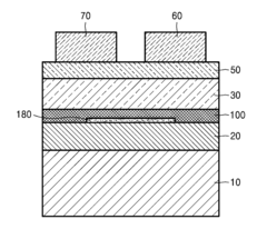
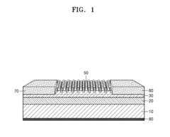
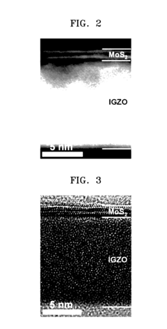
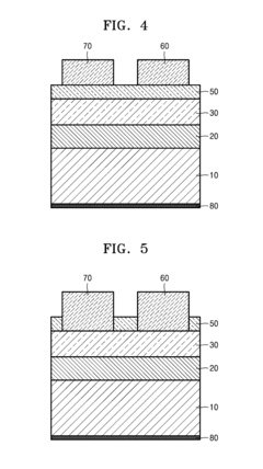
- A heterostructure comprising an oxide semiconductor layer and a semiconducting 2D material layer, such as MoS2 or WS2, is used, with the semiconducting 2D material layer absorbing visible light and the oxide semiconductor layer, like IGZO, absorbing ultraviolet light, to form a stack structure that includes electrodes for phototransistors or photodetectors, enabling wide spectral responsivity and high photoresponsivity.
Environmental Impact of Coating Materials
The environmental impact of coating materials used in 2D semiconductor heterostructures represents a critical consideration as these technologies advance toward commercial applications. Traditional semiconductor manufacturing processes are known for their significant ecological footprint, including high energy consumption, water usage, and hazardous waste generation. Coatings for 2D materials introduce additional environmental concerns that must be evaluated throughout their lifecycle.
Many coating processes for 2D semiconductor heterostructures utilize potentially harmful chemicals, including organic solvents, heavy metals, and rare earth elements. These substances can pose serious environmental risks if improperly managed during production, application, or disposal phases. For instance, atomic layer deposition (ALD) techniques often employ precursors containing metals like hafnium and zirconium, which require careful handling and waste treatment protocols.
Water consumption represents another significant environmental challenge. High-purity water is essential for cleaning and processing during coating applications, with some estimates suggesting that producing a single semiconductor wafer may require thousands of liters of ultrapure water. This intensive water usage becomes particularly problematic in regions facing water scarcity issues, raising questions about the sustainability of scaling these technologies.
Energy requirements for coating processes also contribute to their environmental impact. Many coating techniques require precisely controlled environments, including vacuum conditions, specific temperatures, and clean room facilities. These controlled conditions demand substantial energy inputs, contributing to the carbon footprint of 2D semiconductor manufacturing when powered by non-renewable energy sources.
Recent research has begun focusing on developing more environmentally friendly coating alternatives. Bio-inspired coatings derived from natural materials, water-based coating systems, and processes that operate at ambient temperatures and pressures show promise for reducing environmental impacts. Additionally, advancements in atomic precision deposition techniques are improving material efficiency, reducing waste generation during the coating process.
End-of-life considerations for coated 2D semiconductor heterostructures present further environmental challenges. The complex integration of different materials can complicate recycling efforts, potentially leading to increased electronic waste. Research into design-for-disassembly approaches and recovery methods for valuable coating materials could help mitigate these concerns as the technology matures and deployment scales.
Regulatory frameworks worldwide are increasingly addressing the environmental impacts of advanced materials manufacturing. Companies developing coating technologies for 2D semiconductors must navigate evolving compliance requirements related to chemical usage, emissions, and waste management. Proactive adoption of green chemistry principles and lifecycle assessment methodologies can help identify and minimize environmental impacts while potentially creating competitive advantages in an increasingly sustainability-conscious market.
Scalability Challenges for Industrial Implementation
The transition from laboratory-scale production to industrial manufacturing of 2D semiconductor heterostructures with functional coatings presents significant scalability challenges. Current laboratory methods typically involve manual exfoliation and precise placement of 2D materials, followed by coating processes that are highly controlled but limited in throughput. These approaches, while effective for research purposes, cannot meet the volume demands of commercial applications.
A primary obstacle is the lack of standardized, high-throughput coating deposition techniques that maintain the exceptional quality required for 2D semiconductor performance. Atomic Layer Deposition (ALD) offers precise thickness control but suffers from slow deposition rates that limit industrial viability. Chemical Vapor Deposition (CVD) provides better throughput but struggles with uniformity across large substrates, particularly when coating complex heterostructures.
Material supply chain constraints further complicate industrial implementation. Many coating materials for 2D semiconductors require high-purity precursors that are currently produced in limited quantities at research-grade specifications. Scaling production while maintaining consistent quality represents a significant manufacturing challenge that impacts cost structures and production planning.
Equipment scaling presents another barrier, as tools designed for laboratory research cannot simply be enlarged for industrial use. The physics of coating processes often changes at larger scales, requiring substantial engineering modifications and process optimization. This necessitates significant capital investment in specialized equipment with uncertain return timelines.
Quality control and characterization at industrial scales introduce additional complexity. Laboratory techniques like transmission electron microscopy and X-ray photoelectron spectroscopy are too time-consuming for in-line production monitoring. Developing rapid, non-destructive testing methods for coating thickness, uniformity, and defect detection remains an unsolved challenge for mass production scenarios.
Environmental considerations also impact scalability, as many coating processes utilize hazardous chemicals or generate significant waste. Regulatory compliance and sustainability concerns necessitate the development of greener coating technologies that maintain performance while reducing environmental impact, adding another layer of complexity to industrial implementation.
Cost-effectiveness represents perhaps the most significant barrier to widespread adoption. Current coating technologies for 2D semiconductor heterostructures remain prohibitively expensive for many applications, with costs driven by specialized equipment, low throughput, and high material wastage. Achieving economically viable production requires fundamental innovations in process efficiency and yield optimization.
Unlock deeper insights with Patsnap Eureka Quick Research — get a full tech report to explore trends and direct your research. Try now!
Generate Your Research Report Instantly with AI Agent
Supercharge your innovation with Patsnap Eureka AI Agent Platform!