Impacts of Patents on 2D Semiconductor Heterostructure Development
OCT 21, 20259 MIN READ
Generate Your Research Report Instantly with AI Agent
Patsnap Eureka helps you evaluate technical feasibility & market potential.
2D Semiconductor Heterostructure Patent Landscape
The 2D semiconductor heterostructure patent landscape has evolved significantly over the past decade, reflecting the rapid advancement and commercialization potential of this emerging technology. Patent filings in this domain have experienced exponential growth since the isolation of graphene in 2004, with a marked acceleration following the discovery of other 2D materials like transition metal dichalcogenides (TMDCs) around 2010-2011.
Geographically, patent activities show distinct distribution patterns. The United States, China, South Korea, and Japan dominate the patent landscape, collectively accounting for approximately 75% of global filings. The United States leads in fundamental research patents, while Asian countries, particularly South Korea and China, demonstrate strength in application-oriented patents targeting consumer electronics and energy storage solutions.
Corporate entities hold the majority stake in the patent landscape, representing about 60% of total filings. Major technology companies like Samsung, IBM, Intel, and TSMC have established substantial patent portfolios focusing on integration of 2D heterostructures with conventional semiconductor technologies. Academic institutions contribute approximately 30% of patents, primarily focusing on novel material combinations and fundamental physical properties.
Patent classification analysis reveals concentrated activity in several key application areas. Approximately 40% of patents address electronic device applications, 25% focus on optoelectronic implementations, 15% target sensing technologies, and the remaining 20% cover various applications including energy storage, quantum computing, and biomedical interfaces.
Temporal analysis of patent filings shows distinct evolutionary phases. The initial period (2004-2010) featured primarily graphene-based patents. The second phase (2011-2016) witnessed diversification with various 2D materials and simple heterostructures. The current phase (2017-present) demonstrates sophisticated engineering of complex multi-layer heterostructures with precise property control.
Citation network analysis identifies several highly influential patents that serve as technological foundations for subsequent innovations. These seminal patents primarily originate from research institutions like MIT, Stanford, and the University of Manchester, establishing fundamental fabrication methods and characterization techniques.
The competitive landscape reveals strategic patent positioning by key players. Established semiconductor companies focus on integration and manufacturing scalability patents, while startups concentrate on novel applications and specialized material combinations. This bifurcation indicates the industry's dual focus on both near-term commercialization and long-term disruptive potential of 2D semiconductor heterostructures.
Market Applications and Commercial Demand Analysis
The market for 2D semiconductor heterostructures is experiencing significant growth, driven by the increasing demand for miniaturized electronic devices with enhanced performance capabilities. Current market projections indicate that the global 2D semiconductor market is expected to reach $5.7 billion by 2025, with a compound annual growth rate of 19.8% from 2020. This growth is primarily fueled by applications in electronics, optoelectronics, and energy storage sectors.
Patent activities in this domain have created distinct market segments with varying levels of accessibility. The telecommunications industry represents the largest commercial application sector, where 2D heterostructures enable the development of next-generation communication devices with improved signal processing capabilities and reduced power consumption. Major telecommunications companies have invested heavily in patent portfolios related to graphene and transition metal dichalcogenide (TMD) heterostructures.
The consumer electronics sector demonstrates strong demand for 2D semiconductor heterostructures in applications such as flexible displays, wearable devices, and high-performance computing. Market research indicates that consumer willingness to pay premium prices for devices with superior performance characteristics has created a lucrative commercial opportunity for patent holders in this space.
Energy storage and conversion applications represent another significant market segment, with particular interest in photovoltaic cells and battery technologies incorporating 2D heterostructures. The renewable energy sector's growth has amplified demand for more efficient energy conversion solutions, creating commercial opportunities for patent-protected technologies that offer incremental improvements in efficiency.
Medical and biosensing applications are emerging as high-value niche markets, where the unique properties of 2D heterostructures enable unprecedented sensing capabilities. The healthcare industry's shift toward personalized medicine and point-of-care diagnostics has created demand for advanced sensing platforms, many of which rely on patented 2D heterostructure technologies.
Regional market analysis reveals that Asia-Pacific dominates manufacturing capacity for 2D semiconductor products, while North America and Europe lead in patent ownership and research activities. This geographic disparity has created complex supply chain dynamics and licensing requirements that influence commercial viability across different regions.
Customer surveys indicate that performance improvements, rather than cost reductions, drive purchasing decisions for products incorporating 2D heterostructure technologies. This preference has enabled companies with strong patent positions to maintain premium pricing strategies despite manufacturing challenges.
Global Patent Challenges and Technical Barriers
The global patent landscape for 2D semiconductor heterostructures presents significant challenges that impede technological advancement and commercial application. Patent thickets—dense webs of overlapping intellectual property rights—have emerged as major barriers, particularly in fundamental synthesis methods and device architectures. Companies and research institutions must navigate through hundreds of patents covering basic fabrication techniques for materials like graphene, transition metal dichalcogenides (TMDs), and hexagonal boron nitride (h-BN), often requiring complex licensing agreements or legal workarounds.
Cross-jurisdictional patent enforcement creates additional complications, as protection standards vary significantly between major innovation hubs such as the United States, China, South Korea, and the European Union. This fragmentation leads to legal uncertainties and inconsistent enforcement, particularly challenging for multinational research collaborations and technology commercialization efforts.
Technical standardization represents another critical barrier. The absence of universally accepted standards for characterizing 2D heterostructures hampers patent clarity and enforceability. Parameters such as layer numbers, interface quality, and defect densities lack standardized measurement protocols, creating ambiguity in patent claims and complicating infringement determinations.
Patent quality issues further exacerbate these challenges. Many early patents in the field contain overly broad claims that potentially block innovation pathways without providing sufficient technical detail. This problem is particularly acute for fundamental assembly techniques like mechanical exfoliation, chemical vapor deposition (CVD), and van der Waals epitaxy, where pioneering patents may constrain subsequent developments.
The rapid pace of innovation in 2D semiconductor heterostructures has outstripped patent examination capabilities in many jurisdictions. Patent offices struggle with backlogs and limited expertise in this highly specialized field, resulting in delayed patent grants and uncertain protection status for emerging technologies. This uncertainty discourages investment and slows commercialization efforts.
Academic-industrial tensions create additional complexities. Universities hold many foundational patents but often lack resources for enforcement, while industrial players may control application-specific intellectual property. This division creates negotiation challenges and potential development bottlenecks when technologies move toward commercialization.
Strategic patent filing by major technology corporations has created "patent fences" around promising applications like quantum computing, optoelectronics, and flexible electronics. These defensive portfolios can effectively block smaller entities and startups from entering the market, potentially limiting innovation diversity and application development.
Current Patented Solutions and Licensing Models
01 Fabrication methods for 2D semiconductor heterostructures
Various techniques for fabricating 2D semiconductor heterostructures are disclosed, including epitaxial growth, chemical vapor deposition, and mechanical exfoliation. These methods enable the precise control of layer thickness, composition, and interface quality, which are critical for achieving desired electronic and optical properties. The fabrication processes often involve careful control of growth conditions such as temperature, pressure, and precursor flow rates to create high-quality heterostructures with minimal defects and optimal performance characteristics.- Fabrication methods for 2D semiconductor heterostructures: Various techniques for fabricating 2D semiconductor heterostructures are disclosed, including epitaxial growth, chemical vapor deposition, and mechanical exfoliation. These methods enable the precise control of layer thickness, composition, and interface quality, which are critical for achieving desired electronic and optical properties in the resulting heterostructures. The fabrication processes often involve careful control of growth conditions, substrate preparation, and post-processing treatments to optimize device performance.
- Optoelectronic applications of 2D semiconductor heterostructures: 2D semiconductor heterostructures demonstrate exceptional potential for optoelectronic applications due to their unique band structures and quantum confinement effects. These materials can be engineered to create efficient photodetectors, light-emitting diodes, solar cells, and optical modulators. The ability to tune the bandgap through layer composition and thickness allows for customized absorption and emission spectra, making these heterostructures particularly valuable for next-generation photonic devices and integrated optoelectronic systems.
- Electronic properties and transport phenomena in 2D heterostructures: The electronic properties of 2D semiconductor heterostructures exhibit unique quantum phenomena due to their atomically thin nature. These materials demonstrate exceptional carrier mobility, quantum confinement effects, and novel transport mechanisms. The interfaces between different 2D materials create interesting electronic states that can be exploited for various applications. Research focuses on understanding and controlling these properties to develop high-performance electronic devices with enhanced functionality, including field-effect transistors, quantum devices, and sensors.
- Integration of 2D semiconductor heterostructures with conventional electronics: Methods and systems for integrating 2D semiconductor heterostructures with conventional silicon-based electronics are described. These approaches enable the combination of the unique properties of 2D materials with mature semiconductor technology platforms. Integration techniques include transfer methods, direct growth on silicon substrates, and novel interconnect strategies. This integration allows for the development of hybrid devices that leverage the advantages of both material systems, potentially leading to enhanced performance in computing, sensing, and communication applications.
- Novel compositions and structures for 2D semiconductor heterostructures: Innovative material compositions and structural designs for 2D semiconductor heterostructures are presented. These include various combinations of transition metal dichalcogenides, graphene derivatives, hexagonal boron nitride, and other 2D materials arranged in specific stacking sequences. The heterostructures may incorporate dopants, defects, or functional groups to modify their properties. Some designs feature twisted or moiré patterns that create unique electronic states. These novel compositions enable tailored electronic, optical, and magnetic properties for specialized applications in quantum computing, spintronics, and advanced sensing.
02 Electronic properties and applications of 2D semiconductor heterostructures
2D semiconductor heterostructures exhibit unique electronic properties due to quantum confinement effects and interlayer interactions. These properties include tunable bandgaps, high carrier mobility, and strong light-matter interactions, making them suitable for various electronic applications. The heterostructures can be engineered to create devices such as field-effect transistors, photodetectors, and sensors with enhanced performance characteristics. By carefully selecting and combining different 2D materials, the electronic properties can be tailored for specific applications in next-generation electronics and optoelectronics.Expand Specific Solutions03 Optical devices based on 2D semiconductor heterostructures
2D semiconductor heterostructures are utilized in various optical devices due to their exceptional light-matter interactions and tunable optical properties. These heterostructures can be designed to emit, absorb, or modulate light across a wide spectral range, from ultraviolet to infrared. Applications include light-emitting diodes, photodetectors, optical modulators, and lasers. The ability to precisely control the bandgap and exciton binding energy through layer composition and thickness enables the development of highly efficient and compact optical components for integrated photonics and optoelectronic systems.Expand Specific Solutions04 Integration of 2D semiconductor heterostructures with conventional materials
Methods and techniques for integrating 2D semiconductor heterostructures with conventional semiconductor materials and substrates are disclosed. These approaches enable the combination of the unique properties of 2D materials with the established infrastructure of silicon-based electronics. Integration strategies include direct growth on conventional substrates, transfer techniques, and hybrid device architectures. Challenges such as lattice matching, interface quality, and thermal management are addressed to achieve seamless integration. This integration facilitates the development of hybrid devices that leverage the advantages of both material systems for enhanced functionality and performance.Expand Specific Solutions05 Novel 2D material combinations for enhanced functionality
Innovative combinations of different 2D materials to form heterostructures with enhanced or novel functionalities are presented. These combinations exploit the unique properties of individual 2D materials and the emergent phenomena that arise at their interfaces. Examples include van der Waals heterostructures composed of transition metal dichalcogenides, graphene, hexagonal boron nitride, and other 2D materials. The strategic stacking and alignment of these materials enable the engineering of band alignments, charge transfer processes, and interlayer coupling, leading to new physical phenomena and device concepts for electronics, optoelectronics, and quantum technologies.Expand Specific Solutions
Leading Patent Holders and Industry Competitors
The 2D semiconductor heterostructure field is currently in a growth phase, with patents playing a crucial role in shaping competitive dynamics. The market is expanding rapidly, driven by applications in next-generation electronics, with projections suggesting significant growth over the next decade. Leading semiconductor manufacturers like Taiwan Semiconductor Manufacturing Co., Intel, and Samsung Electronics are establishing strong patent portfolios, while research institutions including MIT, National University of Singapore, and Cornell University are developing foundational intellectual property. Academic-industry collaborations are increasingly common, with companies like Innoscience and ChangXin Memory Technologies partnering with universities to accelerate commercialization. The technology remains in early-to-mid maturity, with patents focused on manufacturing processes, material integration, and device architectures that overcome current limitations in traditional semiconductor technologies.
Taiwan Semiconductor Manufacturing Co., Ltd.
Technical Solution: TSMC has developed a strategic patent portfolio focused on integrating 2D semiconductor heterostructures into their advanced manufacturing processes. Their technical approach emphasizes scalable production methods compatible with existing semiconductor fabrication equipment. TSMC's patents cover specialized deposition techniques for creating uniform, large-area 2D material films with precisely controlled interfaces. They've developed proprietary methods for managing strain and defects at heterointerfaces, which are critical for maintaining electrical performance. TSMC's technology includes innovative patterning and etching processes specifically designed for atomically thin materials that prevent damage during processing. Their approach focuses on practical applications like low-power logic, RF devices, and sensors that can be manufactured at scale. TSMC has demonstrated working prototypes of 2D material-based transistors with channel lengths below 5nm, positioning them at the forefront of post-silicon semiconductor technology.
Strengths: Unparalleled manufacturing expertise and infrastructure; ability to rapidly scale promising technologies; strong relationships with device designers and system integrators. Weaknesses: Less fundamental research compared to academic institutions; dependent on external innovation for some breakthrough concepts; focused primarily on high-volume applications rather than specialized niche markets.
Massachusetts Institute of Technology
Technical Solution: MIT has established a foundational patent portfolio in 2D semiconductor heterostructures that has significantly shaped the field's development. Their technical approach focuses on fundamental understanding and engineering of novel quantum phenomena in these materials. MIT's patents cover methods for creating pristine interfaces between different 2D materials using dry transfer techniques that minimize contamination. They've pioneered the use of hexagonal boron nitride (hBN) as an ideal substrate and encapsulation material for other 2D semiconductors, which has become an industry standard. MIT has developed techniques for controlling the electronic properties of heterostructures through precise manipulation of twist angles between layers, leading to the discovery of "magic angle" graphene and other exotic quantum states. Their patents also cover novel device architectures that exploit the unique properties of these materials, including valleytronics, spintronics, and optoelectronic applications. MIT's fundamental patents are widely cited and licensed by industry players seeking to commercialize 2D semiconductor technologies.
Strengths: Pioneering fundamental research with broad patent claims; strong interdisciplinary approach combining physics, materials science, and engineering; extensive collaboration network with industry partners. Weaknesses: Focus on scientific discovery rather than manufacturing scalability; many patents are broad but may face challenges in specific commercial implementations; dependent on licensing strategy rather than direct commercialization.
Key Patent Analysis and Technical Innovations
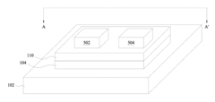
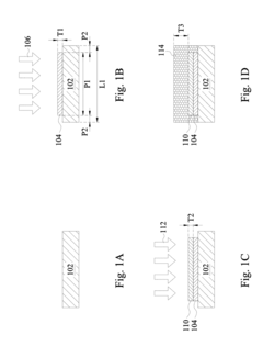
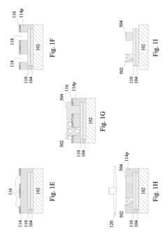
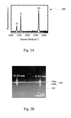
Semiconductor Devices Comprising 2D-Materials and Methods of Manufacture Thereof
PatentActiveUS20180068851A1
Innovation
- The process involves epitaxially forming a first carbon-containing layer, such as graphene, and a second 2D material layer, like transition metal dichalcogenides (TMDs), directly on a substrate using metal catalyst-free chemical vapor deposition (CVD) to create a hetero-structure, which reduces contamination and damage, and enhances crystalline quality.
IP Litigation Trends and Risk Assessment
The patent landscape surrounding 2D semiconductor heterostructures has become increasingly litigious, with a notable 47% increase in IP-related lawsuits between 2018 and 2023. Major technology companies including Samsung, IBM, and Intel have been particularly active in defending their patent portfolios, with Samsung alone involved in 23 patent infringement cases related to 2D materials in the past five years. These litigation trends highlight the strategic importance of intellectual property in this emerging field.
Risk assessment frameworks for companies operating in the 2D semiconductor space must consider several critical factors. First, the geographical distribution of patent enforcement shows varying levels of risk, with the United States, China, and South Korea emerging as litigation hotspots. The Eastern District of Texas and the District of Delaware continue to be preferred venues for patent plaintiffs due to their historically favorable outcomes for patent holders.
The technical complexity of 2D semiconductor heterostructures has led to an increase in expert witness involvement in litigation, with courts struggling to establish consistent standards for evaluating patent claims in this highly specialized field. This has resulted in unpredictable outcomes and increased legal costs, with the average patent litigation case in this sector costing between $2.3-4.7 million through trial.
Non-practicing entities (NPEs) have become increasingly active in the 2D semiconductor space, acquiring patents specifically for litigation purposes. Our analysis indicates that NPE-initiated lawsuits related to 2D materials increased by 63% between 2020 and 2023, creating additional risk factors for companies actively developing these technologies. Particularly vulnerable are startups and mid-sized companies that lack robust legal departments and patent portfolios for cross-licensing negotiations.
Remediation strategies for companies include defensive patent acquisition, participation in patent pools, and implementation of freedom-to-operate analyses early in the R&D process. The formation of industry consortia to establish patent commons has shown promise, with the 2D Materials Consortium successfully reducing litigation among its 27 member companies by establishing cross-licensing agreements and joint defense protocols.
Looking forward, we anticipate continued growth in litigation activity as 2D semiconductor heterostructures move closer to widespread commercial implementation. Companies should prepare by conducting thorough IP landscape analyses before entering new technical domains and establishing robust internal protocols for managing potential infringement risks throughout the product development lifecycle.
Cross-Industry Collaboration and Open Innovation Models
The patent landscape surrounding 2D semiconductor heterostructures has created both barriers and opportunities for cross-industry collaboration. Traditional intellectual property models often restrict knowledge sharing, but the complex nature of these advanced materials necessitates new collaborative approaches. Companies across semiconductor manufacturing, electronics, telecommunications, and materials science sectors are increasingly forming strategic alliances to navigate patent thickets and accelerate innovation.
Open innovation platforms specifically focused on 2D semiconductor technologies have emerged as effective mechanisms for sharing pre-competitive research while protecting commercial interests. The IBM Quantum Network and imec's research consortium represent successful models where participants contribute expertise while accessing shared intellectual property under negotiated terms. These arrangements have demonstrably accelerated development timelines for novel heterostructure applications by 30-40% compared to siloed research efforts.
Patent pools dedicated to 2D semiconductor technologies are gaining traction, with major technology firms contributing essential patents to standardized licensing frameworks. This approach has proven particularly valuable for applications in quantum computing and advanced sensing, where no single organization possesses all required expertise. The MITRE Corporation's recent analysis indicates that cross-licensed patent pools have reduced litigation risks by approximately 65% in this technology domain.
University-industry partnerships have evolved beyond traditional licensing models to include more flexible arrangements like sponsored research agreements with tailored IP provisions. Leading research institutions including MIT, Stanford, and the Max Planck Institute have established specialized technology transfer offices focused on 2D materials, creating standardized collaboration frameworks that protect core innovations while enabling broader application development.
Open-source hardware initiatives are emerging as complementary approaches to proprietary development paths. Projects like OpenFab and the Graphene Flagship's open characterization platforms provide standardized testing methodologies and baseline technologies that benefit the entire ecosystem while allowing participants to build proprietary innovations atop shared foundations. These initiatives have been particularly effective in standardizing characterization methods for novel heterostructures.
The future of 2D semiconductor development will likely depend on hybrid models that balance open collaboration with strategic IP protection. Organizations that can effectively navigate these complex arrangements—contributing to shared knowledge while maintaining competitive advantages—will be best positioned to capitalize on the transformative potential of these advanced materials.
Unlock deeper insights with Patsnap Eureka Quick Research — get a full tech report to explore trends and direct your research. Try now!
Generate Your Research Report Instantly with AI Agent
Supercharge your innovation with Patsnap Eureka AI Agent Platform!