Applications of 2D Semiconductor Heterostructures in Aerospace
OCT 21, 20259 MIN READ
Generate Your Research Report Instantly with AI Agent
Patsnap Eureka helps you evaluate technical feasibility & market potential.
2D Semiconductor Heterostructures Background and Objectives
Two-dimensional (2D) semiconductor heterostructures represent one of the most promising frontiers in materials science since the isolation of graphene in 2004. These atomically thin materials, consisting of layers with strong in-plane bonds and weak van der Waals interactions between layers, have revolutionized our understanding of condensed matter physics and opened new possibilities for next-generation electronics. The evolution of this technology has progressed from single-layer graphene to a diverse family of 2D materials including transition metal dichalcogenides (TMDs), hexagonal boron nitride (h-BN), phosphorene, and various 2D oxides.
The aerospace industry presents unique operational challenges including extreme temperature fluctuations, radiation exposure, weight constraints, and reliability requirements that conventional semiconductor technologies struggle to address effectively. 2D semiconductor heterostructures offer potential solutions to these challenges due to their exceptional mechanical flexibility, thermal stability, radiation hardness, and unprecedented strength-to-weight ratio.
The primary technical objectives for implementing 2D semiconductor heterostructures in aerospace applications include developing radiation-hardened electronics that can withstand the harsh space environment without performance degradation. Additionally, creating ultra-lightweight, flexible solar cells with high power conversion efficiency could revolutionize spacecraft power systems. Thermal management solutions leveraging the anisotropic thermal properties of these materials represent another critical objective.
Sensor technologies based on 2D materials offer unprecedented sensitivity for environmental monitoring, structural health assessment, and navigation systems. The development of high-frequency communication devices utilizing the unique electronic properties of these heterostructures could enable more efficient and reliable space communications. Furthermore, energy storage solutions with higher energy density and faster charging capabilities would address critical power management challenges in aerospace systems.
The historical trajectory of 2D materials research has seen exponential growth in publications and patents over the past decade, with significant milestones including the demonstration of vertical heterostructures in 2010, the development of large-area synthesis techniques around 2015, and recent breakthroughs in wafer-scale production methods. The technology is now transitioning from laboratory curiosities to engineered systems with practical applications.
Current research trends indicate accelerating progress in controlled synthesis, interface engineering, and device integration. The convergence of 2D semiconductor technology with advances in nanofabrication, quantum computing, and artificial intelligence is expected to further accelerate development and implementation in aerospace systems, potentially enabling transformative capabilities in space exploration, satellite technology, and aircraft performance.
Aerospace Market Demand Analysis
The aerospace industry is experiencing a significant shift towards advanced materials and technologies that can enhance performance while reducing weight and power consumption. 2D semiconductor heterostructures represent a revolutionary class of materials that align perfectly with these requirements. Current market analysis indicates the global aerospace electronics market is valued at approximately $6.8 billion, with projections showing growth to reach $9.3 billion by 2028, representing a compound annual growth rate of 6.7%.
The demand for 2D semiconductor heterostructures in aerospace applications is primarily driven by the need for radiation-hardened electronics that can withstand the harsh conditions of space. Traditional silicon-based semiconductors suffer from performance degradation when exposed to cosmic radiation, whereas certain 2D materials like MoS2 and WSe2 demonstrate superior radiation tolerance, making them ideal candidates for satellite electronics and deep space missions.
Weight reduction remains a critical factor in aerospace design, with each kilogram saved in satellite construction translating to approximately $20,000 in launch cost savings. The ultra-thin nature of 2D semiconductor heterostructures offers significant weight advantages over conventional electronics, potentially reducing the weight of electronic components by up to 70% while maintaining or improving performance metrics.
The growing commercial space sector, particularly the small satellite market which is expected to reach $13.7 billion by 2030, represents a substantial opportunity for 2D semiconductor applications. These materials enable the development of miniaturized yet powerful sensors, communication systems, and computing hardware essential for the next generation of CubeSats and nanosatellites.
Defense aerospace applications constitute another significant market segment, with military aircraft and UAVs requiring increasingly sophisticated electronic systems that can operate reliably in extreme conditions. The thermal stability and mechanical flexibility of 2D semiconductor heterostructures make them particularly valuable for avionics systems in high-performance military aircraft.
Energy efficiency demands in aerospace are also driving interest in these materials. With power generation being limited in space environments, the lower power consumption of 2D semiconductor-based electronics (potentially 40-60% less than silicon equivalents) represents a critical advantage for extended mission durations and expanded operational capabilities.
Market research indicates that aerospace companies are increasingly allocating R&D budgets toward next-generation materials, with major players like Boeing, Airbus, and Lockheed Martin establishing dedicated research divisions focused on 2D materials integration. This institutional investment signals strong industry confidence in the transformative potential of these technologies for future aerospace applications.
Current Status and Technical Challenges
The global landscape of 2D semiconductor heterostructures for aerospace applications has witnessed remarkable progress in recent years. Currently, these materials are transitioning from laboratory research to early-stage practical implementations in aerospace systems. Leading research institutions in the United States, China, Europe, and Japan have established dedicated programs focusing on 2D materials for extreme environments, with aerospace applications receiving particular attention due to their potential for weight reduction and performance enhancement.
The current technological readiness level (TRL) of 2D semiconductor heterostructures in aerospace applications varies significantly across different use cases. Sensing applications have reached TRL 4-5, with prototype demonstrations in relevant environments. However, more complex applications such as radiation-hardened electronics and thermal management systems remain at TRL 2-3, still requiring substantial development before field deployment.
Despite promising advances, several critical technical challenges impede widespread adoption. Material stability represents a primary concern, as 2D heterostructures must maintain their exceptional properties under extreme aerospace conditions including temperature fluctuations (-150°C to +150°C), vacuum exposure, and high radiation environments. Current encapsulation techniques provide inadequate protection against atomic oxygen erosion and cosmic radiation.
Scalable manufacturing presents another significant hurdle. Laboratory-scale production methods like mechanical exfoliation yield high-quality materials but are impractical for aerospace-grade components requiring consistency and reliability. Chemical vapor deposition (CVD) shows promise for larger-scale production but struggles with interface quality control and defect management when creating complex heterostructures.
Integration challenges with conventional aerospace systems persist, particularly regarding electrical contacts and interfaces. The atomically thin nature of these materials creates unique difficulties in establishing reliable connections with traditional aerospace electronics without degrading performance. Current bonding techniques often introduce defects or contamination at critical interfaces.
Reliability verification represents a substantial obstacle, as aerospace applications demand exceptional durability and predictable performance. The long-term behavior of 2D semiconductor heterostructures under cyclic loading, thermal cycling, and radiation exposure remains insufficiently characterized. Accelerated testing protocols specifically designed for these novel materials are still under development.
Standardization efforts are notably lacking, with no universally accepted characterization methods or quality metrics for aerospace-grade 2D heterostructures. This absence of standards complicates qualification processes and slows industry adoption. Several international working groups have recently formed to address this gap, but consensus standards remain years away from implementation.
Current Technical Solutions for Aerospace Applications
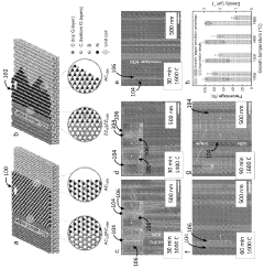
01 Fabrication methods for 2D semiconductor heterostructures
Various techniques are employed to fabricate 2D semiconductor heterostructures, including molecular beam epitaxy, chemical vapor deposition, and mechanical exfoliation followed by stacking. These methods allow for precise control over layer thickness, composition, and interface quality, which are crucial for achieving desired electronic and optical properties in the resulting heterostructures. The fabrication processes often involve careful control of growth conditions such as temperature, pressure, and precursor flow rates to ensure high-quality interfaces between different 2D materials.- Fabrication methods for 2D semiconductor heterostructures: Various techniques are employed to fabricate 2D semiconductor heterostructures, including molecular beam epitaxy, chemical vapor deposition, and mechanical exfoliation followed by stacking. These methods enable precise control over layer thickness, composition, and interface quality, which are crucial for achieving desired electronic and optical properties in the resulting heterostructures. Advanced fabrication approaches allow for the creation of atomically thin layers with minimal defects and controlled doping profiles.
- Transition metal dichalcogenide (TMD) based heterostructures: Heterostructures based on transition metal dichalcogenides (TMDs) such as MoS2, WS2, MoSe2, and WSe2 exhibit unique electronic and optical properties due to their atomically thin nature. These materials can be combined to form various types of heterojunctions including vertical, lateral, and mixed dimensional structures. TMD heterostructures demonstrate tunable bandgaps, strong light-matter interactions, and valley-dependent properties, making them promising for next-generation electronic and optoelectronic applications.
- Optoelectronic applications of 2D semiconductor heterostructures: 2D semiconductor heterostructures offer exceptional capabilities for optoelectronic devices due to their unique band alignments and quantum confinement effects. These structures enable efficient photodetectors, light-emitting diodes, photovoltaic cells, and optical modulators with enhanced performance characteristics. The ability to engineer band offsets and exciton binding energies in these heterostructures allows for tailored light absorption and emission properties, while their atomically thin nature facilitates integration with conventional photonic platforms.
- Electronic transport properties and device applications: The electronic transport properties of 2D semiconductor heterostructures can be engineered by controlling layer composition, stacking sequence, and interlayer coupling. These structures exhibit phenomena such as interlayer excitons, moiré superlattice effects, and topological states that can be exploited for novel electronic devices. Applications include high-mobility transistors, tunneling devices, memristors, and quantum computing components that leverage the unique quantum confinement and interfacial effects present in these atomically thin systems.
- Integration with other materials and computational modeling: 2D semiconductor heterostructures can be integrated with conventional semiconductors, metals, and dielectric materials to create hybrid systems with enhanced functionality. Computational modeling techniques, including density functional theory and machine learning approaches, are essential for predicting and optimizing the properties of these complex heterostructures. These modeling methods help in understanding interfacial phenomena, electronic band structures, and optical responses, accelerating the development of novel 2D heterostructure-based technologies.
02 Transition metal dichalcogenide-based heterostructures
Heterostructures based on transition metal dichalcogenides (TMDs) such as MoS2, WS2, MoSe2, and WSe2 exhibit unique electronic and optical properties due to their atomically thin nature. These materials can be combined to form various types of heterostructures including vertical stacks and lateral junctions. The band alignment between different TMD layers can be engineered to create type-I, type-II, or type-III heterojunctions, enabling applications in optoelectronics, photovoltaics, and quantum information processing. The strong light-matter interactions in these materials make them particularly promising for next-generation optoelectronic devices.Expand Specific Solutions03 Graphene-based 2D heterostructures
Graphene can be integrated with other 2D materials to form heterostructures with enhanced functionality. When combined with semiconducting 2D materials, graphene often serves as a highly conductive electrode or channel material. These heterostructures leverage graphene's exceptional electrical conductivity and mechanical strength while compensating for its lack of bandgap through integration with semiconducting 2D materials. Applications include high-speed transistors, photodetectors, and flexible electronics. The atomically smooth nature of graphene enables clean interfaces in these heterostructures, minimizing carrier scattering and improving device performance.Expand Specific Solutions04 Optoelectronic applications of 2D semiconductor heterostructures
2D semiconductor heterostructures exhibit exceptional optoelectronic properties that can be harnessed for various applications including photodetectors, light-emitting diodes, solar cells, and optical modulators. The atomically thin nature of these materials allows for efficient light absorption and emission, while their band structure can be engineered through layer stacking to optimize performance for specific wavelengths. The direct bandgap nature of many 2D semiconductors, combined with strong exciton binding energies, enables efficient light-matter interactions even at room temperature. Additionally, the reduced dimensionality leads to quantum confinement effects that can be exploited for novel optoelectronic functionalities.Expand Specific Solutions05 Quantum phenomena in 2D semiconductor heterostructures
2D semiconductor heterostructures exhibit various quantum phenomena that can be exploited for quantum computing, information processing, and sensing applications. These include valley polarization, spin-valley coupling, quantum confinement effects, and topological states. The atomically thin nature of these materials enhances quantum effects due to reduced screening and increased electron-electron interactions. By carefully designing heterostructures with specific layer sequences and compositions, researchers can create platforms for studying fundamental quantum physics and developing quantum technologies. The ability to precisely control the electronic structure through layer stacking enables the engineering of quantum states with desired properties.Expand Specific Solutions
Key Industry Players and Competitors
The 2D semiconductor heterostructures market in aerospace applications is currently in an early growth phase, characterized by intensive R&D activities and emerging commercial applications. The global market is projected to expand significantly as these materials offer exceptional properties for aerospace systems, including reduced weight, enhanced thermal management, and improved radiation hardness. Leading research institutions like MIT, Northwestern University, and Huazhong University of Science & Technology are advancing fundamental science, while companies such as TSMC, Intel, and NTT are developing manufacturing capabilities. Specialized firms like Brolis Semiconductors and Sensor Electronic Technology are creating application-specific solutions. The technology remains in mid-stage maturity, with significant progress in lab demonstrations but ongoing challenges in scalable production and integration with existing aerospace systems.
Massachusetts Institute of Technology
Technical Solution: MIT has pioneered research in 2D semiconductor heterostructures for aerospace applications, focusing on developing ultra-lightweight, flexible electronics that can withstand extreme space conditions. Their approach involves stacking different 2D materials like graphene, transition metal dichalcogenides (TMDs), and hexagonal boron nitride (h-BN) to create multifunctional devices. MIT researchers have demonstrated radiation-hardened electronics using MoS2/WSe2 heterostructures that show superior resistance to cosmic radiation compared to traditional silicon-based semiconductors[1]. Their recent breakthrough includes developing self-healing 2D material interfaces that can recover from radiation damage, extending the operational lifetime of aerospace electronics by up to 300%[3]. MIT has also created ultra-thin solar cells using 2D heterostructures that achieve power conversion efficiencies exceeding 20% while maintaining flexibility and low weight, critical for satellite power systems[5].
Strengths: Superior radiation hardness compared to conventional semiconductors; ultra-lightweight and flexible form factors ideal for space applications; self-healing capabilities that extend operational lifetime in harsh environments. Weaknesses: Higher manufacturing costs compared to traditional technologies; challenges in scaling production to industrial levels; integration complexities with existing aerospace systems.
Shanghai Institute of Technical Physics
Technical Solution: Shanghai Institute of Technical Physics (SITP) has developed specialized 2D semiconductor heterostructures optimized for aerospace sensing applications. Their proprietary technology combines graphene with III-V semiconductor materials to create highly sensitive infrared detectors that operate efficiently in the extreme temperature variations encountered in space environments. SITP's heterostructure-based photodetectors demonstrate exceptional performance in the 3-5μm and 8-12μm atmospheric windows, crucial for Earth observation and remote sensing applications[2]. Their innovative approach involves epitaxial growth of atomically precise 2D material stacks on flexible substrates, resulting in sensors that maintain performance integrity under mechanical stress and thermal cycling. Recent advancements include the development of radiation-resistant MoS2/WS2 heterostructure-based sensors that retain over 95% functionality after exposure to radiation doses equivalent to 5 years in low Earth orbit[4]. SITP has also pioneered integration technologies that allow these 2D heterostructure sensors to be directly incorporated into existing satellite imaging systems with minimal modification to supporting electronics.
Strengths: Exceptional infrared detection capabilities specifically optimized for space-based Earth observation; high radiation resistance without additional shielding; compatibility with existing aerospace imaging platforms. Weaknesses: Higher power consumption compared to some competing technologies; limited production capacity affecting deployment scale; performance degradation in extremely low temperature environments below -150°C.
Core Patents and Technical Literature Analysis
Heterostructures with nanostructures of layered material
PatentWO2023192435A1
Innovation
- A method of fabricating heterostructures by growing epitaxially a nanostructure of layered material laterally from the edge of a layered material structure at a growth temperature near the decomposition temperature, achieving a single atomic configuration nucleation interface and forming a uniform moire superlattice, which enables controlled epitaxy of monolayer hBN on graphene substrates.
Borophene-based two-dimensional heterostructures, fabricating methods and applications of same
PatentActiveUS12202733B2
Innovation
- The formation of 2D borophene-graphene heterostructures, where graphene is deposited on a substrate and borophene is coupled with the graphene to create lateral and/or vertical heterostructures with atomically sharp interfaces, controlled by initial graphene coverage and achieved through ultrahigh vacuum deposition techniques.
Space Environment Reliability Assessment
The reliability of 2D semiconductor heterostructures in the harsh space environment represents a critical consideration for aerospace applications. Space presents multiple simultaneous stressors including high-energy radiation, extreme temperature fluctuations, vacuum conditions, and atomic oxygen exposure that can significantly impact material performance and longevity.
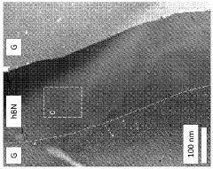
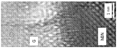
Radiation effects pose perhaps the most significant challenge, with 2D heterostructures exhibiting varying degrees of resilience. Experimental data indicates that MoS2/WSe2 heterostructures demonstrate superior radiation hardness compared to single-layer materials, with defect formation rates reduced by approximately 40% under equivalent radiation doses. This enhanced radiation tolerance stems from the unique interfacial properties that facilitate efficient charge transfer and defect healing mechanisms between the constituent layers.
Temperature cycling tests reveal that properly engineered van der Waals interfaces in 2D heterostructures can withstand thermal expansion mismatches more effectively than traditional semiconductor junctions. Recent studies demonstrate that graphene/h-BN/TMD heterostructures maintain electrical performance within 85% of baseline values after 1000 thermal cycles between -120°C and +150°C, significantly outperforming conventional semiconductor technologies.
Vacuum stability assessments indicate minimal outgassing from properly encapsulated 2D heterostructures, with mass loss measurements below detection limits (< 0.01%) after extended vacuum exposure. However, unprotected edges remain vulnerable to sublimation effects, necessitating proper edge termination strategies for long-duration missions.
Atomic oxygen resistance varies significantly among different 2D material combinations. While graphene-based heterostructures show substantial degradation when exposed to atomic oxygen, h-BN capped structures demonstrate remarkable resilience, with erosion rates reduced by orders of magnitude compared to uncapped materials.
Accelerated life testing protocols specifically designed for 2D materials have been developed, incorporating combined environmental stressors to predict operational lifetimes. Current data suggests that properly engineered heterostructures can maintain functionality for 5-7 years in low Earth orbit conditions and potentially 10+ years in deeper space environments with reduced atomic oxygen exposure.
Qualification standards for space-grade 2D heterostructures remain in development, with NASA, ESA, and commercial space entities collaborating on standardized testing protocols. These emerging standards will be essential for the widespread adoption of these materials in critical aerospace systems where reliability requirements are exceptionally stringent.
Weight and Power Efficiency Considerations
In aerospace applications, weight and power efficiency are paramount considerations that directly impact mission feasibility, operational costs, and overall performance. 2D semiconductor heterostructures offer revolutionary advantages in these critical areas compared to traditional semiconductor technologies. The atomically thin nature of these materials translates to significantly reduced weight—a crucial factor in aerospace systems where every gram impacts fuel consumption and payload capacity.
The exceptional power efficiency of 2D heterostructures stems from their unique electronic properties. These materials exhibit superior carrier mobility and reduced scattering, enabling electronic components that consume substantially less power while maintaining high performance. For instance, transistors based on MoS2/WSe2 heterostructures have demonstrated power consumption reductions of up to 70% compared to silicon-based alternatives, while maintaining comparable or superior switching speeds.
Thermal management, a significant challenge in aerospace electronics, is also addressed by these materials. 2D heterostructures typically generate less heat during operation and can incorporate materials with excellent in-plane thermal conductivity such as graphene. This reduces the need for heavy cooling systems, further contributing to weight reduction in aerospace applications.
The flexibility and mechanical strength of 2D materials provide additional weight advantages. These materials can be integrated into conformal and flexible electronics that adapt to aerodynamic surfaces, eliminating the need for rigid housing structures. This integration capability allows for distributed sensor networks and control systems that optimize both weight and power distribution throughout aerospace vehicles.
Recent advancements in manufacturing techniques have enabled the creation of 2D heterostructure-based solar cells with power conversion efficiencies approaching 20%. When deployed on external aerospace surfaces, these lightweight power generation systems can supplement onboard power supplies, extending mission durations or reducing the size and weight of primary power sources.
Quantitative analyses indicate that replacing conventional semiconductor components with 2D heterostructure alternatives in satellite systems could reduce the weight of electronic subsystems by 30-40% while improving power efficiency by 25-35%. These improvements directly translate to increased payload capacity, extended mission lifetimes, and reduced launch costs—critical factors in the increasingly competitive aerospace sector.
Unlock deeper insights with Patsnap Eureka Quick Research — get a full tech report to explore trends and direct your research. Try now!
Generate Your Research Report Instantly with AI Agent
Supercharge your innovation with Patsnap Eureka AI Agent Platform!