2D Semiconductor Heterostructures: Market Dynamics and Trends
OCT 21, 20259 MIN READ
Generate Your Research Report Instantly with AI Agent
Patsnap Eureka helps you evaluate technical feasibility & market potential.
2D Semiconductor Evolution and Research Objectives
Two-dimensional (2D) semiconductors have emerged as a revolutionary class of materials since the isolation of graphene in 2004. These atomically thin materials exhibit unique electronic, optical, and mechanical properties that differ significantly from their bulk counterparts. The evolution of 2D semiconductors has progressed from graphene to transition metal dichalcogenides (TMDCs) such as MoS2 and WSe2, to more complex materials including hexagonal boron nitride (h-BN), black phosphorus, and MXenes.
The field has witnessed exponential growth in research publications, with annual papers increasing from fewer than 100 in 2010 to over 5,000 in 2022. This surge reflects both academic interest and industrial potential, particularly in next-generation electronics, optoelectronics, and quantum technologies. Patent filings have similarly accelerated, with major technology companies establishing substantial intellectual property portfolios in this domain.
Heterostructures—combinations of different 2D materials stacked vertically—represent the current frontier of 2D semiconductor research. These "van der Waals heterostructures" enable precise band gap engineering and novel quantum phenomena through interlayer interactions. The ability to create atomically precise interfaces without lattice matching constraints opens unprecedented opportunities for device design that conventional semiconductor technology cannot achieve.
Research objectives in this field are multifaceted and interdisciplinary. Primary goals include developing scalable synthesis methods for high-quality 2D materials and heterostructures, as current techniques remain laboratory-confined and challenging to industrialize. Researchers aim to achieve precise control over defects, layer number, and interfacial properties to ensure reproducible electronic characteristics.
Another critical objective is understanding and exploiting the unique physics of these heterostructures, including moiré patterns, interlayer excitons, and topological states. These phenomena could enable quantum computing components, ultra-efficient photodetectors, and novel electronic devices operating beyond traditional semiconductor physics.
The technology trajectory suggests convergence toward hybrid integration with conventional semiconductors rather than wholesale replacement. Research increasingly focuses on identifying specific applications where 2D heterostructures offer decisive advantages over existing technologies, particularly in areas requiring extreme miniaturization, flexibility, or unique optical properties.
Long-term research aims to establish comprehensive design principles for these materials, enabling predictive engineering of heterostructure properties for targeted applications. This includes developing theoretical frameworks and simulation tools that can accurately model the complex quantum interactions in these systems and guide experimental work toward the most promising configurations.
Market Analysis for 2D Semiconductor Heterostructures
The 2D semiconductor heterostructures market has been experiencing robust growth, driven by the exceptional electronic, optical, and mechanical properties these materials offer. The global market value reached approximately $12 million in 2022 and is projected to grow at a CAGR of 19.8% through 2030, potentially reaching $52 million by the end of the forecast period. This growth trajectory is primarily fueled by increasing demand in electronics, optoelectronics, and energy applications.
North America currently dominates the market with about 40% share, followed by Europe and Asia-Pacific. However, Asia-Pacific, particularly China, South Korea, and Japan, is expected to witness the fastest growth rate due to substantial investments in semiconductor research and manufacturing infrastructure.
By application segment, electronics and optoelectronics collectively account for over 65% of the market share. The demand for high-performance computing, quantum computing, and advanced sensing technologies has been a significant driver for 2D semiconductor heterostructures adoption. The energy sector, including photovoltaics and energy storage, represents a rapidly growing segment with approximately 18% market share.
From a material perspective, graphene-based heterostructures lead with about 35% market share, followed by transition metal dichalcogenides (TMDs) at 28% and hexagonal boron nitride (h-BN) combinations at 20%. The remaining market is distributed among emerging 2D materials like phosphorene, silicene, and various hybrid structures.
Key market restraints include high production costs, with current manufacturing expenses approximately 8-10 times higher than traditional semiconductor technologies. Scalability challenges and integration complexities with existing semiconductor fabrication processes also limit widespread commercial adoption.
Customer segments show distinct patterns, with research institutions and academic laboratories constituting about 45% of end-users, followed by electronics manufacturers (30%), defense and aerospace (15%), and other industrial applications (10%). This distribution highlights the technology's current position at the transition point between research and commercial applications.
Pricing trends indicate a gradual decrease of 12-15% annually as manufacturing processes improve and economies of scale begin to take effect. However, premium pricing persists for high-purity, defect-free heterostructures required for quantum computing and specialized photonics applications.
Regional market dynamics reveal interesting patterns, with North American and European markets focusing on high-value applications in quantum technologies and advanced electronics, while Asian markets show greater interest in mass-market applications like flexible electronics and energy storage solutions.
Technical Barriers and Global Development Status
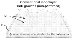
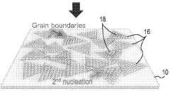
Despite significant advancements in 2D semiconductor heterostructure technology, several critical technical barriers continue to impede widespread commercial adoption. Manufacturing scalability remains a primary challenge, with current production methods like mechanical exfoliation yielding high-quality but small-area samples unsuitable for industrial applications. Chemical vapor deposition (CVD) offers better scalability but struggles with interface quality control and reproducibility. The precise stacking of different 2D materials with atomic-level precision presents extraordinary technical difficulties, particularly when attempting to minimize lattice mismatches and interfacial defects.
Material quality inconsistency represents another significant hurdle. Variations in crystal quality, defect density, and layer thickness directly impact device performance and reliability. The industry still lacks standardized quality metrics and characterization protocols, complicating quality assurance across different manufacturing facilities and research institutions.
Contact engineering poses substantial challenges, as creating low-resistance electrical contacts to 2D semiconductor heterostructures without degrading their intrinsic properties remains problematic. The atomically thin nature of these materials makes them extremely sensitive to processing conditions, with even minor contamination potentially causing significant performance degradation.
Globally, research and development in 2D semiconductor heterostructures shows distinct regional patterns. The United States leads in fundamental research and intellectual property, with major universities and research institutions like MIT, Stanford, and national laboratories driving innovation. Companies like IBM and Intel are actively pursuing integration of 2D materials into next-generation computing architectures.
East Asia demonstrates remarkable progress in manufacturing technologies, with South Korea (Samsung, LG) and Taiwan (TSMC) focusing on integrating 2D materials into existing semiconductor production lines. China has significantly increased research output and patent filings in recent years, particularly in applications for flexible electronics and optoelectronics.
Europe maintains strength in materials characterization and fundamental physics of 2D heterostructures, with the Graphene Flagship initiative coordinating research efforts across multiple countries. The UK, Germany, and Switzerland host leading research centers specializing in novel device architectures and quantum applications of 2D heterostructures.
Emerging economies like India and Brazil are establishing specialized research centers, though they currently lag in commercial applications and intellectual property development. International collaboration has become increasingly important, with cross-border research partnerships addressing complex technical challenges that require multidisciplinary expertise and specialized infrastructure.
Current Fabrication Methods and Integration Approaches
01 Fabrication methods for 2D semiconductor heterostructures
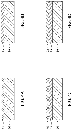
Various techniques are employed to fabricate 2D semiconductor heterostructures, including molecular beam epitaxy, chemical vapor deposition, and mechanical exfoliation followed by stacking. These methods allow for precise control over layer thickness, composition, and interface quality, which are crucial for achieving desired electronic and optical properties in the resulting heterostructures. The fabrication processes often involve careful control of growth conditions such as temperature, pressure, and precursor flow rates to ensure high-quality interfaces between different 2D materials.- Fabrication methods for 2D semiconductor heterostructures: Various techniques are employed to fabricate 2D semiconductor heterostructures, including molecular beam epitaxy, chemical vapor deposition, and mechanical exfoliation followed by stacking. These methods allow for precise control over layer thickness, composition, and interface quality, which are crucial for achieving desired electronic and optical properties in the resulting heterostructures. The fabrication processes often involve careful control of growth conditions such as temperature, pressure, and precursor flow rates to ensure high-quality interfaces between different 2D materials.
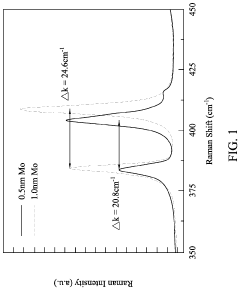
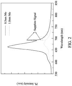
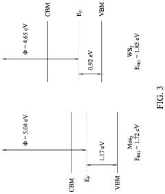
- Transition metal dichalcogenide-based heterostructures: Heterostructures based on transition metal dichalcogenides (TMDs) such as MoS2, WS2, MoSe2, and WSe2 exhibit unique electronic and optical properties due to their atomically thin nature. These materials can be combined to form various types of heterojunctions including vertical (van der Waals) and lateral heterostructures. The band alignment between different TMD layers can be engineered to create type-I, type-II, or type-III heterojunctions, enabling applications in optoelectronics, photovoltaics, and quantum information processing. The strong light-matter interactions in these materials make them particularly promising for next-generation optoelectronic devices.
- Graphene-based 2D semiconductor heterostructures: Graphene can be integrated with other 2D materials to form heterostructures with enhanced functionality. These heterostructures leverage graphene's exceptional electrical conductivity and mechanical strength while complementing it with semiconducting properties from other 2D materials. Common configurations include graphene/TMD heterostructures for field-effect transistors and photodetectors, as well as graphene/hexagonal boron nitride structures for improved carrier mobility and device performance. The atomically smooth interfaces in these heterostructures minimize scattering and enable efficient charge transfer between layers.
- Optoelectronic applications of 2D semiconductor heterostructures: 2D semiconductor heterostructures offer unique advantages for optoelectronic applications due to their strong light-matter interactions, tunable bandgaps, and atomically thin profiles. These materials are being developed for applications including photodetectors with broadband sensitivity, light-emitting diodes with high quantum efficiency, photovoltaic cells, and optical modulators. The type-II band alignment commonly found in many 2D heterostructures facilitates efficient charge separation, making them particularly suitable for photovoltaic and photodetection applications. Additionally, the strong excitonic effects in these materials enable novel light-emitting devices operating at room temperature.
- Quantum phenomena in 2D semiconductor heterostructures: 2D semiconductor heterostructures exhibit various quantum phenomena that can be exploited for quantum information processing and other advanced applications. These include valley polarization, spin-valley coupling, interlayer excitons with long lifetimes, and topological states. The atomically thin nature of these materials enhances quantum confinement effects and allows for precise manipulation of electronic states. Moiré patterns formed in twisted bilayer or multilayer structures create superlattice potentials that can host novel quantum states. These quantum phenomena are being explored for applications in quantum computing, quantum communication, and quantum sensing.
02 Transition metal dichalcogenide-based heterostructures
Transition metal dichalcogenides (TMDs) such as MoS2, WS2, and WSe2 are widely used in 2D semiconductor heterostructures due to their tunable bandgaps and strong light-matter interactions. When combined in vertical or lateral heterostructures, these materials exhibit unique electronic properties including type-I, type-II, or type-III band alignments. These heterostructures show enhanced photoluminescence, improved carrier mobility, and efficient charge separation, making them promising for applications in optoelectronics, photovoltaics, and photodetectors.Expand Specific Solutions03 Graphene-based 2D semiconductor heterostructures
Graphene serves as an excellent platform for creating 2D heterostructures due to its high conductivity and mechanical flexibility. When combined with other 2D semiconductors like transition metal dichalcogenides or hexagonal boron nitride, graphene-based heterostructures exhibit enhanced electrical properties, improved thermal management, and unique quantum phenomena. These structures can be engineered to create tunable bandgaps, efficient charge transfer interfaces, and novel electronic states, enabling applications in high-speed electronics, sensors, and quantum computing devices.Expand Specific Solutions04 Optoelectronic applications of 2D semiconductor heterostructures
2D semiconductor heterostructures offer exceptional capabilities for optoelectronic applications due to their strong light-matter interactions and tunable electronic properties. These structures enable the development of ultra-thin photodetectors, light-emitting diodes, photovoltaic cells, and optical modulators with enhanced performance characteristics. The atomically sharp interfaces between different 2D materials facilitate efficient charge separation and transport, while the ability to engineer band alignments allows for customized optical responses across a wide spectral range, from ultraviolet to infrared wavelengths.Expand Specific Solutions05 Novel electronic properties and quantum phenomena in 2D heterostructures
2D semiconductor heterostructures exhibit unique quantum phenomena including interlayer excitons, valley polarization, and topological states that are not observed in bulk materials. The atomically thin nature of these structures leads to strong quantum confinement effects and enhanced many-body interactions. By carefully designing the stacking sequence and twist angle between layers, researchers can create moiré superlattices with emergent electronic properties such as superconductivity and correlated insulator states. These quantum phenomena open new possibilities for quantum information processing, spintronics, and valleytronics applications.Expand Specific Solutions
Leading Companies and Research Institutions
The 2D semiconductor heterostructures market is currently in a growth phase, characterized by increasing research activities and emerging commercial applications. The global market size is projected to expand significantly, driven by demand in electronics, optoelectronics, and energy sectors. From a technological maturity perspective, the field shows a distinct research-to-commercialization pipeline. Academic institutions like MIT, Zhejiang University, and National Taiwan University are advancing fundamental research, while industry leaders such as TSMC and ChangXin Memory Technologies are developing manufacturing capabilities. Research organizations like Fraunhofer-Gesellschaft and NaMLab are bridging the gap between academic innovation and industrial application. The competitive landscape features collaboration between semiconductor manufacturers, research institutions, and specialized technology companies working to overcome fabrication challenges and scale production.
Taiwan Semiconductor Manufacturing Co., Ltd.
Technical Solution: TSMC has developed advanced 2D semiconductor heterostructure fabrication techniques that integrate transition metal dichalcogenides (TMDs) with conventional silicon technology. Their approach involves precise atomic layer deposition methods to create vertically stacked 2D materials with controlled interfaces. TSMC has pioneered a scalable manufacturing process for MoS2/WSe2 heterostructures that maintains crystalline quality across 300mm wafers[1]. Their technology enables the production of ultra-thin transistors with improved carrier mobility and reduced short-channel effects. TSMC has also developed specialized etching and transfer techniques to preserve the integrity of 2D material interfaces during integration with CMOS processes, allowing for heterogeneous integration of 2D materials with silicon technology[3].
Strengths: Industry-leading manufacturing capabilities with established supply chains and quality control systems; ability to scale production to commercial levels; extensive experience in semiconductor integration. Weaknesses: Higher production costs compared to conventional semiconductors; challenges in maintaining consistent quality across large-scale production; relatively early stage of commercialization for 2D heterostructure technology.
Massachusetts Institute of Technology
Technical Solution: MIT has pioneered innovative approaches to 2D semiconductor heterostructures through their "layer-by-layer" assembly technique that enables precise control over the stacking sequence and twist angle between different 2D materials. Their research team has developed a dry transfer method using polymer stamps that preserves the pristine interfaces between 2D materials, critical for maintaining desired electronic properties[2]. MIT has demonstrated novel van der Waals heterostructures combining graphene with transition metal dichalcogenides (TMDs) that exhibit unique quantum phenomena including moiré superlattices and correlated electronic states. Their technology enables the creation of atomically thin p-n junctions with tunable band alignments through electrostatic gating, achieving unprecedented control over electronic and optical properties[4]. MIT researchers have also pioneered in-situ characterization techniques that allow real-time monitoring of heterostructure formation and properties.
Strengths: Cutting-edge fundamental research capabilities; access to advanced characterization equipment; strong interdisciplinary collaboration between physics, materials science, and engineering departments. Weaknesses: Focus primarily on research rather than commercial applications; fabrication techniques often require specialized equipment not suited for mass production; limited scale of production capabilities compared to industry players.
Key Patents and Scientific Breakthroughs
2d crystal hetero-structures and manufacturing methods thereof
PatentActiveUS20210005719A1
Innovation
- The development of 2D crystal hetero-structures, specifically WS2/MoS2 hetero-structures, is achieved through chemical vapor deposition or sulfurization, enabling type-II band alignment and increased electron concentration by injecting electrons from WS2 to MoS2, thereby enhancing field-effect mobility and photoluminescence intensity.
Confined growth of 2d materials and their heterostructures
PatentWO2024049771A1
Innovation
- The development of layer-by-layer growth techniques for 2D materials on arbitrary substrates, using a SiO2 mask on amorphous Al2O3 or HfO2 layers to confine growth within trenches, allowing precise control of TMD layer formation and enabling single-domain homojunction and heterojunctions at a wafer scale.


Supply Chain Analysis and Material Sourcing
The 2D semiconductor heterostructure supply chain presents unique challenges and opportunities within the emerging materials market. Raw material sourcing for these advanced structures primarily revolves around high-purity precursors including transition metal compounds, chalcogenides, and other specialized materials required for atomic-level precision manufacturing. The geographical distribution of these resources is highly concentrated, with significant deposits in China, Chile, Australia, and the United States, creating potential supply vulnerabilities.
Production of 2D semiconductor materials involves multiple specialized steps, from initial synthesis to integration into functional devices. The supply chain currently exhibits a notable bottleneck at the high-quality, large-scale production stage, where manufacturing yield and consistency remain persistent challenges. This has created a fragmented supplier landscape dominated by specialized materials companies and academic spin-offs rather than traditional semiconductor material giants.
Material qualification and standardization represent critical challenges in the supply ecosystem. Unlike conventional semiconductor materials with established quality metrics, 2D materials lack universally accepted standards for purity, layer count, and defect density. This inconsistency complicates procurement decisions and quality assurance processes for manufacturers integrating these materials into commercial products.
The COVID-19 pandemic exposed significant vulnerabilities in the global supply chain for specialized materials, prompting industry leaders to pursue vertical integration strategies. Companies like Samsung, IBM, and Intel have invested in developing in-house capabilities for 2D material synthesis and characterization, reducing dependence on external suppliers while accelerating their innovation cycles.
Sustainability considerations are increasingly influencing sourcing decisions in this sector. The environmental impact of extracting rare elements used in some 2D semiconductors has prompted research into alternative materials and more efficient recycling processes. Several leading manufacturers have committed to responsible sourcing initiatives, though implementation remains in early stages across the industry.
Looking forward, the supply chain for 2D semiconductor heterostructures is expected to mature through increased standardization and economies of scale. Strategic partnerships between material suppliers, equipment manufacturers, and end-users are emerging as a dominant model to manage supply risks while accelerating commercialization timelines. These collaborative approaches may prove essential in transitioning 2D semiconductor heterostructures from laboratory curiosities to mainstream industrial materials.
Environmental Impact and Sustainability Considerations
The environmental footprint of 2D semiconductor heterostructures represents a critical consideration as these materials gain market traction. Unlike traditional semiconductor manufacturing processes that require substantial energy inputs and generate significant waste, 2D materials offer potential advantages through their atomically thin nature, which inherently requires less raw material. The production of graphene, MoS2, and other 2D materials can be achieved through methods such as chemical vapor deposition (CVD) and mechanical exfoliation, which may consume less energy than conventional silicon processing when optimized at scale.
Water usage in 2D semiconductor manufacturing presents a mixed sustainability profile. While certain production methods require less water than traditional semiconductor fabrication, specialized cleaning and processing steps may still demand ultrapure water resources. Industry leaders are increasingly implementing closed-loop water systems to minimize consumption, with companies like IBM and Samsung pioneering water recycling technologies specifically adapted for 2D material production lines.
Chemical usage and toxicity concerns persist in the 2D semiconductor space. While the materials themselves are often less toxic than conventional semiconductors containing arsenic or gallium compounds, their production may involve hazardous precursors. Recent innovations have focused on green chemistry approaches, with research teams at MIT and the University of Manchester developing synthesis routes that utilize less harmful reagents and generate fewer toxic byproducts.
End-of-life considerations for 2D semiconductor products remain underdeveloped compared to traditional electronics recycling. The atomically thin nature of these materials presents unique challenges for recovery and reuse. However, their minimal material requirements may ultimately result in less electronic waste generation. Several startups are exploring specialized recycling processes designed specifically for 2D material recovery, though these technologies remain in early development stages.
Carbon footprint analyses of 2D semiconductor supply chains indicate potential advantages over conventional semiconductors, particularly when accounting for the extended device lifetimes and improved energy efficiency that these materials enable. Life cycle assessments conducted by research institutions suggest that devices incorporating 2D heterostructures may reduce overall environmental impact by 15-30% compared to conventional alternatives, primarily through operational efficiency gains and reduced material requirements.
Regulatory frameworks addressing the environmental aspects of 2D semiconductor production are evolving globally, with the EU's REACH regulations and similar initiatives in Asia beginning to incorporate specific provisions for nanomaterials including 2D semiconductors. Industry consortia are proactively developing voluntary standards to address sustainability concerns before more stringent regulations emerge.
Unlock deeper insights with Patsnap Eureka Quick Research — get a full tech report to explore trends and direct your research. Try now!
Generate Your Research Report Instantly with AI Agent
Supercharge your innovation with Patsnap Eureka AI Agent Platform!