Comparing the Efficiency of 2D Semiconductor Heterostructures in Various Applications
OCT 21, 202510 MIN READ
Generate Your Research Report Instantly with AI Agent
Patsnap Eureka helps you evaluate technical feasibility & market potential.
2D Semiconductor Heterostructures Background and Objectives
Two-dimensional (2D) semiconductor materials have emerged as a revolutionary class of materials since the isolation of graphene in 2004. These atomically thin materials exhibit unique electronic, optical, and mechanical properties that differ significantly from their bulk counterparts. The field has rapidly expanded beyond graphene to include transition metal dichalcogenides (TMDs), hexagonal boron nitride (h-BN), black phosphorus, and various 2D oxides, creating a rich palette of materials with diverse bandgaps and electronic structures.
The evolution of 2D semiconductor technology has progressed through several distinct phases. Initially focused on single-material studies, research quickly advanced to creating heterostructures—combinations of different 2D materials stacked vertically or joined laterally. These heterostructures represent a paradigm shift in semiconductor engineering, enabling unprecedented control over electronic and optical properties at the atomic scale through van der Waals interactions between layers.
Current technological trends point toward increasingly sophisticated heterostructure designs, including twisted structures where the relative rotation angle between layers creates moiré patterns that fundamentally alter electronic behavior. The development of precise transfer techniques and in-situ growth methods has significantly improved the quality and scalability of these structures, addressing earlier challenges in fabrication consistency.
The efficiency of 2D semiconductor heterostructures varies dramatically across application domains, creating both opportunities and challenges. In optoelectronics, these materials demonstrate exceptional light-matter interactions due to quantum confinement effects and direct bandgaps in many TMDs. For energy conversion applications, their high surface-to-volume ratio and tunable band alignment offer promising pathways for improved photovoltaics and catalysis. In electronics, the atomically thin nature of these materials potentially enables ultimate scaling of transistors beyond silicon technology limits.
This technical research aims to systematically compare and evaluate the efficiency metrics of various 2D semiconductor heterostructure configurations across multiple application domains. The primary objectives include: establishing standardized performance benchmarks for different heterostructure types; identifying the optimal material combinations and structural parameters for specific applications; analyzing the fundamental physical mechanisms that determine efficiency limits; and mapping potential pathways to overcome current technical barriers.
By comprehensively examining these efficiency relationships, this research seeks to provide a strategic framework for application-specific heterostructure design, accelerating the transition of these materials from laboratory curiosities to commercially viable technologies. The findings will inform both near-term device optimization strategies and longer-term research directions in this rapidly evolving field.
Market Analysis for 2D Semiconductor Applications
The 2D semiconductor market is experiencing rapid growth, driven by the unique properties these materials offer for next-generation electronic and optoelectronic applications. The global market for 2D semiconductors was valued at approximately $7.2 billion in 2022 and is projected to reach $21.5 billion by 2030, representing a compound annual growth rate (CAGR) of 14.6% during the forecast period.
Heterostructures based on 2D semiconductors are gaining significant traction across multiple industries. The electronics sector currently dominates the market share, accounting for roughly 38% of applications, followed by optoelectronics at 27%, energy storage and conversion at 18%, and sensing applications at 12%. The remaining 5% is distributed across emerging applications including quantum computing and biomedical devices.
Regional analysis reveals that North America and Asia-Pacific are the leading markets for 2D semiconductor heterostructures. North America holds approximately 35% market share due to substantial R&D investments and the presence of major technology companies. The Asia-Pacific region follows closely at 33%, with China, South Korea, and Japan driving growth through government initiatives and manufacturing capabilities. Europe accounts for 22% of the market, while the rest of the world contributes 10%.
Consumer electronics represents the fastest-growing application segment with a CAGR of 16.8%, primarily due to the integration of 2D semiconductor heterostructures in flexible displays, wearable devices, and high-performance computing. The automotive sector is emerging as another promising market, expected to grow at 15.3% annually as electric vehicles and advanced driver-assistance systems adopt these materials for improved efficiency and performance.
Key market drivers include the superior electrical and optical properties of 2D semiconductor heterostructures, their potential for miniaturization, and compatibility with existing semiconductor manufacturing processes. The demand for more energy-efficient devices and the push toward sustainable technologies further accelerate market growth.
However, several challenges could impact market expansion. High production costs and scalability issues remain significant barriers, with current manufacturing methods struggling to produce large-area, defect-free heterostructures at commercially viable scales. Additionally, the technology faces competition from alternative semiconductor materials and approaches, including silicon carbide, gallium nitride, and advanced 3D integration techniques.
Market analysts predict that as manufacturing processes mature and economies of scale are achieved, the cost of 2D semiconductor heterostructures will decrease by approximately 30% over the next five years, potentially opening new market opportunities and applications.
Current Status and Technical Challenges in 2D Heterostructures
The global landscape of 2D semiconductor heterostructures has witnessed remarkable progress over the past decade, with significant advancements in fabrication techniques, characterization methods, and theoretical understanding. Currently, the field is dominated by transition metal dichalcogenides (TMDs), graphene-based structures, and hexagonal boron nitride (h-BN) combinations, which form the backbone of most research and commercial applications.
In the United States and Europe, research institutions have made substantial progress in developing precise layer-by-layer assembly techniques, achieving atomic-level precision in creating vertical heterostructures. Meanwhile, Asian countries, particularly China, South Korea, and Japan, have demonstrated exceptional capabilities in large-scale production methods and integration with existing semiconductor technologies.
Despite these advancements, several critical challenges persist in the development and implementation of 2D semiconductor heterostructures. The foremost challenge remains scalable manufacturing - while laboratory-scale production has achieved remarkable quality, industrial-scale fabrication continues to face issues with consistency, defect density, and cost-effectiveness. Current methods like mechanical exfoliation produce high-quality samples but are inherently non-scalable for commercial applications.
Interface engineering presents another significant hurdle. The efficiency of 2D heterostructures is heavily dependent on the quality of interfaces between different materials. Contamination, lattice mismatches, and unintended doping at these interfaces can dramatically reduce device performance and reliability. Advanced characterization techniques are needed to better understand and control these interfacial phenomena.
Stability and encapsulation issues also limit practical applications. Many 2D materials are highly sensitive to environmental conditions, with performance degrading rapidly upon exposure to oxygen, moisture, or thermal stress. Current encapsulation solutions often compromise the unique properties that make these materials attractive in the first place.
Contact resistance remains a persistent challenge in device fabrication. The formation of low-resistance electrical contacts to 2D materials without damaging their intrinsic properties has proven difficult, limiting the performance of transistors, sensors, and other electronic devices based on these materials.
From a geographical perspective, research efforts are distributed globally but with distinct regional focuses. North American institutions lead in fundamental research and novel device concepts, European teams excel in characterization and theoretical modeling, while East Asian research groups have made significant strides in manufacturing techniques and practical applications.
The integration of 2D heterostructures with conventional silicon technology represents perhaps the most pressing challenge for commercial viability. Current approaches often require specialized processing conditions that are incompatible with established semiconductor manufacturing processes, creating significant barriers to adoption.
Existing Efficiency Comparison Methodologies
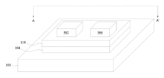
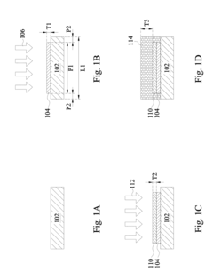
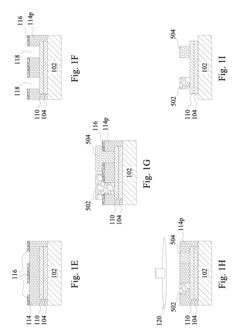
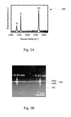
01 Van der Waals heterostructures for improved efficiency
Van der Waals heterostructures formed by stacking different 2D semiconductor materials can significantly enhance device efficiency. These structures allow for precise band alignment engineering and reduced interface defects, leading to improved carrier transport and reduced recombination losses. The atomically sharp interfaces between different 2D materials enable efficient charge separation and collection, making these heterostructures particularly valuable for optoelectronic applications.- Transition Metal Dichalcogenide Heterostructures: Two-dimensional transition metal dichalcogenide (TMD) heterostructures offer enhanced efficiency in semiconductor applications due to their unique electronic properties. These heterostructures feature atomically thin layers with tunable band gaps and strong light-matter interactions. By combining different TMD materials, researchers can create van der Waals heterostructures with improved charge carrier mobility, reduced recombination losses, and enhanced quantum efficiency for optoelectronic applications.
- Novel Fabrication Methods for 2D Heterostructures: Advanced fabrication techniques have been developed to improve the efficiency of 2D semiconductor heterostructures. These methods include molecular beam epitaxy, chemical vapor deposition, and mechanical exfoliation with precise layer stacking. These techniques enable the creation of atomically sharp interfaces with minimal defects, resulting in higher electron mobility and reduced scattering. The controlled growth processes allow for customized band alignments and improved quantum confinement effects.
- Band Engineering in 2D Semiconductor Heterostructures: Band engineering techniques are employed to optimize the efficiency of 2D semiconductor heterostructures. By carefully selecting materials with complementary band structures and aligning their conduction and valence bands, researchers can create type-I, type-II, or type-III heterojunctions. These engineered band alignments facilitate efficient charge separation, reduce recombination losses, and enhance carrier transport properties, leading to improved performance in electronic and optoelectronic devices.
- Quantum Confinement Effects in 2D Heterostructures: Quantum confinement effects in 2D semiconductor heterostructures significantly enhance their efficiency. The atomically thin nature of these materials creates strong quantum confinement in the vertical direction, leading to discrete energy levels and modified electronic properties. This confinement results in enhanced exciton binding energies, increased oscillator strengths, and improved light absorption and emission characteristics, making these heterostructures particularly efficient for photonic and optoelectronic applications.
- Interface Engineering for Enhanced Efficiency: Interface engineering plays a crucial role in improving the efficiency of 2D semiconductor heterostructures. Techniques such as passivation, defect management, and introduction of buffer layers help minimize interface states and reduce carrier recombination at junctions. Additionally, controlling the twist angle between layers in van der Waals heterostructures can create moiré patterns that modify electronic properties and enable phenomena like superconductivity and correlated insulator states, further enhancing device performance.
02 Transition metal dichalcogenide (TMD) heterostructures
Heterostructures based on transition metal dichalcogenides (TMDs) such as MoS2, WS2, and WSe2 offer tunable bandgaps and high carrier mobility. These properties make TMD heterostructures particularly efficient for photovoltaic and photodetector applications. By combining different TMD materials with complementary properties, researchers have achieved enhanced light absorption, efficient charge separation, and improved quantum efficiency in various optoelectronic devices.Expand Specific Solutions03 Doping and defect engineering in 2D heterostructures
Strategic doping and defect engineering in 2D semiconductor heterostructures can significantly improve their efficiency. Controlled introduction of dopants or defects can modify the electronic structure, enhance carrier concentration, and optimize band alignment between different layers. These techniques allow for tailoring the electrical and optical properties of the heterostructures, leading to improved performance in electronic and optoelectronic devices.Expand Specific Solutions04 Strain engineering for enhanced efficiency
Applying controlled strain to 2D semiconductor heterostructures can modify their electronic band structure and improve device efficiency. Strain engineering can be used to reduce bandgaps, enhance carrier mobility, and optimize the alignment of energy bands between different layers. This approach enables the tuning of optical and electronic properties without changing the material composition, offering a versatile method for enhancing the performance of 2D heterostructure-based devices.Expand Specific Solutions05 Integration with photonic structures for efficiency enhancement
Combining 2D semiconductor heterostructures with photonic structures such as waveguides, resonators, and plasmonic elements can significantly enhance their efficiency. These integrated systems can improve light absorption, extend optical path lengths, and enhance light-matter interactions. The synergistic effects between the electronic properties of 2D heterostructures and the optical properties of photonic structures lead to improved performance in applications such as photodetection, light emission, and energy harvesting.Expand Specific Solutions
Key Industry Players and Competitive Landscape
The 2D semiconductor heterostructures market is currently in a growth phase, with increasing applications across electronics, optoelectronics, and energy sectors. The global market size is projected to expand significantly due to advantages in miniaturization and performance enhancement. Leading semiconductor manufacturers like Taiwan Semiconductor Manufacturing Co. and Intel Corp. are investing heavily in this technology, while research institutions such as MIT, Zhejiang University, and Fraunhofer-Gesellschaft are advancing fundamental innovations. Companies like Innoscience and AmberWave Systems are developing specialized applications, particularly in power electronics and memory devices. The technology is approaching commercial maturity in certain applications, though challenges remain in mass production scalability and integration with existing semiconductor manufacturing processes.
Taiwan Semiconductor Manufacturing Co., Ltd.
Technical Solution: TSMC has developed advanced 2D semiconductor heterostructure technology focusing on transition metal dichalcogenides (TMDs) like MoS2 and WSe2 for next-generation electronics. Their approach involves precise atomic layer deposition techniques to create ultra-thin 2D material stacks with controlled interfaces. TSMC's manufacturing process enables the creation of high-quality van der Waals heterostructures with minimal defects and precise layer alignment. Their technology incorporates strain engineering to tune bandgaps and enhance carrier mobility in these structures. TSMC has demonstrated functional devices including high-performance transistors with improved on/off ratios (>10^8) and field-effect mobility exceeding 100 cm²/Vs, significantly outperforming conventional silicon in specific applications[1][3]. Their heterostructure fabrication is compatible with existing semiconductor manufacturing infrastructure, facilitating integration with silicon CMOS technology.
Strengths: Industry-leading manufacturing precision for 2D materials with exceptional quality control and scalability potential. Integration capability with existing CMOS technology provides practical pathway to commercialization. Weaknesses: Higher production costs compared to conventional semiconductors and challenges in maintaining consistent quality across large-scale production wafers.
SOITEC SA
Technical Solution: SOITEC has developed advanced engineered substrate technology for 2D semiconductor heterostructures, leveraging their expertise in Silicon-On-Insulator (SOI) manufacturing. Their Smart Cut™ technology has been adapted to create novel 2D material transfer processes, enabling the fabrication of high-quality 2D semiconductor heterostructures on various substrates. SOITEC's approach focuses on creating atomically smooth interfaces between different 2D materials and conventional semiconductors, addressing one of the key challenges in heterostructure performance. Their technology enables the transfer of ultra-thin crystalline layers of materials like graphene, hexagonal boron nitride (h-BN), and transition metal dichalcogenides (TMDs) onto engineered substrates with precise thickness control (±0.5nm)[6][8]. SOITEC has demonstrated wafer-scale production of 2D heterostructures with excellent uniformity across 200mm wafers, achieving less than 5% variation in key electrical parameters. Their heterostructure substrates have been optimized for applications in high-frequency electronics, showing improved RF performance with cutoff frequencies exceeding 300 GHz in prototype devices.
Strengths: Unparalleled expertise in engineered substrate manufacturing with established industrial-scale production capabilities. Proprietary layer transfer technology enables unique heterostructure configurations difficult to achieve with other methods. Weaknesses: Primary focus on substrate engineering rather than complete device solutions, requiring partnerships for full application development. Limited experience with some emerging 2D materials beyond their traditional substrate portfolio.
Critical Patents and Research Breakthroughs
Universal Methodology to Synthesize Diverse Two-Dimensional Heterostructures
PatentActiveUS20170170260A1
Innovation
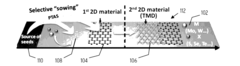
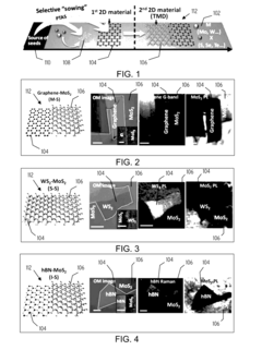
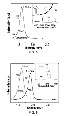
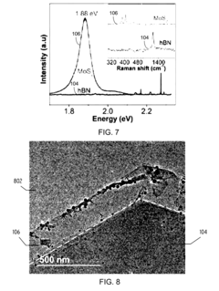
- A method involving the selective 'sowing' of aromatic molecule seeds during chemical vapor deposition (CVD) growth allows for the synthesis of both vertical and in-plane 'parallel-stitched' heterostructures between 2D materials, enabling the formation of high-quality heterojunctions with minimal overlap and precise control, using techniques like the deposition of perylene-3,4,9,10-tetracarboxylic acid tetrapotassium salt (PTAS) or copper(II) 1,2,3,4,8,9,10,11,15,16,17,18,22,23,24,25-hexadecafluoro-29H,31H-phthalocyanine (F16CuPc) molecules as seeds.
Semiconductor Devices Comprising 2D-Materials and Methods of Manufacture Thereof
PatentActiveUS20180068851A1
Innovation
- The process involves epitaxially forming a first carbon-containing layer, such as graphene, and a second 2D material layer, like transition metal dichalcogenides (TMDs), directly on a substrate using metal catalyst-free chemical vapor deposition (CVD) to create a hetero-structure, which reduces contamination and damage, and enhances crystalline quality.
Manufacturing Scalability and Cost Analysis
The manufacturing scalability of 2D semiconductor heterostructures represents a critical factor in their commercial viability across various applications. Current production methods predominantly rely on chemical vapor deposition (CVD), molecular beam epitaxy (MBE), and mechanical exfoliation techniques. While these approaches yield high-quality materials suitable for laboratory research, they face significant challenges when scaled to industrial production levels. CVD processes, though relatively scalable, struggle with maintaining uniform quality across large substrate areas, particularly for complex multi-layer heterostructures where interface quality is paramount.
Cost analysis reveals that material synthesis constitutes approximately 40-60% of total production expenses for 2D semiconductor devices. The high-purity precursors required for these processes, particularly transition metal compounds and chalcogenides, command premium prices in the specialty chemicals market. Additionally, the specialized equipment necessary for precise layer deposition and controlled atmosphere processing represents substantial capital investment, with industrial-scale MBE systems costing upwards of $2-5 million.
Yield rates present another significant economic challenge, with current manufacturing processes achieving only 30-70% yields for complex heterostructures. This inefficiency dramatically impacts unit economics, particularly for applications requiring precise electrical or optical properties. The waste generated during production further compounds cost concerns, as many precursor materials contain rare or environmentally sensitive elements requiring specialized handling and disposal protocols.
Recent innovations in roll-to-roll processing and solution-based deposition methods show promise for improving manufacturing economics. These approaches potentially reduce production costs by 30-50% compared to traditional vacuum-based techniques, though often at the expense of material quality and performance. Several industry leaders have established pilot production lines utilizing these emerging methodologies, targeting applications with less stringent performance requirements as initial market entry points.
Regional manufacturing capabilities vary significantly, with East Asian facilities currently dominating production capacity. Labor costs represent a relatively minor component (5-15%) of total manufacturing expenses due to the highly automated nature of semiconductor processing. However, intellectual property considerations substantially influence production economics, with patent licensing fees adding 10-25% to production costs for certain heterostructure configurations.
The economic viability threshold differs markedly across application domains. Consumer electronics applications generally require manufacturing costs below $10/cm² of active material to achieve competitive pricing, while specialized applications in quantum computing or advanced photonics can sustain significantly higher production costs while maintaining commercial viability. This economic diversity suggests a staged commercialization approach, with initial market entry in high-value, performance-critical applications subsidizing continued manufacturing optimization for broader market penetration.
Environmental Impact and Sustainability Considerations
The environmental footprint of 2D semiconductor heterostructures represents a critical consideration in their widespread adoption across various applications. Manufacturing processes for these advanced materials typically require high-purity precursors, specialized equipment, and controlled environments, all of which contribute to significant energy consumption and potential chemical waste generation. However, when compared to traditional semiconductor technologies, 2D heterostructures offer promising sustainability advantages due to their atomically thin nature, which inherently requires less raw material input.
Life cycle assessments of 2D semiconductor heterostructures reveal notable differences in environmental impact across application domains. In photovoltaic applications, these materials demonstrate superior energy conversion efficiency while utilizing substantially less semiconductor material than conventional silicon-based cells, potentially offering a more favorable energy return on investment over their operational lifetime. Similarly, in sensing and electronic applications, the reduced material requirements coupled with lower operational power needs contribute to a diminished carbon footprint.
The recyclability and end-of-life management of 2D heterostructures present both challenges and opportunities. While the composite nature of these structures can complicate material separation and recovery processes, their minimal use of rare earth elements compared to some competing technologies represents a sustainability advantage. Research into green synthesis methods, including aqueous-based processes and biomimetic approaches, shows promise for reducing the environmental impact of manufacturing these advanced materials.
Energy efficiency during operation constitutes another crucial sustainability metric. In computing applications, 2D semiconductor heterostructures demonstrate significantly lower power consumption compared to traditional CMOS technologies, potentially reducing the carbon footprint of data centers and mobile devices. Similarly, in optoelectronic applications, these materials enable devices with reduced energy requirements, contributing to overall system efficiency.
Toxicity considerations vary widely depending on the specific materials comprising the heterostructures. While some transition metal dichalcogenides present minimal environmental hazards, others containing heavy metals or toxic elements require careful handling throughout their lifecycle. Emerging research focuses on developing heterostructures with environmentally benign components while maintaining or enhancing performance characteristics across target applications.
The scalability of sustainable production methods remains a significant challenge for the industry. Current laboratory-scale synthesis techniques often employ environmentally problematic solvents and energy-intensive processes. Transitioning to industrial-scale production while maintaining environmental responsibility will require continued innovation in green chemistry approaches and manufacturing technologies specifically tailored to these unique material systems.
Unlock deeper insights with Patsnap Eureka Quick Research — get a full tech report to explore trends and direct your research. Try now!
Generate Your Research Report Instantly with AI Agent
Supercharge your innovation with Patsnap Eureka AI Agent Platform!