Technological Frontiers in Semiconductor Heterostructure Design
OCT 21, 20259 MIN READ
Generate Your Research Report Instantly with AI Agent
PatSnap Eureka helps you evaluate technical feasibility & market potential.
Semiconductor Heterostructure Evolution and Objectives
Semiconductor heterostructures have evolved significantly since their theoretical conception in the 1950s and practical implementation in the 1970s. The fundamental principle behind these structures involves the combination of different semiconductor materials with varying bandgaps to create interfaces that exhibit unique electronic and optical properties. This technological approach has revolutionized modern electronics, enabling the development of high-speed transistors, efficient light-emitting diodes, and sophisticated optoelectronic devices.
The evolution of semiconductor heterostructures can be traced through several distinct phases. Initially, the focus was on simple binary III-V compound semiconductor junctions, such as GaAs/AlGaAs. These early structures demonstrated the basic principles of band engineering but were limited by material quality and fabrication capabilities. The 1980s witnessed significant advancements in epitaxial growth techniques, particularly Molecular Beam Epitaxy (MBE) and Metal-Organic Chemical Vapor Deposition (MOCVD), which enabled the creation of more complex and precisely controlled heterostructures.
The 1990s marked the emergence of quantum well, quantum wire, and quantum dot structures, where carriers are confined in one, two, or three dimensions, respectively. These quantum-confined structures exhibited remarkable properties that could be tailored by adjusting their dimensions, compositions, and strain states. This period also saw the development of strained-layer superlattices and pseudomorphic heterostructures, which expanded the range of achievable material combinations.
In the 2000s, the field progressed toward more sophisticated designs incorporating multiple quantum wells, distributed Bragg reflectors, and resonant tunneling structures. The integration of heterostructures with silicon platforms became a significant focus, aiming to combine the advantages of III-V materials with the established silicon technology infrastructure.
Current research objectives in semiconductor heterostructure design are multifaceted. A primary goal is to develop novel material combinations that can overcome existing limitations in performance, efficiency, and reliability. This includes exploring wide-bandgap semiconductors like GaN and SiC for high-power applications, as well as narrow-bandgap materials for infrared detection and emission.
Another critical objective is the miniaturization and three-dimensional integration of heterostructure devices, which requires precise control over interfaces at the atomic scale. Researchers are also focusing on enhancing the functionality of heterostructures through the incorporation of additional physical phenomena, such as spin-orbit coupling for spintronic applications and topological states for quantum computing.
The ultimate aim is to develop "designer" heterostructures with tailored electronic, optical, and thermal properties that can address specific technological challenges in energy conversion, information processing, sensing, and communication systems.
Market Applications and Demand Analysis
The semiconductor heterostructure market has witnessed substantial growth driven by increasing demand across multiple sectors. The global market for semiconductor heterostructures was valued at approximately $25 billion in 2022 and is projected to reach $42 billion by 2028, representing a compound annual growth rate of 9.1%. This growth trajectory is primarily fueled by expanding applications in telecommunications, consumer electronics, and emerging quantum computing technologies.
Telecommunications remains the dominant application sector, accounting for nearly 35% of the total market share. The deployment of 5G infrastructure worldwide has significantly accelerated demand for high-frequency heterostructure devices, particularly those based on GaAs and GaN materials. As network providers continue to expand coverage and enhance data transmission capabilities, the requirement for advanced semiconductor heterostructures with superior electron mobility characteristics continues to rise.
Consumer electronics represents another substantial market segment, with smartphones and portable devices incorporating increasingly sophisticated heterostructure-based components. The trend toward miniaturization coupled with enhanced functionality has driven innovation in heterostructure design, particularly for power management and RF applications. Industry analysts predict that this sector will experience 12% annual growth through 2027, outpacing the overall market average.
Emerging applications in quantum computing and quantum information processing are creating new market opportunities. Though currently representing less than 5% of the total market, this segment is experiencing the fastest growth rate at approximately 22% annually. Research institutions and technology companies are investing heavily in heterostructure designs that can maintain quantum coherence at higher temperatures, potentially revolutionizing computational capabilities.
The automotive sector has emerged as a rapidly expanding market for semiconductor heterostructures, particularly with the transition toward electric vehicles and advanced driver assistance systems. Power electronics based on SiC and GaN heterostructures are increasingly replacing traditional silicon-based components, offering higher efficiency and thermal performance. This market segment is projected to grow at 15% annually through 2028.
Regional analysis reveals that Asia-Pacific dominates the market with approximately 45% share, followed by North America (28%) and Europe (20%). China's investments in semiconductor manufacturing capabilities have significantly altered supply chain dynamics, while Taiwan maintains its position as a critical manufacturing hub for advanced heterostructure technologies.
Customer demand increasingly focuses on heterostructures that offer improved power efficiency, reduced thermal issues, and enhanced reliability. The industry is witnessing a shift toward customized heterostructure designs tailored to specific application requirements, moving beyond standardized solutions. This trend is particularly evident in specialized applications such as aerospace, defense, and medical imaging technologies.
Current Challenges in Heterostructure Technology
Despite significant advancements in semiconductor heterostructure technology, several critical challenges continue to impede further progress in this field. The precise control of interface quality remains one of the most persistent obstacles. As heterostructures become increasingly complex with atomic-level precision requirements, maintaining atomically sharp interfaces between different semiconductor materials becomes exceedingly difficult due to interdiffusion, lattice mismatch, and thermal effects during growth processes.
Strain management presents another significant challenge. The lattice mismatch between different semiconductor materials creates strain at interfaces, which can lead to defect formation, dislocations, and ultimately performance degradation. While controlled strain can be beneficial for modifying electronic properties, uncontrolled strain often results in reliability issues and reduced device performance.
The scaling limitations of current fabrication technologies pose substantial barriers to heterostructure advancement. As dimensions approach the nanometer scale, quantum effects become more pronounced, and traditional fabrication methods reach their physical limits. Techniques like molecular beam epitaxy (MBE) and metal-organic chemical vapor deposition (MOCVD) face challenges in maintaining uniformity and precision at these scales.
Material compatibility issues further complicate heterostructure design. Not all semiconductor materials can be effectively integrated due to differences in thermal expansion coefficients, chemical reactivity, and processing requirements. This limitation restricts the possible material combinations and consequently constrains device functionality and performance envelopes.
Thermal management has emerged as a critical challenge, particularly for high-power and high-frequency applications. Heat dissipation becomes increasingly problematic as device dimensions shrink and power densities rise, leading to performance degradation and reliability concerns in advanced heterostructure devices.
Characterization and modeling limitations also hinder progress. Current analytical techniques struggle to provide accurate, non-destructive characterization of buried interfaces and quantum structures. Similarly, computational models often fail to capture the full complexity of quantum effects, defect interactions, and interface phenomena in heterostructures.
Cost and scalability concerns represent significant barriers to widespread commercial adoption. Many advanced heterostructure fabrication techniques remain expensive and difficult to scale to industrial production levels, limiting their application primarily to research environments or high-value niche applications rather than mass-market products.
State-of-the-Art Heterostructure Design Approaches
01 Quantum well heterostructures
Semiconductor heterostructures incorporating quantum wells are designed to confine carriers in one dimension, creating unique electronic and optical properties. These structures typically consist of thin layers of lower bandgap material sandwiched between higher bandgap materials, enabling quantum confinement effects. Such heterostructures are fundamental in optoelectronic devices like lasers, LEDs, and photodetectors, offering improved efficiency, wavelength tunability, and performance characteristics compared to conventional semiconductor devices.- Quantum well heterostructures for optoelectronic devices: Semiconductor heterostructures incorporating quantum wells are designed to enhance optoelectronic device performance. These structures consist of thin layers of semiconductor materials with different bandgaps, creating quantum confinement effects that improve light emission efficiency and wavelength control. Such heterostructures are fundamental in the development of lasers, LEDs, and photodetectors with superior performance characteristics including higher efficiency, lower threshold currents, and precise spectral output.
- III-V compound semiconductor heterostructures: III-V compound semiconductor materials are combined to form advanced heterostructures with tailored electronic and optical properties. These heterostructures utilize materials such as GaAs, InP, GaN, and their alloys to create devices with high electron mobility and efficient light emission. The bandgap engineering possible with these materials enables applications in high-frequency electronics, high-efficiency solar cells, and solid-state lighting technologies.
- 2D material-based heterostructures: Two-dimensional materials such as graphene, transition metal dichalcogenides, and hexagonal boron nitride are stacked to form novel heterostructures with unique properties. These atomically thin layers create van der Waals heterostructures with minimal interfacial defects, enabling new electronic, optoelectronic, and sensing applications. The ability to precisely control layer composition and stacking order allows for the engineering of band alignments and carrier transport properties not achievable in conventional semiconductor systems.
- Wide bandgap semiconductor heterostructures: Wide bandgap semiconductor materials such as GaN, SiC, and related alloys are used to create heterostructures for high-power and high-temperature applications. These heterostructures leverage the superior electrical properties of wide bandgap materials, including high breakdown voltage and thermal conductivity. The resulting devices can operate at higher voltages, frequencies, and temperatures than conventional silicon-based electronics, making them ideal for power electronics, RF applications, and harsh environment sensing.
- Heterostructures for quantum computing and spintronics: Specialized semiconductor heterostructures are designed to control and manipulate quantum states for applications in quantum computing and spintronics. These structures incorporate materials and interfaces that preserve spin coherence, enable quantum confinement of electrons, and facilitate quantum bit (qubit) operations. Advanced epitaxial growth techniques are used to create pristine interfaces with minimal defects, allowing for longer coherence times and more reliable quantum operations in next-generation quantum information processing systems.
02 III-V compound semiconductor heterostructures
These heterostructures utilize combinations of elements from groups III and V of the periodic table to create advanced semiconductor devices. Materials such as GaAs, InP, GaN, and their alloys are engineered into multilayer structures with precisely controlled compositions and interfaces. The resulting heterostructures exhibit superior electron mobility, direct bandgaps, and excellent optoelectronic properties, making them ideal for high-frequency electronics, high-efficiency solar cells, and solid-state lighting applications.Expand Specific Solutions03 2D material-based heterostructures
Heterostructures based on two-dimensional materials represent an emerging class of semiconductor devices. These structures combine atomically thin layers of materials such as graphene, transition metal dichalcogenides (TMDs), and hexagonal boron nitride (h-BN) to create van der Waals heterostructures with unique properties. The ability to stack different 2D materials without lattice matching constraints enables novel electronic, optical, and quantum phenomena that can be exploited for next-generation nanoelectronics, sensors, and quantum computing applications.Expand Specific Solutions04 Sensing and detection applications of semiconductor heterostructures
Semiconductor heterostructures are engineered for various sensing and detection applications by leveraging their unique electronic and optical properties. These structures can be designed with specific band alignments and quantum confinement effects to detect particular wavelengths, chemical species, or physical parameters. The enhanced sensitivity, selectivity, and response times of heterostructure-based sensors make them valuable for applications in environmental monitoring, medical diagnostics, security screening, and industrial process control.Expand Specific Solutions05 Growth and fabrication techniques for semiconductor heterostructures
Advanced epitaxial growth and fabrication techniques are essential for creating high-quality semiconductor heterostructures with atomically sharp interfaces. Methods such as molecular beam epitaxy (MBE), metal-organic chemical vapor deposition (MOCVD), and atomic layer deposition (ALD) enable precise control over layer thickness, composition, and doping profiles. These techniques address challenges related to lattice mismatch, strain management, and interface quality, which are critical for achieving the desired electronic and optical properties in heterostructure devices for various applications.Expand Specific Solutions
Leading Companies and Research Institutions
Semiconductor heterostructure design is currently in a growth phase, with the market expanding rapidly due to increasing demand for advanced electronic components. The global market size is estimated to reach $25 billion by 2025, driven by applications in high-performance computing, telecommunications, and optoelectronics. Leading players like Taiwan Semiconductor Manufacturing Co. (TSMC) and SOITEC SA have achieved high technical maturity through significant R&D investments, while emerging companies such as Innoscience Technology and Sensor Electronic Technology are advancing specialized applications. Research institutions including Peking University and the Shanghai Institute of Microsystem & Information Technology are contributing breakthrough innovations. Government entities like the US Government and CNRS are providing strategic funding to accelerate development, creating a competitive landscape balanced between established manufacturers and innovative newcomers.
Taiwan Semiconductor Manufacturing Co., Ltd.
Technical Solution: TSMC has pioneered advanced semiconductor heterostructure designs through their innovative FinFET technology and more recently their 3D stacking architecture. Their N3 (3nm) process technology incorporates novel heterostructure designs including nanosheet transistors with multiple stacked channels and gate-all-around structures. TSMC has developed specialized epitaxial growth techniques for creating precise silicon-germanium (SiGe) and silicon-carbon (SiC) heterostructures with controlled strain engineering to enhance carrier mobility. Their approach includes atomic layer deposition (ALD) methods for creating ultra-thin high-k dielectric layers with minimal interface defects. TSMC has also made significant progress in III-V semiconductor integration on silicon substrates, particularly for RF and high-power applications, using advanced direct wafer bonding and aspect ratio trapping techniques to manage lattice mismatch issues.
Strengths: Industry-leading process control allowing for atomic-level precision in heterostructure formation; massive manufacturing scale enabling rapid commercialization of new designs; extensive materials expertise across silicon and non-silicon platforms. Weaknesses: Highly proprietary technology ecosystem limiting academic collaboration; primarily focused on silicon-based heterostructures rather than more exotic material combinations.
SOITEC SA
Technical Solution: SOITEC has developed the Smart Cut™ technology, a revolutionary approach to semiconductor heterostructure design that enables the production of Silicon-On-Insulator (SOI) wafers and other engineered substrates. This proprietary technology involves hydrogen implantation, wafer bonding, and controlled splitting to transfer ultra-thin crystalline layers from one substrate to another with nanometer precision. SOITEC has expanded this technology to create advanced heterostructures including Silicon-on-Sapphire (SOS), Germanium-on-Insulator (GeOI), and III-V compounds on silicon. Their FD-SOI (Fully Depleted Silicon-On-Insulator) technology provides a unique heterostructure platform that offers significant advantages for low-power applications by enabling better electrostatic control and reduced parasitic capacitances. Recently, SOITEC has pioneered POI (Piezoelectric-On-Insulator) substrates, combining thin-film piezoelectric materials with silicon to create novel heterostructures for RF filters and other applications in 5G communications.
Strengths: Unmatched expertise in layer transfer technology allowing creation of otherwise impossible material combinations; precise control of layer thickness down to nanometer scale; ability to engineer strain in transferred layers for enhanced electronic properties. Weaknesses: Higher substrate costs compared to bulk silicon; limited to specific types of heterostructure configurations; requires specialized design approaches to fully leverage the unique substrate properties.
Breakthrough Patents and Scientific Literature
Heterostructure having non-volatile actuatable polarization
PatentPendingUS20240162367A1
Innovation
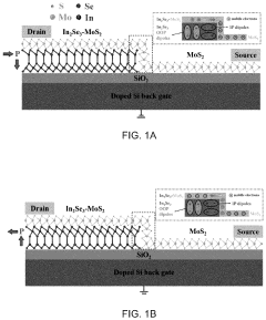
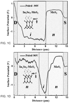
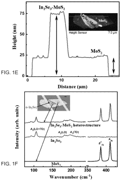
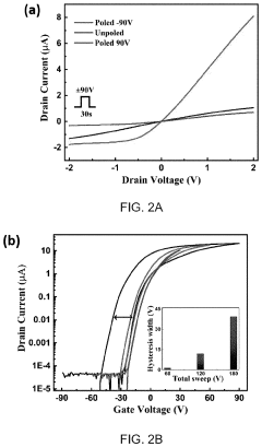
- A heterostructure system comprising a dielectric substrate, a two-dimensional ferroelectric material, and a two-dimensional semiconductor material with a polarization actuation mechanism, where the ferroelectric material is attached to the semiconductor by van der Waals forces, allowing for non-volatile polarization actuation through electrical or optical means, thereby modulating charge concentration and conductivity.
Semiconductor heterostructure and method of fabrication thereof
PatentInactiveUS9472627B2
Innovation
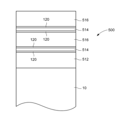
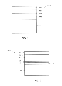
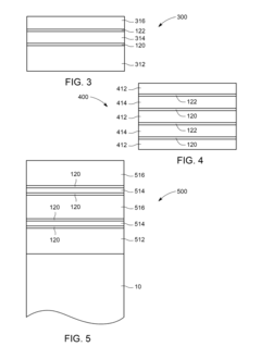
- Incorporating an intermediate semiconductor layer with an understoichiometric property (III)x>1(V)x<1, where x is less than 2, to minimize or eliminate excess antimony on the growth surface, reducing exchange with incoming arsenic atoms and enhancing the structural integrity and interface quality of the heterostructure.
Materials Science Advancements for Heterostructures
Recent advancements in materials science have revolutionized the field of semiconductor heterostructures, enabling unprecedented control over electronic and optical properties at the nanoscale. The development of novel deposition techniques, including molecular beam epitaxy (MBE) and metal-organic chemical vapor deposition (MOCVD), has allowed for atomic-level precision in creating layered structures with sharp interfaces between different semiconductor materials.
The emergence of two-dimensional materials represents a significant breakthrough in heterostructure design. Graphene, transition metal dichalcogenides (TMDs), and hexagonal boron nitride (h-BN) can be stacked with atomic precision to create van der Waals heterostructures with unique properties not achievable in traditional semiconductor systems. These materials exhibit exceptional carrier mobility, tunable bandgaps, and strong light-matter interactions, making them promising candidates for next-generation electronic and optoelectronic devices.
Strain engineering has emerged as a powerful approach to modifying the electronic properties of semiconductor heterostructures. By intentionally introducing strain through lattice mismatch or external mechanical forces, researchers can tune bandgaps, enhance carrier mobility, and even induce phase transitions in certain materials. This technique has proven particularly effective in group IV semiconductors and III-V compounds, enabling the development of high-performance electronic devices.
Advanced characterization techniques have been instrumental in understanding and optimizing heterostructure properties. High-resolution transmission electron microscopy (HRTEM), scanning tunneling microscopy (STM), and angle-resolved photoemission spectroscopy (ARPES) provide atomic-scale insights into interface quality, defect formation, and electronic band structure. These tools have accelerated the development cycle for new heterostructure designs.
The integration of novel materials with traditional semiconductors represents another frontier in heterostructure engineering. Hybrid structures combining III-V semiconductors with silicon, or integrating functional oxides with conventional semiconductors, offer pathways to devices with enhanced functionality. These heterogeneous integration approaches are overcoming fundamental limitations of individual material systems.
Computational materials science has become increasingly important in predicting and designing optimal heterostructure configurations. Density functional theory (DFT) calculations, molecular dynamics simulations, and machine learning approaches now enable researchers to screen thousands of potential material combinations before experimental validation, significantly accelerating the discovery of novel heterostructures with tailored properties.
Quantum Effects and Novel Properties
Semiconductor heterostructures exhibit remarkable quantum effects that fundamentally transform their electronic and optical properties. At the nanoscale, quantum confinement emerges as electrons become restricted in one or more dimensions, leading to discrete energy levels rather than continuous bands. This quantization dramatically alters carrier behavior, enabling novel device functionalities impossible in bulk materials. The quantum well, where carriers are confined in one dimension between barrier layers, represents the foundational heterostructure demonstrating these effects.
Quantum tunneling constitutes another critical phenomenon in heterostructures, allowing carriers to penetrate barriers they could not surmount classically. This effect enables resonant tunneling diodes, quantum cascade lasers, and tunneling field-effect transistors that exploit coherent transport mechanisms. The tunneling probability's exponential dependence on barrier thickness provides exceptional control over device characteristics through precise epitaxial growth techniques.
Band engineering in heterostructures permits manipulation of quantum states to achieve desired electronic properties. By carefully designing layer compositions and thicknesses, researchers can create artificial band structures with tailored density of states, effective masses, and mobility characteristics. This capability has revolutionized high-electron-mobility transistors (HEMTs) and modulation-doped structures where spatial separation of carriers from their parent dopants dramatically reduces scattering.
Quantum interference effects emerge in sophisticated heterostructures, particularly in systems with multiple quantum wells or superlattices. These interference phenomena can be harnessed for quantum information processing and novel optoelectronic devices. The coherent superposition of quantum states enables quantum bits (qubits) with potential applications in quantum computing architectures based on semiconductor platforms.
Topological properties represent the frontier of heterostructure quantum effects, where interface states exhibit remarkable robustness against perturbations. These topologically protected states arise from band inversions at heterojunctions between materials with different band topologies. Recent advances in topological insulators and Weyl semimetals implemented in heterostructure form demonstrate potential for dissipationless transport channels and novel spintronic devices.
The exploitation of spin-orbit coupling in heterostructures has opened pathways to spin-based electronics without ferromagnetic materials. The Rashba effect, particularly pronounced at asymmetric interfaces, enables electric-field control of spin states—a crucial capability for future spin-logic devices and quantum computation schemes utilizing spin qubits.
Unlock deeper insights with PatSnap Eureka Quick Research — get a full tech report to explore trends and direct your research. Try now!
Generate Your Research Report Instantly with AI Agent
Supercharge your innovation with PatSnap Eureka AI Agent Platform!
