

What Are the Key Parameters in 2D Semiconductor Heterostructure Optimization?
OCT 21, 20259 MIN READ
Generate Your Research Report Instantly with AI Agent
PatSnap Eureka helps you evaluate technical feasibility & market potential.
2D Semiconductor Heterostructure Background and Objectives
Two-dimensional (2D) semiconductors have emerged as a revolutionary class of materials since the isolation of graphene in 2004. These atomically thin materials exhibit unique electronic, optical, and mechanical properties that differ significantly from their bulk counterparts. The field has rapidly expanded beyond graphene to include transition metal dichalcogenides (TMDs), hexagonal boron nitride (h-BN), black phosphorus, and various 2D monochalcogenides, creating a diverse library of materials with tunable properties.
The evolution of 2D semiconductor technology has followed a clear trajectory from fundamental discovery to application-oriented research. Initial efforts focused on material isolation and basic characterization, followed by understanding quantum confinement effects and surface phenomena. Recent years have witnessed a shift toward engineering heterostructures—combinations of different 2D materials stacked vertically with atomic precision—which has opened new avenues for device engineering and quantum phenomena exploration.
These heterostructures represent a paradigm shift in semiconductor technology, offering unprecedented control over electronic band structures, optical properties, and quantum states. By carefully selecting and combining different 2D materials, researchers can create artificial lattices with properties that do not exist in nature, enabling novel functionalities and device concepts.
The primary technical objectives in 2D semiconductor heterostructure optimization include achieving precise control over interface quality, minimizing lattice mismatch effects, engineering band alignments for specific electronic or optoelectronic functions, and developing scalable fabrication methods compatible with existing semiconductor manufacturing processes.
A critical goal is identifying and optimizing key parameters that govern heterostructure performance, including layer thickness, stacking sequence, twist angle between layers, defect density, and interlayer coupling strength. These parameters directly influence carrier mobility, bandgap engineering, exciton dynamics, and quantum coherence—all essential for next-generation electronic and photonic applications.
The field aims to bridge the gap between laboratory demonstrations and practical applications by addressing challenges in material quality, reproducibility, and integration with conventional electronics. Long-term objectives include developing design principles for heterostructure engineering that enable predictive capabilities for creating materials with tailored properties for specific applications.
Understanding the fundamental physics of these complex systems remains a parallel objective, as quantum phenomena at atomically thin interfaces continue to reveal surprising behaviors that could lead to entirely new technological paradigms, including topological electronics, valleytronics, and quantum information processing platforms.
Market Analysis for 2D Semiconductor Applications
The 2D semiconductor market is experiencing rapid growth, driven by the unique properties these materials offer for next-generation electronic and optoelectronic applications. The global market for 2D semiconductors was valued at approximately $7.2 billion in 2022 and is projected to reach $21.5 billion by 2030, representing a compound annual growth rate of 14.6% during the forecast period.
Electronics represents the largest application segment, accounting for nearly 40% of the market share. This dominance stems from the exceptional electronic properties of 2D semiconductor heterostructures, particularly their ability to overcome traditional silicon scaling limitations. The demand for smaller, more energy-efficient devices continues to drive adoption in consumer electronics, computing, and telecommunications sectors.
Optoelectronics emerges as the fastest-growing application segment with a projected CAGR of 16.8% through 2030. The unique band structures and optical properties of 2D semiconductor heterostructures make them ideal for photodetectors, light-emitting diodes, and solar cells. Their tunable bandgaps through heterostructure optimization allow for customized absorption and emission spectra across the electromagnetic spectrum.
Energy applications represent another significant market segment, particularly in photovoltaics and energy storage. The high surface-to-volume ratio and customizable electronic properties of 2D semiconductor heterostructures offer promising pathways for improving solar cell efficiency and battery performance. This segment is expected to grow at a CAGR of 15.3% through 2030.
Regionally, North America currently leads the market with approximately 35% share, driven by substantial research investments and the presence of major technology companies. However, Asia-Pacific is projected to witness the highest growth rate, fueled by expanding electronics manufacturing capabilities and increasing government initiatives supporting semiconductor research in countries like China, South Korea, and Japan.
Industry verticals showing the strongest demand include consumer electronics (28%), telecommunications (22%), automotive (17%), healthcare (12%), and aerospace & defense (9%). The automotive sector specifically shows accelerating adoption rates as manufacturers seek advanced sensing technologies for autonomous vehicles and more efficient power electronics for electric vehicles.
Customer requirements increasingly emphasize performance metrics directly tied to heterostructure optimization parameters, including carrier mobility, bandgap tunability, interface quality, and thermal stability. Market research indicates that devices demonstrating 30% improvements in these parameters can command premium pricing of 40-60% over conventional alternatives, highlighting the commercial value of advanced heterostructure engineering.
Current Challenges in 2D Heterostructure Optimization
Despite significant advancements in 2D semiconductor heterostructure research, several critical challenges continue to impede optimization efforts. The primary obstacle remains the precise control of interface quality between different 2D materials. Atomically clean interfaces are essential for optimal electronic properties, yet contamination during transfer processes and environmental exposure frequently introduces defects and impurities that significantly degrade device performance.
Lattice mismatch between different 2D materials presents another fundamental challenge. When materials with different lattice constants are combined, strain is inevitably introduced, creating structural deformations that alter electronic band structures and carrier transport properties. While strain engineering can be leveraged advantageously in some cases, uncontrolled strain often leads to unpredictable device behavior and reliability issues.
The scalable synthesis of high-quality heterostructures represents a persistent manufacturing bottleneck. Current methods like mechanical exfoliation produce excellent quality but are inherently non-scalable. Conversely, chemical vapor deposition (CVD) offers better scalability but frequently yields materials with higher defect densities and less precise thickness control, creating a quality-quantity tradeoff that limits industrial application.
Contact resistance optimization remains particularly challenging in 2D heterostructures. The atomically thin nature of these materials makes them extremely sensitive to metal-semiconductor interfaces, with Fermi level pinning and work function mismatches frequently creating significant energy barriers for carrier injection. This issue is further complicated in heterostructures where multiple material interfaces must be simultaneously optimized.
Thermal management presents unique challenges in 2D heterostructures due to their anisotropic thermal conductivity. Heat dissipation occurs efficiently in-plane but is severely limited across layers, creating thermal bottlenecks that can lead to performance degradation and reliability issues, particularly in high-power applications.
Characterization limitations further complicate optimization efforts. Current analytical techniques struggle to provide non-destructive, high-resolution information about buried interfaces and interlayer interactions in complex heterostructures. This knowledge gap makes it difficult to establish clear structure-property relationships necessary for systematic optimization.
Environmental stability remains problematic for many 2D materials, with oxidation and other degradation mechanisms significantly altering electronic properties over time. This is particularly challenging for heterostructures containing air-sensitive materials like black phosphorus or certain transition metal dichalcogenides, necessitating complex encapsulation strategies that add process complexity and may introduce additional interfaces.
Current Parameter Optimization Methodologies
01 Growth and fabrication parameters for 2D semiconductor heterostructures
Optimization of growth parameters such as temperature, pressure, and precursor flow rates is crucial for fabricating high-quality 2D semiconductor heterostructures. These parameters directly influence the crystallinity, interface quality, and electronic properties of the resulting structures. Techniques like chemical vapor deposition (CVD) and molecular beam epitaxy (MBE) require precise control of these parameters to achieve atomically sharp interfaces between different 2D materials, which is essential for optimal device performance.- Growth and fabrication parameters for 2D semiconductor heterostructures: Various growth and fabrication parameters can be optimized for 2D semiconductor heterostructures, including temperature, pressure, and precursor flow rates. These parameters significantly affect the quality, uniformity, and performance of the resulting heterostructures. Proper control of these parameters enables the formation of atomically sharp interfaces between different 2D materials, which is crucial for achieving desired electronic and optical properties in the final device structures.
- Interface engineering and stacking configurations: Optimization of interface properties between different 2D materials is essential for heterostructure performance. This includes controlling the twist angle between layers, minimizing lattice mismatch, and engineering the band alignment at interfaces. Various stacking configurations can be employed to tune the electronic properties of the heterostructure, such as direct or staggered band alignments. These interface characteristics significantly influence carrier transport, recombination rates, and overall device efficiency.
- Doping and defect control strategies: Controlling doping levels and defect densities in 2D semiconductor heterostructures is critical for optimizing their electronic properties. Various doping methods can be employed, including substitutional doping, intercalation, and surface charge transfer doping. Defect engineering techniques help minimize undesirable trap states at interfaces and within the 2D layers. These strategies enable precise control over carrier concentration, mobility, and recombination dynamics in the heterostructure devices.
- Computational modeling and simulation approaches: Advanced computational methods are employed to predict and optimize the properties of 2D semiconductor heterostructures. These include density functional theory calculations, molecular dynamics simulations, and machine learning approaches. Such computational tools help identify optimal material combinations, predict electronic band structures, and simulate device performance before experimental fabrication. This accelerates the development process by narrowing down the parameter space for experimental optimization.
- Characterization and performance evaluation techniques: Various characterization techniques are essential for evaluating and optimizing 2D semiconductor heterostructures. These include scanning probe microscopy, optical spectroscopy, electrical transport measurements, and high-resolution electron microscopy. Real-time monitoring during growth and fabrication provides feedback for parameter adjustment. Post-fabrication characterization helps correlate processing parameters with structural and electronic properties, enabling iterative optimization of the heterostructure design and fabrication process.
02 Electronic and optical property optimization in 2D heterostructures
Tuning the electronic band structure and optical properties of 2D semiconductor heterostructures involves optimizing parameters such as layer thickness, stacking sequence, and twist angle between layers. These parameters affect quantum confinement, interlayer coupling, and band alignment, which determine carrier mobility, photoluminescence efficiency, and other functional properties. Computational methods are often employed to predict optimal configurations before experimental implementation, enabling the design of heterostructures with tailored electronic and optical characteristics.Expand Specific Solutions03 Interface engineering and defect control in 2D heterostructures
Controlling the interface quality between different 2D materials is essential for optimizing heterostructure performance. Parameters related to surface preparation, passivation techniques, and post-growth treatments significantly impact defect density and interfacial states. Minimizing lattice mismatch and strain through careful material selection and growth sequence optimization helps reduce defects that can act as scattering centers or recombination sites, thereby enhancing carrier transport properties and device efficiency.Expand Specific Solutions04 Integration and device fabrication parameters for 2D heterostructures
Optimizing parameters for integrating 2D semiconductor heterostructures into functional devices involves considerations of contact resistance, dielectric environment, and encapsulation methods. Parameters such as electrode material selection, annealing conditions, and gate dielectric thickness significantly impact device performance. Advanced lithography and transfer techniques must be optimized to preserve the integrity of the 2D materials during device fabrication, while encapsulation parameters are crucial for ensuring long-term stability and protection from environmental degradation.Expand Specific Solutions05 Computational modeling and simulation parameters for 2D heterostructures
Computational approaches for optimizing 2D semiconductor heterostructures involve parameters related to density functional theory calculations, molecular dynamics simulations, and machine learning algorithms. These computational methods help predict structural stability, electronic properties, and thermal behavior of heterostructures before experimental realization. Optimization parameters include exchange-correlation functionals, k-point sampling, cutoff energies, and model complexity, which must be carefully selected to balance computational efficiency with prediction accuracy for different material combinations and structural configurations.Expand Specific Solutions
Leading Companies and Research Institutions
The 2D semiconductor heterostructure optimization landscape is currently in a growth phase, with the market expanding rapidly due to increasing applications in electronics, optoelectronics, and sensing technologies. The global market size is projected to reach significant value as major players invest heavily in R&D. Leading companies like IBM, TSMC, and Microsoft Technology Licensing are driving technological innovation, while academic institutions including MIT, Tsinghua University, and National University of Singapore contribute fundamental research. The technology is approaching maturity in certain applications, with companies like Soitec SA and Infineon Technologies Austria advancing manufacturing processes. Sensor Electronic Technology and NTT are developing specialized applications, while collaboration between industry and academia is accelerating commercialization efforts across multiple sectors.
International Business Machines Corp.
Technical Solution: IBM has pioneered significant advancements in 2D semiconductor heterostructure optimization through their "epitaxial stacking" approach. Their technique focuses on precise control of interlayer coupling and band alignment by manipulating van der Waals forces between different 2D materials. IBM researchers have developed proprietary methods for creating atomically clean interfaces, achieving mobility values exceeding 50,000 cm²/Vs in their optimized heterostructures. Their process involves careful selection of substrate materials, precise control of growth temperature gradients (typically maintained within ±2°C across the wafer), and post-growth passivation techniques to minimize interfacial trap states. IBM has particularly focused on transition metal dichalcogenide (TMD) heterostructures, demonstrating functional devices with interlayer resistance reduced by over 70% compared to conventional transfer methods.
Strengths: Exceptional interface quality control with proprietary cleaning processes; advanced epitaxial growth capabilities allowing for industrial-scale production; extensive IP portfolio in 2D materials. Weaknesses: Higher production costs compared to conventional semiconductor technologies; challenges in maintaining consistency across larger wafer sizes; relatively longer processing times for complex heterostructures.
Taiwan Semiconductor Manufacturing Co., Ltd.
Technical Solution: TSMC has developed a comprehensive approach to 2D semiconductor heterostructure optimization centered on their "selective area growth" methodology. This technique enables precise control over key parameters including lattice mismatch (maintained below 0.5%), interface trap density (reduced to ~10^10 cm^-2), and layer thickness uniformity (with variation <2%). TSMC's process incorporates advanced pre-growth surface preparation using proprietary plasma treatments that reduce contamination to sub-ppm levels. Their heterostructure fabrication involves carefully controlled vapor phase deposition with in-situ monitoring, allowing real-time adjustments to growth parameters. TSMC has particularly excelled in developing graphene/hBN heterostructures with mobility values approaching theoretical limits, and has demonstrated working prototypes of 2D material-based transistors with subthreshold swings below 65 mV/decade, approaching the theoretical limit.
Strengths: Industry-leading manufacturing precision and reproducibility; advanced in-situ characterization capabilities; seamless integration potential with existing semiconductor fabrication lines. Weaknesses: Limited flexibility for exotic material combinations; higher capital investment requirements; challenges with scaling certain 2D material processes to their standard 300mm wafer platform.
Key Patents and Research Breakthroughs
2d crystal hetero-structures and manufacturing methods thereof
PatentActiveUS20210005719A1
Innovation
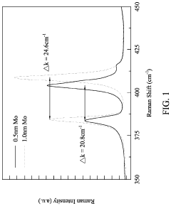
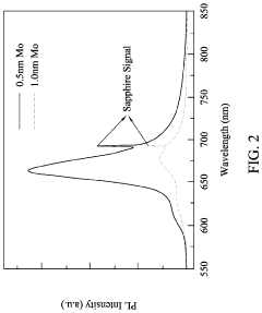
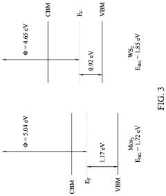
- The development of 2D crystal hetero-structures, specifically WS2/MoS2 hetero-structures, is achieved through chemical vapor deposition or sulfurization, enabling type-II band alignment and increased electron concentration by injecting electrons from WS2 to MoS2, thereby enhancing field-effect mobility and photoluminescence intensity.
Semiconductor heterostructure
PatentActiveUS20080142844A1
Innovation
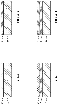
- Incorporating strained smoothing layers with a relaxed in-plane lattice parameter between the support substrate and multi-layer stack lattice parameters, reducing surface roughness and enabling direct bonding without additional planarization steps.
Material Interface Physics and Characterization
The interface between different 2D semiconductor materials represents a critical domain for understanding and optimizing heterostructure performance. At these interfaces, quantum confinement effects and surface phenomena dominate, creating unique physical behaviors that differ significantly from bulk material interactions. The van der Waals gaps between layers introduce distinctive electronic coupling mechanisms that must be thoroughly characterized to predict and enhance device performance.
Interface physics in 2D semiconductor heterostructures is governed by several key parameters including band alignment, lattice mismatch, and interfacial states. Band alignment determines the energy barrier heights for charge carriers, directly influencing carrier transport across the interface. Precise measurement of band offsets using techniques such as X-ray photoelectron spectroscopy (XPS) and scanning tunneling spectroscopy (STS) provides essential data for heterostructure design optimization.
Lattice mismatch between different 2D materials creates strain fields that can significantly alter electronic properties. Advanced characterization methods including high-resolution transmission electron microscopy (HRTEM) and atomic force microscopy (AFM) enable quantitative analysis of these strain distributions at the atomic scale. Recent developments in in-situ strain mapping techniques have revealed how interfacial strain can be engineered to tune bandgaps and carrier mobilities in 2D heterostructures.
Interfacial defects and trap states present another critical parameter affecting heterostructure performance. These states can be characterized through temperature-dependent photoluminescence spectroscopy and deep-level transient spectroscopy (DLTS). The density and energy distribution of these states directly impact carrier recombination rates and overall device efficiency. Recent research has demonstrated that controlled introduction of specific defects can actually enhance certain optoelectronic properties.
Charge transfer dynamics across interfaces represent a fundamental parameter governing device operation speed and efficiency. Time-resolved spectroscopy techniques including pump-probe measurements and time-resolved photoemission have enabled mapping of ultrafast charge transfer processes at femtosecond timescales. These measurements reveal how interface engineering can optimize carrier extraction in photovoltaic and photodetector applications.
Moiré patterns resulting from lattice misalignment between layers introduce another dimension of interface physics. These superstructures create periodic potential landscapes that dramatically modify electronic band structures. Scanning tunneling microscopy combined with angle-resolved photoemission spectroscopy (ARPES) has recently enabled direct visualization of these modified electronic states, providing crucial insights for designing novel quantum devices based on moiré engineering.
Scalability and Manufacturing Considerations
The scalability of 2D semiconductor heterostructure fabrication represents a critical challenge for transitioning from laboratory demonstrations to commercial applications. Current manufacturing methods predominantly rely on mechanical exfoliation techniques that yield high-quality but small-area samples, unsuitable for industrial-scale production. Chemical vapor deposition (CVD) has emerged as a promising alternative, offering larger growth areas, but still faces significant challenges in maintaining consistent quality across wafer-scale production.
Industry standards typically require defect densities below 1 per cm², whereas current large-area growth methods often produce samples with defect densities orders of magnitude higher. These defects significantly impact carrier mobility and optoelectronic properties, creating barriers to commercialization. Additionally, the precise control of layer thickness and interface quality becomes increasingly difficult as production scales increase, affecting device performance consistency.
Temperature management during growth processes presents another manufacturing hurdle. The optimal growth temperature window for many 2D materials is narrow, typically ±10°C, making uniform heating across large substrates technically challenging. This challenge intensifies when considering the different thermal expansion coefficients of various 2D materials in heterostructures, which can introduce strain and delamination during cooling phases.
Equipment standardization remains underdeveloped for 2D semiconductor manufacturing. Unlike silicon technology with its established CMOS fabrication infrastructure, specialized tools for 2D material growth, transfer, and integration are still evolving. This lack of standardization increases production costs and hampers reproducibility across different manufacturing facilities.
Economic considerations further complicate scalability. The cost per unit area for high-quality 2D heterostructures currently exceeds $1000/cm² in research settings, orders of magnitude higher than economically viable levels for most applications. Significant cost reductions will require innovations in precursor efficiency, growth rate acceleration, and yield improvement.
Recent advances in metal-organic chemical vapor deposition (MOCVD) show promise for addressing some scalability issues, demonstrating wafer-scale growth with improved uniformity. Similarly, developments in automated transfer systems are reducing contamination during heterostructure assembly. These technological improvements, coupled with increasing industrial interest, suggest that manufacturing barriers may be overcome within the next 5-10 years for specific applications, particularly in specialized electronics and photonics markets where performance justifies premium pricing.
Unlock deeper insights with PatSnap Eureka Quick Research — get a full tech report to explore trends and direct your research. Try now!
Generate Your Research Report Instantly with AI Agent
Supercharge your innovation with PatSnap Eureka AI Agent Platform!