Design Strategies for 2D Semiconductor Heterostructures in Electronics
OCT 21, 20259 MIN READ
Generate Your Research Report Instantly with AI Agent
Patsnap Eureka helps you evaluate technical feasibility & market potential.
2D Semiconductor Evolution and Design Objectives
Two-dimensional (2D) semiconductors have emerged as a revolutionary class of materials since the isolation of graphene in 2004. Unlike their bulk counterparts, these atomically thin materials exhibit unique electronic, optical, and mechanical properties that arise from quantum confinement effects and reduced dimensionality. The evolution of 2D semiconductors has progressed from graphene to transition metal dichalcogenides (TMDs) such as MoS2 and WSe2, to more complex materials including black phosphorus, hexagonal boron nitride (h-BN), and MXenes.
The technological trajectory of 2D semiconductors has been marked by significant milestones. Initially, research focused on fundamental property characterization, followed by the development of fabrication techniques for high-quality monolayers. Subsequently, attention shifted toward creating heterostructures—artificial materials constructed by stacking different 2D layers. These heterostructures represent a paradigm shift in semiconductor design, offering unprecedented control over electronic properties through van der Waals interactions between layers.
Current research trends indicate a growing emphasis on precision engineering of these heterostructures. The ability to manipulate band alignments, create quantum wells, and induce novel phenomena such as interlayer excitons has opened new avenues for device applications. The field is now moving toward deterministic assembly techniques, including automated pick-and-place methods and controlled growth processes that enable atomic-level precision in heterostructure formation.
The primary technical objectives in 2D semiconductor heterostructure design center around several key challenges. First is the development of scalable fabrication methods that maintain atomic precision while being compatible with existing semiconductor manufacturing infrastructure. Second is the engineering of interfaces between different 2D materials to minimize defects and optimize charge transfer. Third is the creation of novel heterostructure architectures that exploit quantum phenomena for enhanced functionality.
Looking forward, the field aims to achieve deterministic control over electronic properties through strategic layer combinations and precise twist angle engineering. The concept of "twistronics"—manipulating electronic properties by controlling the relative rotation between layers—represents a frontier with immense potential for creating designer electronic states. Additionally, researchers are pursuing integration strategies that combine 2D heterostructures with conventional semiconductors to leverage the advantages of both material systems.
The ultimate goal is to develop design principles that enable the systematic creation of 2D semiconductor heterostructures with tailored properties for specific applications, ranging from ultra-efficient electronics to quantum information processing platforms. This requires a multidisciplinary approach combining materials science, quantum physics, and electrical engineering to translate fundamental understanding into practical device architectures.
Market Analysis for 2D Heterostructure Applications
The global market for 2D semiconductor heterostructures is experiencing rapid growth, driven by increasing demand for miniaturized electronic components with enhanced performance capabilities. Current market valuations indicate that the 2D materials sector is expanding at a compound annual growth rate of approximately 19% between 2023 and 2030, with heterostructure applications representing a significant portion of this growth trajectory.
Consumer electronics remains the dominant application sector, accounting for nearly 40% of the current market share. This is primarily due to the integration of 2D heterostructures in next-generation display technologies, flexible electronics, and high-performance computing devices. The unique properties of these materials, including atomic thinness, tunable bandgaps, and superior carrier mobility, make them particularly valuable for manufacturers seeking competitive advantages in device performance and form factor.
The telecommunications sector represents the fastest-growing market segment, with an estimated growth rate exceeding 25% annually. This acceleration is largely attributed to the deployment of 5G and future 6G networks, where 2D heterostructure-based components offer significant advantages in signal processing, RF filtering, and energy efficiency. Major telecommunications equipment providers have increased their R&D investments in this technology by over 30% in the past three years.
Healthcare and biomedical applications are emerging as promising new markets, particularly for biosensing and diagnostic devices. The exceptional sensitivity of 2D heterostructures to molecular interactions makes them ideal for developing next-generation medical sensors. Market analysts project this segment to grow from a relatively small base to represent approximately 15% of the total market by 2028.
Regional market analysis reveals that East Asia currently dominates manufacturing capacity, with South Korea, Japan, and China collectively accounting for over 60% of production. However, significant investments in North America and Europe, particularly through government-funded initiatives like the EU Graphene Flagship and the US CHIPS Act, are expected to redistribute market share over the next decade.
Supply chain considerations remain a critical factor affecting market growth. The specialized production requirements for high-quality 2D materials and heterostructures have created bottlenecks that limit widespread commercial adoption. Industry consortia are actively working to standardize production methods and quality control protocols to address these challenges.
Customer adoption patterns indicate a transition from research-oriented applications to commercial products, with early adopters primarily in premium consumer electronics and specialized industrial applications. Mass market penetration is expected to accelerate after 2025, when production scaling and cost reductions reach critical thresholds that enable broader implementation across multiple industries.
Current Challenges in 2D Semiconductor Integration
Despite significant advancements in 2D semiconductor technology, several critical challenges persist in the integration of these materials into practical electronic devices. The atomically thin nature of 2D materials, while offering unique electronic properties, creates substantial difficulties in maintaining structural integrity during fabrication processes. Conventional semiconductor manufacturing techniques often damage these delicate structures, necessitating the development of specialized handling protocols.
Interface engineering represents one of the most significant hurdles in 2D semiconductor integration. When creating heterostructures, the formation of clean interfaces between different 2D materials is crucial for optimal electronic performance. Contamination, lattice mismatches, and trapped impurities at these interfaces can dramatically alter carrier transport properties, leading to degraded device performance. Current transfer methods, including mechanical exfoliation and direct growth techniques, still struggle to consistently produce pristine interfaces at scale.
Contact resistance remains a persistent challenge that limits the performance of 2D semiconductor devices. The formation of low-resistance electrical contacts to 2D materials is complicated by Fermi level pinning, work function mismatches, and the formation of Schottky barriers. These issues are particularly pronounced in transition metal dichalcogenides (TMDs) and other emerging 2D semiconductors, where contact resistance can dominate overall device resistance.
Scalable manufacturing presents another significant obstacle. While laboratory demonstrations have shown impressive results with manually assembled heterostructures, transitioning to industrial-scale production requires consistent growth methods that can produce uniform, large-area 2D materials with controlled thickness and minimal defects. Current chemical vapor deposition (CVD) and molecular beam epitaxy (MBE) techniques still face limitations in achieving this level of control across large substrates.
Environmental stability poses additional integration challenges. Many 2D semiconductors exhibit sensitivity to oxygen, moisture, and other atmospheric components, leading to performance degradation over time. Effective encapsulation strategies are needed to protect these materials without compromising their electronic properties or adding excessive complexity to device fabrication.
The lack of standardized characterization methods further complicates integration efforts. Unlike traditional semiconductors, 2D materials require specialized techniques to accurately assess layer number, defect density, and electronic properties. This makes quality control and process optimization particularly challenging, especially when working with heterostructures composed of multiple 2D materials with different physical properties.
Contemporary Fabrication Approaches
01 Fabrication methods for 2D semiconductor heterostructures
Various techniques are employed to fabricate 2D semiconductor heterostructures, including molecular beam epitaxy, chemical vapor deposition, and mechanical exfoliation followed by stacking. These methods allow for precise control over layer thickness, composition, and interface quality, which are crucial for achieving desired electronic and optical properties in the resulting heterostructures. The fabrication processes often involve careful control of growth parameters such as temperature, pressure, and precursor flow rates to ensure high-quality interfaces between different 2D materials.- Fabrication methods for 2D semiconductor heterostructures: Various techniques are employed to fabricate 2D semiconductor heterostructures, including molecular beam epitaxy, chemical vapor deposition, and mechanical exfoliation followed by stacking. These methods allow for precise control over layer thickness, composition, and interface quality, which are crucial for achieving desired electronic and optical properties in the resulting heterostructures. The fabrication processes often involve careful control of growth parameters such as temperature, pressure, and precursor flow rates to ensure high-quality interfaces between different 2D materials.
- Transition metal dichalcogenide-based heterostructures: Transition metal dichalcogenides (TMDs) such as MoS2, WS2, MoSe2, and WSe2 are widely used in 2D semiconductor heterostructures due to their tunable bandgaps and strong light-matter interactions. When these materials are combined in vertical or lateral heterostructures, they exhibit unique electronic properties including type-I, type-II, or type-III band alignments. These heterostructures show promise for applications in optoelectronics, photovoltaics, and photodetectors due to efficient charge separation and transfer across interfaces.
- Graphene-based 2D semiconductor heterostructures: Graphene serves as an excellent component in 2D semiconductor heterostructures due to its high carrier mobility and mechanical flexibility. When combined with other 2D materials like hexagonal boron nitride (h-BN) or transition metal dichalcogenides, graphene-based heterostructures demonstrate enhanced electrical conductivity, optical transparency, and mechanical strength. These structures are particularly valuable for applications in transparent electrodes, flexible electronics, and high-frequency transistors where the unique properties of graphene complement those of other 2D semiconductors.
- Optical and electronic properties of 2D semiconductor heterostructures: 2D semiconductor heterostructures exhibit distinctive optical and electronic properties arising from quantum confinement effects and interlayer interactions. These include tunable bandgaps, strong exciton binding energies, valley-selective optical transitions, and efficient charge transfer across interfaces. By engineering the stacking sequence, twist angle, and layer composition, researchers can tailor these properties for specific applications. The ability to manipulate these characteristics makes 2D heterostructures promising for next-generation optoelectronic devices, including light-emitting diodes, photodetectors, and photovoltaic cells.
- Applications of 2D semiconductor heterostructures in devices: 2D semiconductor heterostructures are being integrated into various electronic and optoelectronic devices, leveraging their unique properties. These applications include field-effect transistors with high on/off ratios and mobility, photodetectors with broadband response and high sensitivity, light-emitting diodes with tunable emission wavelengths, and sensors with exceptional sensitivity to environmental changes. The atomically thin nature of these materials also enables their integration into flexible and transparent electronics, opening new possibilities for wearable technology and smart displays.
02 Transition metal dichalcogenide-based heterostructures
Transition metal dichalcogenides (TMDs) such as MoS2, WS2, and WSe2 are widely used in 2D semiconductor heterostructures due to their tunable bandgaps and strong light-matter interactions. When combined in vertical or lateral heterostructures, these materials exhibit unique electronic properties including type-I, type-II, or type-III band alignments. These heterostructures show enhanced photoluminescence, improved carrier mobility, and efficient charge separation, making them promising for applications in optoelectronics, photovoltaics, and photodetectors.Expand Specific Solutions03 Graphene-based 2D semiconductor heterostructures
Graphene serves as an excellent platform for creating 2D semiconductor heterostructures due to its high conductivity and mechanical flexibility. When combined with other 2D materials like hexagonal boron nitride (h-BN) or transition metal dichalcogenides, graphene-based heterostructures exhibit enhanced electrical properties, improved thermal management, and unique quantum phenomena. These heterostructures can be engineered to create high-mobility transistors, efficient photodetectors, and novel quantum electronic devices with tunable properties.Expand Specific Solutions04 Optical and electronic properties of 2D semiconductor heterostructures
2D semiconductor heterostructures exhibit distinctive optical and electronic properties that can be tailored through material selection and structural design. These include direct-to-indirect bandgap transitions, exciton formation with high binding energies, valley-selective optical excitation, and quantum confinement effects. The atomically thin nature of these materials leads to reduced dielectric screening and enhanced coulomb interactions, resulting in strong light-matter coupling and unique optoelectronic behavior that can be exploited for novel device applications.Expand Specific Solutions05 Applications of 2D semiconductor heterostructures
2D semiconductor heterostructures find applications across multiple technological domains. They are used in high-performance field-effect transistors with excellent on/off ratios and low power consumption, photodetectors with broadband response and high sensitivity, light-emitting devices with tunable emission wavelengths, and energy harvesting systems including photovoltaic cells. Additionally, these heterostructures show promise for quantum computing applications, sensors, and flexible electronics due to their unique combination of electrical, optical, and mechanical properties.Expand Specific Solutions
Leading Companies and Research Institutions
The 2D semiconductor heterostructures market is currently in a growth phase, with an estimated market size of $500-700 million and projected annual growth of 25-30%. The technology is transitioning from research to commercialization, with varying maturity levels across applications. Leading players include established semiconductor manufacturers like TSMC and Micron Technology, who are leveraging their fabrication expertise, alongside specialized companies like Cambridge GaN Devices and Innoscience focusing on GaN-based solutions. Academic institutions such as MIT, Dresden University of Technology, and Chinese universities are driving fundamental research, while Fraunhofer-Gesellschaft and NaMLab bridge the research-industry gap. GLOBALFOUNDRIES and Analog Devices are advancing integration capabilities, positioning themselves for the anticipated expansion in electronics applications requiring high performance and energy efficiency.
Taiwan Semiconductor Manufacturing Co., Ltd.
Technical Solution: TSMC has developed advanced integration strategies for 2D semiconductor heterostructures focusing on industrial scalability. Their approach combines chemical vapor deposition (CVD) growth techniques with their mature semiconductor fabrication infrastructure to enable wafer-scale production of 2D material-based devices. TSMC's technology utilizes selective-area growth methods to precisely position different 2D materials on silicon substrates, creating lateral and vertical heterostructures with controlled interfaces. Their process incorporates specialized transfer techniques and surface preparation protocols to minimize contamination and defects at material boundaries. TSMC has successfully demonstrated integration of 2D materials like MoS2 and WSe2 with conventional CMOS technology, enabling hybrid devices that leverage the unique properties of 2D semiconductors while maintaining compatibility with existing manufacturing processes. Their heterostructure design strategy emphasizes reproducibility and yield optimization through careful control of growth parameters and post-processing treatments.
Strengths: Unparalleled manufacturing infrastructure for scaling 2D semiconductor technologies; established quality control systems; ability to integrate with conventional silicon technology. Weaknesses: Less flexibility in custom heterostructure designs compared to research institutions; challenges in achieving the same material quality as mechanical exfoliation methods; higher implementation costs.
SOITEC SA
Technical Solution: SOITEC has developed a specialized Smart Cut™ technology adapted for 2D semiconductor heterostructure fabrication. This proprietary process enables the transfer of ultra-thin crystalline layers of various 2D materials onto engineered substrates with precise thickness control down to the nanometer scale. For 2D semiconductor applications, SOITEC has refined their technology to create complex multi-material stacks with atomically sharp interfaces. Their approach involves hydrogen implantation to define cleavage planes, followed by wafer bonding and controlled splitting to transfer 2D material layers. SOITEC has extended this technology to incorporate strain engineering in 2D heterostructures, allowing for band structure modification and enhanced carrier mobility. Their process enables the creation of large-area 2D semiconductor heterostructures with consistent properties across the entire wafer, addressing one of the key challenges in 2D materials commercialization. SOITEC's heterostructure designs incorporate buffer layers and interface engineering to minimize lattice mismatch effects and reduce defect densities.
Strengths: Industry-leading expertise in layer transfer technologies; ability to produce large-area, uniform 2D heterostructures; excellent thickness control and reproducibility. Weaknesses: Limited flexibility for certain novel 2D materials; higher production costs compared to direct growth methods; challenges with materials requiring specific crystal orientations.
Key Patents and Scientific Breakthroughs
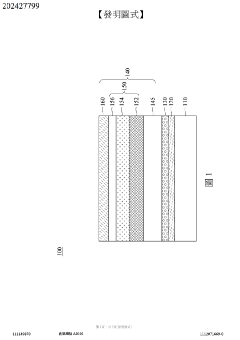
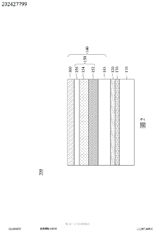
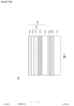
Semiconductor device
PatentActiveTW202427799A
Innovation
- A semiconductor device with a gallium nitride power device on a non-native substrate, utilizing a two-dimensional material layer and intermediate bonding layer to transfer the gallium nitride power element to a thermally conductive substrate, avoiding defects and reducing production costs.

Material Compatibility and Interface Engineering
Material compatibility and interface engineering represent critical challenges in the development of 2D semiconductor heterostructures. The atomically thin nature of 2D materials creates unique interfacial dynamics that significantly influence device performance. When integrating different 2D materials, lattice mismatch between layers can introduce strain, defects, and electronic states that alter carrier transport properties. Recent studies have demonstrated that even small lattice misalignments of 1-2% can dramatically affect band alignments and create localized states at interfaces.
Interface engineering techniques have evolved substantially to address these challenges. Chemical vapor deposition (CVD) methods now enable direct growth of lateral and vertical heterostructures with cleaner interfaces compared to mechanical transfer methods. Plasma-assisted techniques have proven effective for surface preparation, reducing contamination that typically accumulates during transfer processes. Advanced transfer methods utilizing hexagonal boron nitride (h-BN) as interfacial buffers have shown remarkable success in preserving intrinsic material properties while facilitating integration.
The van der Waals gap between 2D materials presents both challenges and opportunities. While this gap can impede efficient carrier transfer across interfaces, it also provides unique engineering possibilities not available in conventional semiconductor heterojunctions. Researchers have successfully modulated this gap through controlled pressure application, intercalation of molecules, and electrostatic gating to tune interfacial properties. These approaches have yielded heterostructures with customizable electronic characteristics.
Dangling bonds and edge effects represent another critical consideration in 2D heterostructure design. Unlike bulk materials, 2D materials exhibit heightened sensitivity to edge termination chemistry. Passivation strategies using hydrogen, fluorine, or organic molecules have demonstrated effectiveness in neutralizing reactive edge sites. Recent work has shown that controlled edge functionalization can be leveraged to engineer specific electronic properties at heterojunction interfaces.
Thermal management across dissimilar 2D materials presents additional engineering challenges. Thermal boundary resistance at interfaces can limit heat dissipation in high-performance electronic devices. Materials with complementary thermal expansion coefficients must be carefully selected to prevent delamination during thermal cycling. Emerging approaches utilizing atomic layer deposition (ALD) of ultrathin buffer layers have shown promise in improving thermal transport across interfaces while maintaining electronic integrity.
Scalability and Manufacturing Considerations
The scalability of 2D semiconductor heterostructure fabrication represents a critical challenge for transitioning from laboratory demonstrations to commercial applications. Current manufacturing methods predominantly rely on mechanical exfoliation techniques, which yield high-quality samples but suffer from inherently low throughput and poor reproducibility. Chemical vapor deposition (CVD) has emerged as a promising alternative, enabling larger-area growth of 2D materials, though challenges remain in controlling layer thickness, defect density, and interface quality across wafer-scale production.
Industry-compatible processes for heterostructure fabrication must address several key considerations. The thermal budget constraints of CMOS integration pathways require growth temperatures below 450°C for back-end-of-line compatibility. Additionally, transfer processes—often necessary when direct growth is impractical—introduce contamination risks and mechanical damage that can significantly degrade device performance. Recent advances in remote plasma-enhanced CVD and atomic layer deposition techniques show promise for addressing these thermal constraints while maintaining material quality.
Metrology and quality control present unique challenges in 2D heterostructure manufacturing. The atomically thin nature of these materials necessitates specialized characterization techniques beyond traditional semiconductor inspection methods. Raman spectroscopy, photoluminescence mapping, and atomic force microscopy must be adapted for in-line monitoring to ensure consistent heterostructure properties across large substrates.
Economic viability remains a significant hurdle, with current production costs for high-quality 2D heterostructures exceeding $1000/cm² in some cases. Scaling pathways must address both material synthesis and assembly processes to achieve cost structures compatible with commercial electronics applications. Roll-to-roll processing and direct epitaxial growth on target substrates represent promising approaches for cost reduction, though both require substantial engineering refinement.
Standardization efforts are beginning to emerge through industry consortia and research collaborations, focusing on establishing material quality metrics, process control parameters, and device performance benchmarks. These standards will be essential for supply chain development and quality assurance as the industry matures. The establishment of reliable material sources and processing equipment specifically designed for 2D materials represents another critical infrastructure need for scalable manufacturing.
Unlock deeper insights with Patsnap Eureka Quick Research — get a full tech report to explore trends and direct your research. Try now!
Generate Your Research Report Instantly with AI Agent
Supercharge your innovation with Patsnap Eureka AI Agent Platform!