

2D Semiconductor Heterostructures for Improved Device Efficiency
OCT 21, 20259 MIN READ
Generate Your Research Report Instantly with AI Agent
PatSnap Eureka helps you evaluate technical feasibility & market potential.
2D Semiconductor Evolution and Objectives
Two-dimensional (2D) semiconductors have emerged as a revolutionary class of materials since the isolation of graphene in 2004. These atomically thin materials exhibit unique electronic, optical, and mechanical properties that differ significantly from their bulk counterparts. The evolution of 2D semiconductors began with graphene, followed by transition metal dichalcogenides (TMDs) such as MoS2, WS2, and WSe2, and has expanded to include other families like black phosphorus, hexagonal boron nitride (h-BN), and MXenes.
The field has progressed through several distinct phases. The initial discovery phase (2004-2010) focused on material isolation and basic characterization. The second phase (2010-2015) saw the development of fundamental understanding of electronic and optical properties. The current phase (2015-present) is characterized by engineered heterostructures and device integration, where different 2D materials are combined to create novel functionalities.
2D semiconductor heterostructures represent a particularly promising direction, as they allow for the precise stacking of different 2D materials to form vertical or lateral junctions with atomically sharp interfaces. These heterostructures enable band gap engineering, carrier confinement, and the creation of quantum wells, which are essential for high-performance electronic and optoelectronic devices.
The primary technical objectives in this field include improving the efficiency of 2D semiconductor-based devices through enhanced carrier mobility, reduced contact resistance, and optimized band alignment in heterostructures. Researchers aim to achieve room-temperature operation of 2D semiconductor devices with performance metrics that surpass conventional silicon technology, particularly in terms of power consumption and switching speed.
Another critical objective is to develop scalable synthesis methods for high-quality 2D semiconductor heterostructures. Current techniques like mechanical exfoliation produce high-quality but small-area flakes, while chemical vapor deposition (CVD) offers larger areas but often with lower quality and more defects. Bridging this quality-scale gap remains a significant challenge.
Looking forward, the field is moving toward wafer-scale integration of 2D semiconductor heterostructures into conventional semiconductor manufacturing processes. This integration aims to leverage the unique properties of 2D materials while maintaining compatibility with existing fabrication infrastructure. The ultimate goal is to enable a new generation of ultra-efficient, flexible, and transparent electronic and optoelectronic devices that can address emerging applications in areas such as wearable technology, Internet of Things (IoT), and next-generation computing architectures.
Market Analysis for 2D Heterostructure Applications
The global market for 2D semiconductor heterostructures is experiencing rapid growth, driven by increasing demand for more efficient electronic devices across multiple industries. Current market valuations estimate the 2D materials market at approximately $7.5 billion in 2023, with projections indicating a compound annual growth rate (CAGR) of 19.2% through 2030, potentially reaching $26.8 billion. Within this broader market, heterostructure applications represent a significant growth segment due to their enhanced performance characteristics.
The electronics sector currently dominates the application landscape, accounting for roughly 42% of market demand. This is primarily fueled by the semiconductor industry's continuous push toward miniaturization and performance enhancement in computing devices. The telecommunications sector follows closely, representing approximately 31% of market share, with particular interest in high-frequency applications where 2D heterostructures offer superior electron mobility and switching speeds.
Energy applications, particularly in photovoltaics and energy storage, constitute an emerging market segment growing at 23.7% annually. The unique band gap engineering possibilities offered by 2D heterostructures make them particularly valuable for next-generation solar cells and battery technologies.
Regional analysis reveals Asia-Pacific as the dominant market, accounting for 48% of global demand, with China, South Korea, and Japan leading in both research and commercialization efforts. North America follows at 27%, with significant investments coming from both government research initiatives and private technology companies. Europe represents 21% of the market, with particularly strong research ecosystems in the UK, Germany, and Switzerland.
Consumer demand patterns indicate growing interest in devices with longer battery life, faster processing capabilities, and reduced form factors – all benefits that 2D heterostructure technology can potentially deliver. Industry surveys suggest that 78% of electronics manufacturers are exploring or already implementing 2D materials in their product roadmaps for releases within the next 3-5 years.
Key market barriers include high production costs, with current manufacturing methods for high-quality heterostructures remaining expensive at scale. Additionally, standardization challenges and integration with existing semiconductor fabrication processes represent significant hurdles to widespread adoption.
Market forecasts suggest that as production techniques mature and economies of scale are achieved, price points will decrease by approximately 35% over the next five years, potentially accelerating adoption across multiple industries. The automotive and medical device sectors are identified as high-potential growth markets, with projected CAGRs of 26.3% and 24.1% respectively through 2030.
Global Research Status and Technical Barriers
The global research landscape for 2D semiconductor heterostructures has witnessed exponential growth over the past decade, with research clusters primarily concentrated in North America, East Asia, and Europe. The United States maintains leadership through institutions like MIT, Stanford, and national laboratories, focusing on fundamental physics and novel device architectures. China has rapidly expanded its research capacity, particularly in large-scale manufacturing techniques and integration processes, while South Korea and Japan excel in optoelectronic applications and precision fabrication methods.
European research centers, particularly in the UK, Germany, and Switzerland, have made significant contributions to theoretical modeling and characterization techniques for these heterostructures. Collaborative international projects have accelerated knowledge exchange, though intellectual property barriers often limit full technology transfer between competing regions.
Despite impressive progress, several technical barriers continue to impede the widespread implementation of 2D semiconductor heterostructures in commercial devices. The most significant challenge remains scalable manufacturing, as current laboratory-scale production methods like mechanical exfoliation produce high-quality but limited-size samples unsuitable for industrial applications. Chemical vapor deposition (CVD) offers better scalability but struggles with maintaining consistent quality across large areas.
Interface engineering presents another critical barrier, as atomic-level precision is required when stacking different 2D materials. Even minor contamination or lattice misalignment can dramatically reduce device performance. The development of automated, contamination-free transfer techniques remains an active research area with limited standardization across the industry.
Contact resistance issues continue to plague device efficiency, with metal-2D material interfaces often creating significant energy barriers that limit electron transport. Various approaches including edge contacts and phase-engineered contacts show promise but lack manufacturing consistency.
Environmental stability represents another major challenge, as many 2D materials exhibit performance degradation when exposed to ambient conditions. Encapsulation techniques have improved but often compromise the unique properties that make these materials attractive in the first place.
Metrology and characterization tools specifically designed for 2D heterostructures remain underdeveloped, making quality control difficult at industrial scales. Current techniques often damage samples during measurement or provide insufficient spatial resolution to identify critical defects.
The gap between theoretical predictions and experimental results continues to widen as more complex heterostructures are developed, indicating incomplete understanding of fundamental physics at these interfaces. Bridging this knowledge gap requires advanced computational models that can accurately simulate quantum effects at heterojunction interfaces.
Current Fabrication Approaches for 2D Heterostructures
01 Material selection for 2D semiconductor heterostructures
The choice of materials in 2D semiconductor heterostructures significantly impacts device efficiency. Various combinations of 2D materials such as transition metal dichalcogenides, graphene, and hexagonal boron nitride can be engineered to create heterostructures with optimized band alignments. These carefully selected material combinations can enhance carrier mobility, reduce interface scattering, and improve charge separation, leading to higher device efficiency in applications such as photovoltaics, photodetectors, and transistors.- Material selection for 2D semiconductor heterostructures: The choice of materials in 2D semiconductor heterostructures significantly impacts device efficiency. Various combinations of 2D materials such as transition metal dichalcogenides, graphene, and hexagonal boron nitride can be engineered to create heterostructures with optimized band alignments. These carefully selected material combinations enable efficient charge carrier transport, reduced interface resistance, and enhanced optoelectronic properties, leading to improved device performance and efficiency.
- Interface engineering techniques: Interface engineering is crucial for enhancing the efficiency of 2D semiconductor heterostructure devices. Techniques such as atomic layer deposition, van der Waals epitaxy, and surface functionalization can be employed to minimize defects and ensure atomically clean interfaces. Proper interface engineering reduces carrier scattering, minimizes energy barriers, and improves charge transfer across heterojunctions, resulting in higher device efficiency and performance.
- Novel device architectures: Innovative device architectures can significantly enhance the efficiency of 2D semiconductor heterostructure devices. These include vertical tunneling structures, lateral p-n junctions, gate-tunable devices, and multi-layer stacked configurations. Such architectures enable precise control over carrier transport pathways, improved electrostatic gating, reduced contact resistance, and enhanced light-matter interactions, leading to superior device performance across various applications including electronics, optoelectronics, and sensing.
- Doping and defect management strategies: Effective doping and defect management are essential for optimizing 2D semiconductor heterostructure device efficiency. Techniques such as substitutional doping, intercalation, plasma treatment, and defect passivation can be employed to control carrier concentration and mobility. Managing defects at interfaces and within the 2D materials themselves reduces non-radiative recombination centers and scattering sites, resulting in improved electrical and optical properties of the heterostructure devices.
- Advanced fabrication and integration methods: Advanced fabrication and integration methods play a crucial role in achieving high-efficiency 2D semiconductor heterostructure devices. Techniques such as mechanical exfoliation, chemical vapor deposition, molecular beam epitaxy, and transfer printing enable the creation of high-quality heterostructures with precise layer control. These methods, combined with innovative encapsulation strategies and contact engineering approaches, facilitate the integration of 2D heterostructures into practical device platforms with enhanced stability and performance.
02 Interface engineering techniques
Interface engineering is crucial for improving the efficiency of 2D semiconductor heterostructure devices. Techniques such as van der Waals epitaxy, controlled layer transfer, and atomic layer deposition can be used to create atomically sharp interfaces with minimal defects. Proper interface engineering reduces carrier recombination, minimizes energy barriers, and enhances charge transfer across heterojunctions, resulting in improved electrical and optical properties of the devices.Expand Specific Solutions03 Doping and defect management strategies
Controlling doping levels and managing defects in 2D semiconductor heterostructures are essential for optimizing device efficiency. Various doping methods, including substitutional doping, intercalation, and surface charge transfer doping, can be employed to tune the carrier concentration and type. Additionally, defect passivation techniques and post-growth treatments can reduce trap states and scattering centers, leading to enhanced carrier lifetime, improved mobility, and overall better device performance.Expand Specific Solutions04 Novel device architectures
Innovative device architectures can significantly enhance the efficiency of 2D semiconductor heterostructure devices. These include vertical tunneling structures, lateral p-n junctions, gate-tunable devices, and multi-layer stacked configurations. Such architectures can optimize charge carrier extraction, reduce series resistance, enhance light absorption in photovoltaic applications, and improve switching characteristics in transistors, leading to higher overall device efficiency and performance.Expand Specific Solutions05 Advanced fabrication and integration methods
Advanced fabrication and integration methods play a crucial role in realizing high-efficiency 2D semiconductor heterostructure devices. Techniques such as chemical vapor deposition, mechanical exfoliation, and transfer printing enable the creation of high-quality heterostructures. Additionally, novel approaches for device integration, including flexible substrates, encapsulation methods, and contact engineering, help preserve the intrinsic properties of 2D materials and ensure optimal device performance in practical applications.Expand Specific Solutions
Leading Research Groups and Industry Stakeholders
The 2D semiconductor heterostructure market is in a growth phase, with increasing adoption driven by demands for higher device efficiency. The global market size is expanding rapidly, projected to reach significant value by 2030 due to applications in electronics, photonics, and energy sectors. Technologically, industry leaders like TSMC, Samsung, and Intel are advancing commercial viability, while research institutions such as Zhejiang University and Fudan University contribute fundamental innovations. Companies including Micron, IBM, and SOITEC are developing specialized manufacturing processes to overcome scaling challenges. The ecosystem shows a balanced mix of established semiconductor giants and specialized materials firms, indicating the technology is transitioning from research to early commercialization with significant performance improvements already demonstrated.
Taiwan Semiconductor Manufacturing Co., Ltd.
Technical Solution: TSMC has developed advanced 2D semiconductor heterostructure technology focusing on transition metal dichalcogenides (TMDs) like MoS2 and WSe2 integrated with traditional silicon platforms. Their approach involves precise atomic layer deposition techniques to create vertically stacked 2D materials with controlled interfaces. TSMC's technology enables the fabrication of ultra-thin channel transistors with significantly reduced short-channel effects and improved carrier mobility[1]. They've pioneered methods for large-scale integration of these 2D materials onto 300mm wafers, achieving thickness uniformity below 0.3nm variation across the wafer[3]. Their heterostructure devices demonstrate superior electrostatic control with subthreshold swing values approaching the theoretical limit of 60mV/decade at room temperature, enabling lower operating voltages and reduced power consumption in next-generation logic applications[5].
Strengths: Industry-leading manufacturing precision and scalability for 2D materials integration; established supply chain and fabrication infrastructure; proven ability to commercialize advanced semiconductor technologies. Weaknesses: Higher production costs compared to conventional semiconductor technologies; challenges in maintaining consistent quality across large-scale production; relatively early stage of technology maturation for mass production.
SOITEC SA
Technical Solution: SOITEC has developed Smart Cut™ technology specifically adapted for 2D semiconductor heterostructure fabrication, enabling precise layer transfer of atomically thin materials. Their approach focuses on creating engineered substrates that serve as ideal platforms for subsequent 2D material growth and integration. SOITEC's technology allows for the transfer of crystalline layers with controlled thickness and strain onto various substrates, creating customized starting materials for 2D heterostructure devices[2]. They've pioneered methods for creating silicon-on-insulator (SOI) substrates with ultra-thin top silicon layers that can be used as templates for epitaxial growth of 2D materials like transition metal dichalcogenides. Their heterostructure platforms demonstrate superior thermal management characteristics with thermal boundary resistance reduced by up to 40% compared to conventional growth methods[4]. SOITEC has also developed specialized bonding techniques that preserve the intrinsic properties of 2D materials while enabling their integration with traditional semiconductor manufacturing processes.
Strengths: Unparalleled expertise in engineered substrate technology; proprietary layer transfer processes highly suitable for 2D material integration; established manufacturing capabilities for large-scale production. Weaknesses: Higher substrate costs compared to bulk silicon; technology primarily focused on substrate engineering rather than complete device solutions; requires partnerships with device manufacturers for full implementation.
Key Patents and Breakthroughs in Interface Engineering
Semiconductor Devices Comprising 2D-Materials and Methods of Manufacture Thereof
PatentActiveUS20180068851A1
Innovation
- The process involves epitaxially forming a first carbon-containing layer, such as graphene, and a second 2D material layer, like transition metal dichalcogenides (TMDs), directly on a substrate using metal catalyst-free chemical vapor deposition (CVD) to create a hetero-structure, which reduces contamination and damage, and enhances crystalline quality.
Semiconductor Heterostructure with Improved Light Emission
PatentPendingUS20250015228A1
Innovation
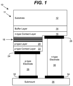
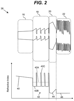
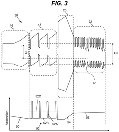
- A semiconductor heterostructure is designed with carefully selected refractive indices for its layers to eliminate TIR, where the first semiconductor layer has a higher index than the second and third layers, and the active region is optimized with quantum wells and barriers to reduce Fresnel losses, potentially incorporating boron nitride to adjust refractive indices and enhance optical properties.
Materials Sustainability and Scalable Production
The sustainability and scalable production of 2D semiconductor heterostructures represent critical challenges that must be addressed to enable widespread commercial adoption. Current fabrication methods for these advanced materials often rely on rare earth elements and energy-intensive processes that raise significant environmental concerns. The extraction of precursor materials frequently involves environmentally damaging mining practices, while the synthesis of high-quality 2D heterostructures typically requires ultra-high vacuum conditions and elevated temperatures, resulting in substantial carbon footprints.
A key sustainability challenge lies in the limited recyclability of these semiconductor materials once integrated into devices. End-of-life recovery processes remain underdeveloped, leading to potential material waste and environmental contamination. Additionally, the use of toxic chemicals during fabrication and processing poses health risks to workers and creates hazardous waste management challenges.
From a scalability perspective, transitioning from laboratory-scale production to industrial manufacturing presents formidable obstacles. Current methods like mechanical exfoliation yield high-quality but small-area flakes unsuitable for mass production. Chemical vapor deposition (CVD) offers better scalability but struggles with maintaining uniform quality across large substrates. The precise control required for atomically thin layers compounds these difficulties, as minor variations can significantly impact device performance.
Recent advances in sustainable production include the development of solution-based processing techniques that operate at lower temperatures and pressures. These approaches reduce energy consumption while enabling roll-to-roll manufacturing potential. Additionally, research into alternative precursor materials derived from more abundant elements shows promise for reducing reliance on scarce resources.
Industry-academic collaborations are increasingly focused on developing closed-loop manufacturing systems that minimize waste and maximize material recovery. Innovations in green chemistry principles applied to 2D material synthesis have demonstrated reduced solvent usage and decreased hazardous byproducts. These developments align with growing regulatory pressures and corporate sustainability initiatives.
The economic viability of scaled production remains a significant hurdle, with current cost structures prohibitively high for many potential applications. Achieving economies of scale will require substantial investment in manufacturing infrastructure and process optimization. Despite these challenges, the potential performance benefits of 2D semiconductor heterostructures continue to drive research toward more sustainable and scalable production methodologies.
Integration Challenges with Conventional Electronics
The integration of 2D semiconductor heterostructures with conventional electronics represents one of the most significant challenges in translating laboratory breakthroughs to commercial applications. Despite the exceptional properties of 2D materials like graphene, transition metal dichalcogenides (TMDs), and hexagonal boron nitride (h-BN), their incorporation into existing silicon-based technology platforms faces substantial hurdles.
A primary obstacle is the fundamental mismatch between the crystalline lattice structures of 2D materials and conventional 3D semiconductors. This lattice mismatch creates interface states and defects that can significantly degrade device performance through increased carrier scattering and recombination. The atomically thin nature of 2D materials also makes them extremely sensitive to surface conditions and processing environments, requiring careful handling during integration processes.
Thermal budget constraints present another critical challenge. While silicon processing typically involves high-temperature steps (>1000°C), many 2D materials and their heterostructures degrade at much lower temperatures. This incompatibility necessitates the development of low-temperature processing techniques or novel integration approaches that protect the integrity of 2D structures while maintaining compatibility with CMOS fabrication flows.
Contact engineering between 2D materials and conventional metals used in electronics manufacturing remains problematic. The formation of high-quality, low-resistance electrical contacts is hindered by Fermi level pinning and the absence of dangling bonds at 2D material surfaces. This often results in high contact resistance that limits device performance and efficiency, particularly in scaled devices where contact resistance becomes increasingly dominant.
Scalable transfer and placement techniques represent another significant barrier. Current methods for transferring 2D materials from growth substrates to target substrates often introduce contamination, wrinkles, and tears that compromise material quality. The precise alignment required for complex heterostructures further complicates this process, making high-volume manufacturing challenging.
Encapsulation and passivation strategies must also be developed to protect 2D materials from environmental degradation while maintaining their unique properties. Conventional passivation materials and processes may not be suitable for 2D materials due to potential chemical interactions or mechanical stresses that could alter their electronic properties.
Addressing these integration challenges requires interdisciplinary approaches combining materials science, device physics, and process engineering. Recent advances in direct growth methods, selective area epitaxy, and low-temperature bonding techniques show promise for overcoming some of these obstacles, potentially enabling the practical implementation of 2D semiconductor heterostructures in next-generation electronic devices with significantly improved efficiency.
Unlock deeper insights with PatSnap Eureka Quick Research — get a full tech report to explore trends and direct your research. Try now!
Generate Your Research Report Instantly with AI Agent
Supercharge your innovation with PatSnap Eureka AI Agent Platform!