Regulatory Considerations for 2D Semiconductor Heterostructures in Healthcare
OCT 21, 202510 MIN READ
Generate Your Research Report Instantly with AI Agent
Patsnap Eureka helps you evaluate technical feasibility & market potential.
2D Semiconductor Heterostructures Background and Healthcare Goals
Two-dimensional (2D) semiconductor heterostructures represent a revolutionary class of materials that have emerged from the discovery of graphene in 2004. These atomically thin materials, including transition metal dichalcogenides (TMDs), hexagonal boron nitride (h-BN), and phosphorene, exhibit unique electronic, optical, and mechanical properties that differ significantly from their bulk counterparts. The reduced dimensionality of these materials leads to quantum confinement effects, resulting in distinctive band structures and enhanced carrier mobility that make them particularly promising for next-generation electronic and optoelectronic applications.
The evolution of 2D semiconductor technology has progressed rapidly over the past decade, moving from fundamental research to potential commercial applications. Initial research focused primarily on graphene, but has since expanded to include a diverse array of 2D materials with semiconducting properties. The ability to stack different 2D materials to form van der Waals heterostructures has opened new avenues for designing materials with tailored properties, effectively creating "artificial solids" with unprecedented functionalities.
In the healthcare domain, 2D semiconductor heterostructures offer transformative potential across multiple applications. Their exceptional surface-to-volume ratio makes them highly sensitive to environmental changes, positioning them as ideal candidates for biosensing applications. Their biocompatibility, coupled with unique optical properties, enables advanced bioimaging techniques that can visualize cellular processes with unprecedented resolution.
The primary technical goals for 2D semiconductor heterostructures in healthcare include developing ultra-sensitive biosensors capable of detecting biomarkers at previously unattainable concentrations, creating implantable bioelectronic devices for real-time health monitoring, and engineering drug delivery systems with precise targeting capabilities. Additionally, researchers aim to harness these materials for next-generation neural interfaces that can more effectively integrate with biological tissues.
Regulatory considerations for these technologies are particularly complex due to their novel properties and potential for direct interaction with biological systems. As these materials transition from laboratory research to clinical applications, understanding the regulatory landscape becomes crucial for successful commercialization and patient safety.
The convergence of 2D semiconductor technology with healthcare applications necessitates a comprehensive regulatory framework that addresses both the unique properties of these materials and their intended medical uses. Current regulatory approaches may require adaptation to adequately assess the safety and efficacy of these novel technologies, particularly regarding biocompatibility, long-term stability in biological environments, and potential toxicological concerns.
Healthcare Market Demand for 2D Semiconductor Applications
The healthcare sector is witnessing a significant surge in demand for advanced semiconductor technologies, particularly 2D semiconductor heterostructures. This emerging market is driven by the increasing need for miniaturized, high-performance medical devices and diagnostic tools. The global medical device market, currently valued at approximately $500 billion, is projected to grow at a compound annual growth rate of 5.4% through 2028, with smart medical devices representing the fastest-growing segment.
2D semiconductor applications are particularly sought after in several key healthcare domains. In medical imaging, these materials offer enhanced sensitivity and resolution for next-generation imaging devices, addressing the $40 billion medical imaging market that demands ever-more precise diagnostic capabilities. The biosensing segment, valued at $25 billion, requires ultra-sensitive detection mechanisms for which 2D materials like graphene and molybdenum disulfide provide ideal electrical and optical properties.
Wearable health monitoring devices represent another substantial market opportunity, expected to reach $67 billion by 2025. These devices benefit from the flexibility, transparency, and low power consumption characteristics of 2D semiconductor heterostructures, enabling continuous health monitoring with minimal patient discomfort.
Implantable medical devices constitute a critical application area with stringent requirements for biocompatibility and longevity. The market for these devices exceeds $30 billion annually, with neural interfaces and smart drug delivery systems showing particular promise for 2D semiconductor integration due to their unique electrical properties and minimal footprint.
Healthcare providers are increasingly demanding precision medicine solutions, creating a $78 billion market opportunity for technologies that can facilitate personalized treatment approaches. 2D semiconductor-based diagnostic platforms offer the potential for rapid, point-of-care testing with high specificity and sensitivity.
Regional analysis reveals varying adoption rates, with North America leading in market value at 42% of global share, followed by Europe (28%) and Asia-Pacific (22%). The latter region demonstrates the fastest growth rate at 7.8% annually, driven by increasing healthcare infrastructure investments and technological adoption in China, Japan, and South Korea.
Key market constraints include cost barriers for widespread implementation, with current manufacturing processes for medical-grade 2D semiconductor devices remaining expensive. Additionally, healthcare stakeholders express concerns regarding long-term reliability and the need for comprehensive clinical validation before mainstream adoption can occur.
Current State and Regulatory Challenges of 2D Semiconductors
The global landscape of 2D semiconductor technology has witnessed remarkable growth in recent years, with significant advancements in materials science, fabrication techniques, and application development. Currently, graphene, transition metal dichalcogenides (TMDs), and hexagonal boron nitride (h-BN) represent the most extensively researched and commercially viable 2D materials. These materials have demonstrated exceptional electronic, optical, and mechanical properties that make them particularly promising for healthcare applications, including biosensing, drug delivery, and medical imaging.
Despite their potential, the integration of 2D semiconductor heterostructures into healthcare systems faces substantial regulatory challenges across different jurisdictions. In the United States, the FDA has yet to establish specific regulatory frameworks for 2D semiconductor-based medical devices, creating uncertainty for manufacturers and researchers. These technologies often fall into regulatory gray areas between traditional medical devices and novel nanomaterials, complicating the approval process.
The European Union, through its Medical Device Regulation (MDR) and In Vitro Diagnostic Regulation (IVDR), has implemented more comprehensive approaches to emerging technologies, but still lacks specific provisions for 2D semiconductor materials. This regulatory gap has resulted in inconsistent evaluation standards and prolonged approval timelines for innovative healthcare solutions utilizing these materials.
In Asia, particularly in China, Japan, and South Korea, regulatory bodies have shown greater flexibility in accommodating novel materials in medical applications, but standardization remains a significant challenge. The absence of harmonized international standards for characterizing and validating 2D semiconductor heterostructures in biological environments has hindered global market access and technology transfer.
A critical technical challenge facing regulatory bodies worldwide is the assessment of long-term biocompatibility and potential toxicity of 2D materials. Current testing protocols were primarily designed for conventional materials and may not adequately capture the unique interactions between 2D nanomaterials and biological systems. Research indicates that factors such as layer number, lateral dimensions, and surface functionalization significantly influence the biological response to these materials.
Manufacturing consistency and quality control represent additional regulatory hurdles. The properties of 2D semiconductor heterostructures are highly dependent on fabrication conditions, and slight variations can lead to significant differences in performance and safety profiles. Regulatory frameworks must address these challenges by establishing robust characterization methods and acceptance criteria specific to 2D materials.
Intellectual property considerations further complicate the regulatory landscape, with overlapping patent claims on fundamental 2D material technologies potentially restricting innovation and market access. This has led to geographic disparities in research activity and commercial development, with certain regions emerging as hubs for 2D semiconductor innovation in healthcare applications.
Current Regulatory Compliance Solutions for Medical Semiconductors
01 Fabrication methods for 2D semiconductor heterostructures
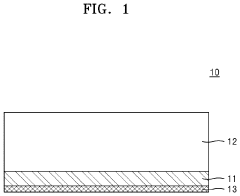
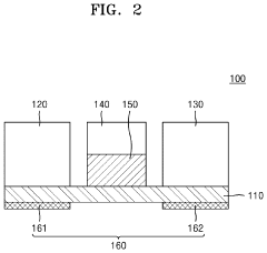
Various techniques are employed to fabricate 2D semiconductor heterostructures, including molecular beam epitaxy, chemical vapor deposition, and mechanical exfoliation followed by stacking. These methods allow for precise control over the thickness, composition, and interface quality of the heterostructures. The fabrication processes often involve careful control of growth parameters such as temperature, pressure, and precursor flow rates to achieve high-quality interfaces between different 2D materials.- Fabrication methods for 2D semiconductor heterostructures: Various techniques are employed to fabricate 2D semiconductor heterostructures, including molecular beam epitaxy, chemical vapor deposition, and mechanical exfoliation. These methods allow for precise control over the growth and stacking of atomically thin layers to create heterostructures with desired electronic and optical properties. The fabrication processes often involve careful control of temperature, pressure, and precursor materials to ensure high-quality interfaces between different 2D materials.
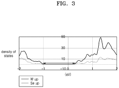
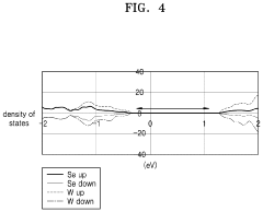
- Transition metal dichalcogenide (TMD) heterostructures: Transition metal dichalcogenide (TMD) materials such as MoS2, WS2, and WSe2 are commonly used in 2D semiconductor heterostructures due to their unique electronic and optical properties. When these materials are stacked together or combined with other 2D materials, they form heterostructures with tunable bandgaps and enhanced carrier mobility. These TMD-based heterostructures exhibit strong light-matter interactions and are promising for applications in optoelectronics, photonics, and valleytronics.
- Graphene-based 2D heterostructures: Graphene serves as an important building block in many 2D semiconductor heterostructures due to its exceptional electrical conductivity and mechanical strength. When combined with other 2D semiconductors, graphene can function as a contact electrode, carrier transport layer, or substrate. Graphene-based heterostructures often exhibit enhanced electrical properties, including improved carrier mobility and reduced contact resistance, making them suitable for high-performance electronic and optoelectronic devices.
- Optoelectronic applications of 2D semiconductor heterostructures: 2D semiconductor heterostructures are widely used in optoelectronic applications due to their unique optical properties and tunable bandgaps. These heterostructures can be engineered to create photodetectors, light-emitting diodes, solar cells, and photonic devices with enhanced performance. The atomically thin nature of these materials allows for efficient light absorption and emission, while the van der Waals interfaces between layers facilitate efficient carrier transport and separation, leading to improved device efficiency.
- Novel properties and quantum phenomena in 2D heterostructures: 2D semiconductor heterostructures exhibit unique quantum phenomena not observed in bulk materials, including quantum confinement effects, interlayer excitons, and valley-selective optical transitions. These quantum properties arise from the reduced dimensionality and the strong interactions between layers in the heterostructure. Researchers are exploring these novel properties for applications in quantum computing, spintronics, and next-generation information processing technologies. The ability to precisely control the layer composition and stacking order allows for engineering specific quantum states and phenomena.
02 Transition metal dichalcogenide (TMD) heterostructures
Heterostructures composed of different transition metal dichalcogenides (TMDs) such as MoS2, WS2, MoSe2, and WSe2 exhibit unique electronic and optical properties. These heterostructures can form type-I, type-II, or type-III band alignments, enabling applications in optoelectronics, photovoltaics, and photodetectors. The atomically sharp interfaces between different TMD layers lead to efficient charge separation and transfer, making them promising for next-generation electronic and optoelectronic devices.Expand Specific Solutions03 Graphene-based 2D heterostructures
Graphene can be combined with other 2D materials to form heterostructures with enhanced properties. These heterostructures leverage graphene's high carrier mobility and conductivity while addressing its zero bandgap limitation through integration with semiconducting 2D materials. Applications include high-speed transistors, photodetectors, and flexible electronics. The van der Waals interactions between graphene and other 2D materials allow for the creation of atomically thin devices with minimal interfacial defects.Expand Specific Solutions04 Optical and electronic properties of 2D semiconductor heterostructures
2D semiconductor heterostructures exhibit unique optical and electronic properties due to quantum confinement effects and interlayer interactions. These properties include tunable bandgaps, strong exciton binding energies, valley polarization, and layer-dependent photoluminescence. By engineering the stacking sequence and twist angle between layers, the electronic band structure can be modified, leading to phenomena such as moiré patterns and interlayer excitons that can be exploited for novel optoelectronic applications.Expand Specific Solutions05 Applications of 2D semiconductor heterostructures
2D semiconductor heterostructures find applications in various fields including electronics, optoelectronics, energy harvesting, and sensing. They can be used to create high-performance field-effect transistors, photodetectors with broadband response, efficient solar cells, and ultrasensitive sensors. The atomically thin nature of these heterostructures allows for flexible and transparent devices, while their unique electronic properties enable novel quantum technologies such as valleytronics and spintronics.Expand Specific Solutions
Key Industry Players in 2D Semiconductor Healthcare Applications
The regulatory landscape for 2D semiconductor heterostructures in healthcare is evolving within an early-to-growth market phase, with global market size projected to reach $5-7 billion by 2028. Technical maturity varies significantly across applications, with diagnostic devices advancing faster than therapeutic implementations. Leading players like Taiwan Semiconductor Manufacturing Co. and Massachusetts Institute of Technology are establishing foundational patents, while companies such as Analog Devices and Brolis Sensor Technology are developing specialized healthcare applications. Research institutions including Zhejiang University and National University of Singapore are accelerating innovation in biocompatibility and regulatory compliance frameworks. The fragmented competitive landscape suggests significant opportunity for early movers who can navigate the complex regulatory requirements spanning medical device, nanomaterial safety, and data privacy regulations.
Taiwan Semiconductor Manufacturing Co., Ltd.
Technical Solution: TSMC has developed a regulatory compliance framework for 2D semiconductor heterostructures in healthcare that leverages their extensive experience in semiconductor manufacturing quality systems. Their approach focuses on establishing rigorous process control and validation methodologies specifically adapted for the unique challenges of atomically thin materials in medical applications. TSMC has implemented specialized clean room protocols and contamination control strategies for 2D materials intended for healthcare applications, exceeding standard semiconductor industry practices to address biocompatibility concerns. Their regulatory strategy includes comprehensive material qualification procedures that evaluate both the electrical performance and biological safety aspects of 2D heterostructures, with particular attention to interface stability under physiological conditions. TSMC has established detailed documentation systems that track material sourcing, processing parameters, and quality control metrics throughout the manufacturing process, providing the traceability required by healthcare regulators. Additionally, they have developed specialized packaging solutions for 2D material-based healthcare devices that maintain material integrity while meeting biocompatibility requirements.
Strengths: Unparalleled manufacturing scale and quality control systems; extensive experience with semiconductor industry regulations that can be adapted to healthcare; strong capabilities in process consistency and reproducibility. Weaknesses: Less experience with biological testing and clinical validation compared to healthcare-focused organizations; regulatory approach may be overly focused on manufacturing aspects rather than clinical considerations.
Massachusetts Institute of Technology
Technical Solution: MIT has developed a comprehensive regulatory framework for 2D semiconductor heterostructures in healthcare applications, focusing on biocompatibility assessment protocols specifically designed for atomically thin materials. Their approach includes standardized toxicity testing methodologies for graphene, transition metal dichalcogenides (TMDs), and other 2D materials when interfaced with biological systems. MIT researchers have established a multi-tier evaluation system that addresses both acute and chronic exposure scenarios, with particular attention to the unique surface chemistry and degradation pathways of 2D materials in physiological environments. The framework incorporates real-time monitoring of material integrity and potential leaching of constituent elements when exposed to biological fluids, addressing FDA concerns about novel nanomaterials. MIT's regulatory approach also includes specialized protocols for evaluating the performance stability of 2D heterostructure-based biosensors under various sterilization procedures required for medical devices.
Strengths: Comprehensive testing protocols specifically designed for 2D materials; strong collaboration with regulatory bodies; extensive experience with biocompatibility assessment. Weaknesses: Protocols may be overly academic and challenging to implement in industrial settings; limited focus on mass-production considerations that would be necessary for widespread healthcare adoption.
Critical Patents and Innovations in Healthcare 2D Heterostructures
Heterostructure having non-volatile actuatable polarization
PatentPendingUS20240162367A1
Innovation
- A heterostructure system comprising a dielectric substrate, a two-dimensional ferroelectric material, and a two-dimensional semiconductor material with a polarization actuation mechanism, where the ferroelectric material is attached to the semiconductor by van der Waals forces, allowing for non-volatile polarization actuation through electrical or optical means, thereby modulating charge concentration and conductivity.
Semiconductor device including two dimensional material
PatentPendingUS20240113211A1
Innovation
- A semiconductor device structure is introduced that includes a two-dimensional material layer with a conductive layer and an alignment adjusting layer, which adjusts the energy-band alignment between the two-dimensional material layer and the conductive layer, using materials like RuCl3, NbS2, and WO3 to provide holes or electrons, thereby reducing contact resistance.
FDA and International Approval Pathways for Novel Medical Materials
The regulatory landscape for 2D semiconductor heterostructures in healthcare applications presents a complex matrix of approval pathways across different jurisdictions. The FDA's regulatory framework categorizes these novel materials based on their intended use, risk profile, and mechanism of action. For 2D semiconductor heterostructures, classification typically falls under either medical devices or combination products, depending on whether the primary mode of action is physical or biological.
Within the FDA structure, the Center for Devices and Radiological Health (CDRH) oversees most 2D semiconductor applications, particularly those used in diagnostic or monitoring capacities. The approval pathway generally follows either the 510(k) clearance process for devices substantially equivalent to predicate devices, or the more rigorous Premarket Approval (PMA) for novel technologies without clear predicates. For 2D materials with unique properties, De Novo classification requests have become increasingly common.
International regulatory frameworks show significant variation in their approach to novel materials. The European Union's Medical Device Regulation (MDR) and In Vitro Diagnostic Regulation (IVDR) implement a risk-based classification system with more stringent requirements for clinical evidence and post-market surveillance than previous directives. Notably, the EU places greater emphasis on the precautionary principle regarding nanomaterials, potentially affecting certain 2D semiconductor applications.
Japan's Pharmaceuticals and Medical Devices Agency (PMDA) has established the Sakigake designation system for innovative medical technologies, potentially accelerating approval for qualifying 2D semiconductor applications. Similarly, China's National Medical Products Administration (NMPA) has created special review pathways for innovative medical devices, though foreign manufacturers face additional registration requirements.
Harmonization efforts through the International Medical Device Regulators Forum (IMDRF) have established common principles for medical device regulation, though implementation varies significantly. For 2D semiconductor heterostructures, key regulatory considerations include biocompatibility testing standards (ISO 10993 series), electrical safety requirements, and specialized testing for nanomaterials.
Emerging regulatory trends indicate increasing scrutiny of nanomaterials in medical applications, with particular attention to long-term safety profiles and environmental impact. Regulatory bodies are developing specialized frameworks for advanced materials that don't fit traditional classification schemes. For manufacturers, early engagement with regulatory authorities through pre-submission consultations has proven valuable in navigating these complex approval pathways for novel 2D semiconductor heterostructures in healthcare applications.
Bioethical Implications of 2D Semiconductor Implementation
The integration of 2D semiconductor heterostructures in healthcare applications raises significant bioethical considerations that must be addressed before widespread implementation. These novel materials, with their unique quantum properties and atomic-scale dimensions, introduce unprecedented capabilities for medical diagnostics and treatments, but simultaneously create complex ethical dilemmas requiring careful examination.
Patient autonomy emerges as a primary concern, particularly regarding informed consent. The sophisticated nature of 2D semiconductor technologies may create an information asymmetry between healthcare providers and patients. Individuals may struggle to comprehend how these advanced materials function within diagnostic or therapeutic devices, potentially undermining their ability to provide truly informed consent for procedures utilizing such technologies.
Privacy and data security considerations become increasingly critical as 2D semiconductor-based biosensors demonstrate unprecedented sensitivity in detecting biomarkers and physiological parameters. These devices can generate massive amounts of intimate health data, raising questions about ownership, storage protocols, and potential unauthorized access. The integration of such sensors into wearable or implantable devices further complicates these concerns.
Equitable access represents another significant bioethical challenge. The advanced manufacturing processes required for 2D semiconductor heterostructures may result in prohibitively expensive healthcare applications, potentially exacerbating existing healthcare disparities. This raises questions about distributive justice and whether such technologies might become available only to privileged populations.
Long-term safety profiles of 2D materials in biological environments remain incompletely characterized. While preliminary studies suggest biocompatibility for materials like graphene and molybdenum disulfide, their long-term effects on human tissues and potential for accumulation in organs require thorough investigation. The precautionary principle suggests careful progression with human applications until comprehensive safety data becomes available.
The dual-use potential of 2D semiconductor technologies also presents ethical challenges. Devices designed for therapeutic monitoring could potentially be repurposed for surveillance or behavior modification, raising concerns about human dignity and autonomy. Clear boundaries must be established regarding permissible applications and data usage.
Regulatory frameworks must evolve to address these bioethical implications while balancing innovation with protection. International harmonization of ethical standards will be essential as these technologies transcend national boundaries. Multidisciplinary ethics committees incorporating expertise in materials science, medicine, ethics, and public policy will be crucial for developing appropriate governance structures that protect human rights while enabling beneficial medical applications of 2D semiconductor heterostructures.
Unlock deeper insights with Patsnap Eureka Quick Research — get a full tech report to explore trends and direct your research. Try now!
Generate Your Research Report Instantly with AI Agent
Supercharge your innovation with Patsnap Eureka AI Agent Platform!