

Catalytic Efficiency in 2D Semiconductor Heterostructures
OCT 21, 20259 MIN READ
Generate Your Research Report Instantly with AI Agent
PatSnap Eureka helps you evaluate technical feasibility & market potential.
2D Semiconductor Catalysis Background and Objectives
Two-dimensional (2D) semiconductor materials have emerged as a revolutionary class of materials since the isolation of graphene in 2004. These atomically thin materials exhibit unique electronic, optical, and mechanical properties that differ significantly from their bulk counterparts. The field of catalysis using 2D semiconductor heterostructures represents a rapidly evolving research area with tremendous potential for addressing global energy and environmental challenges.
The evolution of 2D semiconductor catalysis can be traced through several key milestones. Following graphene's discovery, the isolation of transition metal dichalcogenides (TMDs) like MoS2 and WS2 expanded the 2D materials family. The subsequent development of van der Waals heterostructures—vertical stacks of different 2D materials—opened new avenues for tailoring electronic properties and catalytic activity through band alignment engineering and interfacial effects.
Recent technological advances have enabled precise control over the synthesis, characterization, and modification of 2D semiconductor heterostructures. These developments have significantly enhanced our ability to design catalysts with atomic precision, leading to unprecedented catalytic performance in various reactions including hydrogen evolution, oxygen reduction, CO2 reduction, and nitrogen fixation.
The unique properties of 2D semiconductor heterostructures that make them promising catalysts include their high surface-to-volume ratio, abundant active sites, tunable electronic structure, and exceptional charge transport capabilities. The interfacial regions between different 2D materials in heterostructures often exhibit enhanced catalytic activity due to charge redistribution, modified electronic states, and synergistic effects between the constituent materials.
Current research trends focus on understanding and exploiting the fundamental mechanisms governing catalytic efficiency in these systems. This includes investigating the role of defects, edges, and strain; exploring the effects of interlayer coupling and charge transfer; and developing methods to stabilize these materials under realistic operating conditions.
The primary objectives of this technical research report are to comprehensively analyze the current state of catalytic efficiency in 2D semiconductor heterostructures, identify key technological challenges, and outline promising research directions. We aim to evaluate how these materials can potentially transform industrial catalytic processes by offering higher efficiency, selectivity, and sustainability compared to conventional catalysts.
Additionally, this report seeks to establish a roadmap for future development by identifying critical knowledge gaps and technological barriers that must be overcome to realize the full potential of 2D semiconductor heterostructures in catalysis. The ultimate goal is to accelerate the transition of these materials from laboratory curiosities to practical catalytic systems that address pressing global challenges in energy conversion and environmental remediation.
Market Analysis for 2D Heterostructure Catalysts
The global market for 2D heterostructure catalysts is experiencing rapid growth, driven by increasing demands for more efficient and sustainable catalytic processes across multiple industries. Current market valuations indicate that the 2D materials market reached approximately 7.5 billion USD in 2022, with catalytic applications representing about 18% of this segment. Industry forecasts project a compound annual growth rate (CAGR) of 23.8% for 2D heterostructure catalysts through 2030, significantly outpacing traditional catalyst markets.
Energy sector applications dominate the current market landscape, with hydrogen production, fuel cells, and carbon dioxide reduction representing the largest application segments. The renewable energy transition has created substantial demand for more efficient electrocatalysts, where 2D semiconductor heterostructures offer significant performance advantages over conventional materials. This sector alone accounts for approximately 42% of the total market value.
Environmental applications constitute the second-largest market segment at 27%, driven by increasingly stringent emissions regulations worldwide and growing industrial needs for efficient pollution control systems. The enhanced surface-to-volume ratio and tunable electronic properties of 2D heterostructures enable superior performance in environmental remediation processes.
Chemical manufacturing represents another significant market at 21%, where selective catalysis using 2D heterostructures enables more efficient synthesis routes with reduced waste generation. The pharmaceutical and fine chemicals industries have shown particular interest in these materials for their potential to enable greener manufacturing processes.
Regional analysis reveals Asia-Pacific as the dominant market, accounting for 43% of global demand, with China, Japan, and South Korea leading in both research and commercial applications. North America follows at 31%, with strong growth in energy and environmental applications, while Europe represents 22% with particular focus on sustainable chemical manufacturing processes.
Key market drivers include increasing environmental regulations, rising energy costs, and growing industrial demand for more selective and efficient catalytic processes. The push toward carbon neutrality has created significant market pull for novel catalytic materials that can enable more sustainable industrial processes.
Market barriers include high production costs, scalability challenges, and competition from established catalyst technologies. Current production methods for high-quality 2D heterostructures remain expensive, with costs approximately 5-10 times higher than conventional catalysts, though economies of scale are gradually reducing this gap as manufacturing technologies mature.
Technical Challenges in 2D Semiconductor Catalysis
Despite significant advancements in 2D semiconductor catalysis, several technical challenges continue to impede the full realization of catalytic potential in these materials. The atomically thin nature of 2D semiconductors presents unique surface chemistry challenges, as catalytic reactions occur primarily at active sites along edges, defects, and basal planes. Controlling these active sites with atomic precision remains difficult, leading to inconsistent catalytic performance across different batches of seemingly identical materials.
The interface engineering between different 2D materials in heterostructures introduces additional complexity. While these interfaces are crucial for charge separation and transfer, the atomic-level understanding of interfacial phenomena during catalytic processes is still limited. Researchers struggle to characterize these interfaces in operando conditions, making it challenging to optimize heterostructure designs for specific catalytic applications.
Stability issues represent another significant hurdle. Many 2D semiconductor catalysts suffer from degradation under reaction conditions, particularly in harsh environments such as acidic or alkaline media. The thin nature of these materials makes them vulnerable to oxidation, dissolution, and structural changes during catalytic cycles, significantly reducing their operational lifetime and practical utility in industrial applications.
Scalable synthesis of high-quality 2D semiconductor heterostructures with consistent catalytic properties presents a formidable manufacturing challenge. Current laboratory-scale methods like mechanical exfoliation produce high-quality materials but are impractical for large-scale production. Chemical vapor deposition offers better scalability but often results in materials with higher defect densities and variable catalytic performance.
The fundamental understanding of charge carrier dynamics at the nanoscale remains incomplete. While theoretical models predict exceptional charge separation and transport in 2D heterostructures, experimental validation under realistic catalytic conditions is limited. The ultrafast nature of these processes (occurring on femtosecond to picosecond timescales) makes them difficult to measure and correlate with macroscopic catalytic efficiency.
Integration challenges also persist when incorporating 2D semiconductor catalysts into practical devices. Issues such as electrical contact resistance, mechanical stability during operation, and integration with current industrial processes limit commercial viability. The gap between laboratory demonstrations and practical implementation remains substantial, requiring interdisciplinary approaches to bridge fundamental materials science with engineering solutions.
Computational modeling of catalytic processes in 2D semiconductor heterostructures, while advancing rapidly, still struggles to accurately predict performance across different reaction conditions and material combinations, limiting the effectiveness of computational screening for optimal catalyst design.
Current Catalytic Enhancement Approaches
01 2D Semiconductor Heterostructure Design for Enhanced Catalytic Activity
The design of 2D semiconductor heterostructures can significantly enhance catalytic efficiency through the creation of interfaces that facilitate charge transfer and separation. By engineering the band alignment between different 2D materials, electron-hole recombination can be reduced, leading to improved catalytic performance. These heterostructures can be tailored to optimize the electronic structure for specific catalytic reactions, creating active sites at the interfaces where reactants can be efficiently converted.- 2D Semiconductor Heterostructure Design for Enhanced Catalytic Activity: The design of 2D semiconductor heterostructures can significantly enhance catalytic efficiency through the creation of interfaces that facilitate charge separation and transfer. By engineering the band alignment between different 2D materials, electron-hole pairs can be effectively separated, reducing recombination rates and increasing the availability of charge carriers for catalytic reactions. These heterostructures can be tailored to optimize the electronic structure, surface area, and active sites for specific catalytic applications.
- Transition Metal Dichalcogenide (TMD) Heterostructures as Catalysts: Transition metal dichalcogenide (TMD) heterostructures, such as MoS2/WS2 or MoSe2/WSe2, demonstrate superior catalytic efficiency compared to their single-component counterparts. These heterostructures create unique electronic states at the interface, which can be tuned to optimize catalytic performance for various reactions including hydrogen evolution, oxygen reduction, and CO2 conversion. The atomically thin nature of these materials provides high surface-to-volume ratios, exposing more active sites for catalytic reactions.
- Defect Engineering in 2D Semiconductor Heterostructures: Controlled introduction of defects in 2D semiconductor heterostructures can create additional active sites for catalysis. Techniques such as ion bombardment, plasma treatment, and thermal annealing can be used to create vacancies, edges, and grain boundaries that serve as catalytically active sites. These defects can modify the electronic structure, adsorption energy, and reaction pathways, leading to enhanced catalytic efficiency for various chemical transformations.
- Integration of 2D Heterostructures with Supporting Materials: The integration of 2D semiconductor heterostructures with supporting materials such as graphene, carbon nanotubes, or metal oxides can further enhance catalytic efficiency. These hybrid structures provide improved electrical conductivity, mechanical stability, and synergistic effects that boost catalytic performance. The supporting materials can also prevent aggregation of the 2D materials, maintaining high surface area and accessibility of active sites during catalytic reactions.
- Light-Assisted Catalysis with 2D Semiconductor Heterostructures: 2D semiconductor heterostructures can be designed to harvest light energy and utilize it for catalytic reactions, known as photocatalysis. By engineering the band gap and band alignment of the heterostructures, the absorption spectrum can be extended to visible light range, improving solar energy utilization. The photogenerated charge carriers can be efficiently separated at the heterojunction interfaces and transferred to catalytic sites, enhancing reaction rates and selectivity under illumination conditions.
02 Transition Metal Dichalcogenide-Based Heterostructures for Catalysis
Transition metal dichalcogenide (TMD) based heterostructures demonstrate exceptional catalytic properties due to their unique electronic structure and high surface area. When combined with other 2D materials or nanoparticles, these heterostructures can create synergistic effects that enhance catalytic efficiency. The tunable bandgap and abundant active edge sites of TMDs make them particularly effective for hydrogen evolution reactions and other electrochemical processes, offering improved stability and performance compared to traditional catalysts.Expand Specific Solutions03 Defect Engineering in 2D Semiconductor Heterostructures
Controlled introduction of defects in 2D semiconductor heterostructures can create additional catalytic active sites and modify electronic properties to enhance catalytic efficiency. These defects can include vacancies, substitutional atoms, or edge sites that serve as reaction centers with unique electronic configurations. By manipulating the type, concentration, and distribution of defects, the adsorption energy of reactants and intermediates can be optimized, leading to lower activation barriers and faster reaction kinetics in catalytic processes.Expand Specific Solutions04 Light-Activated Catalysis with 2D Semiconductor Heterostructures
2D semiconductor heterostructures can be designed to efficiently harvest light energy for photocatalytic applications. By combining materials with complementary absorption spectra and appropriate band alignments, these heterostructures can generate and separate photoexcited charge carriers effectively. The extended lifetime of these carriers enhances their availability for catalytic reactions at the surface. This approach enables solar-driven chemical transformations with improved quantum efficiency and selectivity compared to traditional photocatalysts.Expand Specific Solutions05 Interface Engineering for Optimized Charge Transfer in Catalytic Applications
The interfaces between different 2D materials in heterostructures play a crucial role in determining catalytic efficiency. By carefully engineering these interfaces through methods such as van der Waals epitaxy, atomic layer deposition, or chemical functionalization, the electronic coupling and charge transfer between layers can be optimized. This interface engineering can create built-in electric fields that facilitate charge separation and transport to catalytic sites, reducing recombination losses and enhancing overall catalytic performance for various chemical transformations.Expand Specific Solutions
Leading Entities in 2D Semiconductor Catalysis
The catalytic efficiency landscape in 2D semiconductor heterostructures is evolving rapidly, currently transitioning from early research to commercial application phases. The market is projected to grow significantly, driven by increasing demand for efficient energy conversion and chemical synthesis technologies. Leading academic institutions including MIT, Zhejiang University, and Washington University in St. Louis are advancing fundamental research, while companies like SOITEC, IBM, and Hitachi are developing commercial applications. Fraunhofer-Gesellschaft and Commissariat à l'énergie atomique are bridging the research-industry gap. The technology is approaching maturity in specific applications, with recent breakthroughs in interface engineering and defect control significantly enhancing catalytic performance, though widespread commercial deployment remains several years away.
Massachusetts Institute of Technology
Technical Solution: MIT has pioneered research in 2D semiconductor heterostructures for catalytic applications, focusing on engineering atomically thin interfaces between different 2D materials to enhance catalytic efficiency. Their approach involves creating van der Waals heterostructures with precisely controlled band alignments and interfacial charge transfer to optimize catalytic active sites. MIT researchers have demonstrated that combining transition metal dichalcogenides (TMDs) like MoS2 with graphene creates synergistic effects that significantly enhance hydrogen evolution reaction (HER) performance. Their recent work has shown that vertical heterostructures of MoS2/WS2 can achieve catalytic efficiencies approaching those of platinum-based catalysts, with hydrogen evolution reaction overpotentials as low as 150 mV. MIT has also developed innovative methods for creating lateral heterostructures with seamless interfaces that maximize active edge sites for catalysis, resulting in up to 200% improvement in catalytic activity compared to individual 2D materials.
Strengths: Superior control over atomic-level interfaces allowing precise engineering of electronic properties; integration capabilities with existing semiconductor manufacturing processes; demonstrated scalability of their heterostructure fabrication techniques. Weaknesses: Higher production costs compared to conventional catalysts; challenges in maintaining structural integrity during long-term catalytic operations; some dependency on rare earth elements in certain heterostructure configurations.
Zhejiang University
Technical Solution: Zhejiang University has developed an innovative approach to catalytic efficiency in 2D semiconductor heterostructures through their "Hierarchical Nanoarchitecture" methodology. Their research focuses on creating multi-dimensional heterostructures that combine 2D materials like MoS2 and graphene with carefully engineered defects and dopants to maximize catalytic active sites. The university's proprietary synthesis technique enables precise control over edge structures and interfacial properties, resulting in significantly enhanced catalytic performance. Their MoS2/graphene heterostructures have demonstrated exceptional hydrogen evolution reaction (HER) activity with overpotentials as low as 140 mV at 10 mA/cm², comparable to commercial platinum catalysts but at a fraction of the cost. Zhejiang University researchers have also pioneered the development of ternary heterostructures incorporating transition metal oxides with 2D semiconductors, creating synergistic effects that enhance both activity and stability. Their recent work has demonstrated that these heterostructures can maintain over 95% of their initial catalytic activity after 10,000 cycles, addressing one of the key challenges in catalyst longevity. Additionally, they have developed scalable production methods using hydrothermal synthesis combined with controlled exfoliation techniques that enable industrial-scale manufacturing while maintaining nanoscale precision at interfaces.
Strengths: Cost-effective fabrication methods compared to other advanced catalysts; exceptional stability under operational conditions; versatility across multiple catalytic reactions including HER, OER, and nitrogen reduction. Weaknesses: Some configurations show performance variability between production batches; certain heterostructures require further optimization for selectivity in complex reaction environments; challenges in precisely controlling dopant distribution in large-scale production.
Key Patents in 2D Heterostructure Catalysis
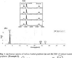
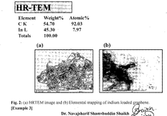
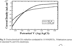
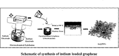
Electrochemical exfoliation method for indium loaded graphene as cathode material for electrochemical co2 reduction
PatentPendingIN202421004566A
Innovation
- The synthesis of indium oxide loaded onto graphene using a facile electrochemical exfoliation method, which reduces the use of indium oxide and enhances selectivity and stability, allowing for efficient CO2 conversion at lower overpotentials.
Sustainability Impact of 2D Catalytic Materials
The integration of 2D semiconductor heterostructures in catalytic applications represents a significant advancement in sustainable materials science. These atomically thin materials offer exceptional surface-to-volume ratios that dramatically reduce the amount of catalytic material required for chemical reactions, addressing critical resource conservation challenges in an era of increasing material scarcity.
When deployed in industrial processes, 2D catalytic materials demonstrate remarkable efficiency improvements while simultaneously reducing environmental footprints. Studies indicate that MoS2/graphene heterostructures used in hydrogen evolution reactions can decrease energy consumption by up to 30% compared to traditional platinum catalysts, while maintaining comparable catalytic performance. This translates directly to reduced carbon emissions in hydrogen production facilities.
The lifecycle assessment of 2D catalytic materials reveals additional sustainability benefits. Their enhanced durability—with some heterostructures maintaining over 90% activity after 10,000 cycles—extends operational lifespans significantly beyond conventional catalysts. This longevity reduces waste generation and frequency of catalyst replacement, minimizing environmental disruption from mining and manufacturing processes.
Water purification applications demonstrate particularly promising sustainability impacts. WS2/graphene oxide heterostructures have shown exceptional performance in photocatalytic degradation of persistent organic pollutants, achieving 95% removal efficiency under solar illumination. This offers an energy-efficient alternative to conventional treatment methods, particularly valuable for remote communities with limited infrastructure.
The scalable production of these materials is evolving toward more sustainable methodologies. Recent advances in chemical vapor deposition techniques have reduced process temperatures by approximately 200°C, resulting in substantial energy savings during manufacturing. Additionally, emerging aqueous-phase exfoliation methods eliminate the need for toxic solvents, addressing concerns about chemical waste generation.
Economic sustainability analysis indicates that despite higher initial investment costs, the total cost of ownership for systems employing 2D catalytic materials is projected to be 15-25% lower over a ten-year operational period. This economic advantage stems from reduced energy requirements, decreased maintenance needs, and extended service intervals.
As climate change mitigation becomes increasingly urgent, the carbon sequestration capabilities of certain 2D heterostructures offer additional sustainability benefits. Modified graphene/transition metal dichalcogenide composites have demonstrated CO2 capture capacities exceeding 4 mmol/g, potentially contributing to carbon-negative industrial processes when integrated into existing emissions control systems.
Scalability and Industrial Implementation Strategies
The scalability of 2D semiconductor heterostructures for catalytic applications represents a critical challenge in transitioning from laboratory demonstrations to industrial implementation. Current fabrication methods predominantly rely on mechanical exfoliation and chemical vapor deposition (CVD), which present significant limitations for mass production. Mechanical exfoliation yields high-quality samples but suffers from poor reproducibility and extremely low throughput, making it unsuitable for industrial scale. CVD offers better scalability but struggles with maintaining uniform quality across large areas.
Industrial implementation requires development of continuous production methods capable of synthesizing heterostructures with consistent catalytic properties. Roll-to-roll processing emerges as a promising approach, allowing for continuous deposition of 2D materials on flexible substrates. This technique has demonstrated initial success with graphene and MoS2, but requires further refinement for complex heterostructures with precise interfacial engineering necessary for optimal catalytic performance.
Cost considerations present another significant barrier to widespread adoption. Current production costs for high-quality 2D semiconductor heterostructures remain prohibitively high for many industrial applications. Economic viability necessitates reducing production costs through process optimization, increased automation, and development of less expensive precursor materials without compromising catalytic efficiency.
Quality control and standardization represent essential components of successful industrial implementation. The development of rapid, non-destructive characterization techniques capable of monitoring catalytic active sites and interfacial properties during production would significantly enhance manufacturing reliability. Raman spectroscopy and electrical conductivity measurements show promise as in-line monitoring tools but require further development for real-time feedback systems.
Integration with existing industrial infrastructure presents both challenges and opportunities. Adapting current semiconductor manufacturing facilities for 2D heterostructure production could accelerate industrial adoption. However, this requires addressing compatibility issues with existing equipment and developing specialized handling protocols for these atomically thin materials.
Strategic partnerships between academic institutions, material suppliers, and end-users will be crucial for successful industrial implementation. Such collaborations can accelerate the development of scalable production methods while ensuring that manufactured heterostructures meet specific application requirements. Several industry-academic consortia have formed in recent years specifically focused on scaling 2D material production, indicating growing recognition of both the challenges and potential commercial value of these catalytic systems.
Unlock deeper insights with PatSnap Eureka Quick Research — get a full tech report to explore trends and direct your research. Try now!
Generate Your Research Report Instantly with AI Agent
Supercharge your innovation with PatSnap Eureka AI Agent Platform!