In-Depth Analysis of 2D Semiconductor Heterostructures in Pharmaceuticals
OCT 21, 20259 MIN READ
Generate Your Research Report Instantly with AI Agent
Patsnap Eureka helps you evaluate technical feasibility & market potential.
2D Semiconductor Heterostructures Background and Objectives
Two-dimensional (2D) semiconductor heterostructures represent a revolutionary class of materials that have emerged from the broader field of 2D materials, which began with the isolation of graphene in 2004. These heterostructures are formed by stacking different 2D materials, such as transition metal dichalcogenides (TMDs), graphene, hexagonal boron nitride (h-BN), and others, to create layered structures with unique electronic, optical, and mechanical properties that differ significantly from their individual components.
The evolution of 2D semiconductor technology has progressed rapidly over the past decade, moving from fundamental research on single-layer materials to the deliberate engineering of multi-layer heterostructures. This progression has been driven by advancements in fabrication techniques, including mechanical exfoliation, chemical vapor deposition (CVD), and molecular beam epitaxy (MBE), which have enabled increasingly precise control over the composition and architecture of these structures.
In the pharmaceutical context, 2D semiconductor heterostructures present unprecedented opportunities for drug delivery, biosensing, and therapeutic applications. Their exceptional surface-to-volume ratio, tunable bandgap, and unique surface chemistry make them particularly promising for targeted drug delivery systems, real-time monitoring of biological processes, and novel therapeutic approaches such as photothermal therapy.
The integration of these materials into pharmaceutical applications represents a convergence of nanotechnology, materials science, and biomedical engineering. Current research trends indicate growing interest in exploiting the quantum confinement effects and surface functionalization capabilities of these materials to develop next-generation pharmaceutical technologies with enhanced efficacy and reduced side effects.
The primary technical objectives of this research include: (1) understanding the fundamental interactions between 2D semiconductor heterostructures and biological systems; (2) developing scalable and reproducible fabrication methods suitable for pharmaceutical applications; (3) engineering biocompatible heterostructures with targeted functionality; and (4) establishing comprehensive safety profiles for these materials in biological environments.
Looking forward, the field is expected to evolve toward more complex heterostructures with multiple functionalities, enabling simultaneous drug delivery, biosensing, and therapeutic effects. The development of "smart" pharmaceutical systems capable of responding to specific biological triggers represents a particularly promising direction, potentially revolutionizing personalized medicine approaches.
This technical research aims to provide a comprehensive assessment of the current state, challenges, and future prospects of 2D semiconductor heterostructures in pharmaceutical applications, with the ultimate goal of accelerating their translation from laboratory research to clinical implementation.
Pharmaceutical Industry Demand Analysis
The pharmaceutical industry is experiencing a significant transformation driven by the integration of advanced materials science, particularly 2D semiconductor heterostructures. Market analysis reveals a growing demand for novel drug delivery systems, diagnostic tools, and therapeutic devices that leverage the unique properties of these nanomaterials. The global pharmaceutical market, valued at over $1.4 trillion, is increasingly investing in nanotechnology-based solutions, with an estimated annual growth rate of 8.5% specifically in nanomedicine applications.
Drug delivery represents the primary demand driver, as pharmaceutical companies seek more precise targeting mechanisms to reduce side effects and improve efficacy. 2D semiconductor heterostructures offer unprecedented control over drug release kinetics through their tunable electronic properties and large surface-to-volume ratios. Market research indicates that targeted drug delivery systems could reduce required drug dosages by up to 70% while maintaining therapeutic efficacy, addressing both cost concerns and patient compliance issues.
Diagnostic applications constitute another significant market segment, with biosensors based on 2D semiconductor heterostructures demonstrating superior sensitivity compared to conventional technologies. The point-of-care diagnostics market is projected to reach $46.7 billion by 2025, with nanomaterial-based sensors capturing an increasing share due to their ability to detect biomarkers at previously unattainable concentrations.
Personalized medicine initiatives are creating additional demand for advanced materials capable of interfacing with biological systems. Pharmaceutical companies are actively seeking technologies that can facilitate real-time monitoring of drug metabolism and therapeutic response. 2D semiconductor heterostructures, with their biocompatibility and electrical properties, are positioned as ideal candidates for implantable monitoring devices and closed-loop drug delivery systems.
Regulatory considerations are shaping market demand patterns, with pharmaceutical companies prioritizing technologies that can accelerate clinical trials and streamline approval processes. The ability of 2D semiconductor heterostructures to enable high-throughput screening and provide detailed pharmacokinetic data aligns with these industry priorities, driving investment in research partnerships between materials science and pharmaceutical sectors.
Cost-effectiveness remains a critical factor influencing adoption rates. While initial implementation costs for 2D semiconductor technologies are high, long-term economic analyses suggest potential savings through improved therapeutic outcomes and reduced hospitalization rates. Market surveys indicate that pharmaceutical executives are increasingly willing to invest in advanced materials that demonstrate clear improvements in clinical outcomes and patient quality of life metrics.
Current Status and Technical Challenges
The global landscape of 2D semiconductor heterostructures in pharmaceutical applications is rapidly evolving, with significant advancements occurring across North America, Europe, and Asia. Currently, research institutions and pharmaceutical companies are exploring these materials primarily for drug delivery systems, biosensing platforms, and therapeutic applications. The United States and China lead in research output, with the EU following closely, particularly in translational research bridging laboratory discoveries with clinical applications.
Despite promising developments, several critical technical challenges persist. The scalable production of high-quality, uniform 2D semiconductor heterostructures remains a significant hurdle. Current fabrication methods such as chemical vapor deposition (CVD) and mechanical exfoliation produce materials with inconsistent properties, limiting pharmaceutical standardization. The batch-to-batch variability presents regulatory challenges for pharmaceutical applications where strict quality control is mandatory.
Biocompatibility and toxicity concerns represent another major obstacle. While preliminary studies suggest acceptable safety profiles for certain 2D materials like MoS2 and WS2, comprehensive long-term toxicity data remains insufficient. The biological interactions between these novel materials and human tissues require extensive investigation before widespread pharmaceutical implementation can occur.
Stability issues in biological environments pose additional challenges. Many 2D semiconductor heterostructures undergo degradation when exposed to physiological conditions, affecting their functional properties and potentially releasing toxic byproducts. Current encapsulation techniques provide only partial solutions, with significant room for improvement in maintaining structural integrity during extended biological exposure.
The integration of 2D semiconductor heterostructures with existing pharmaceutical manufacturing processes presents technical compatibility issues. Traditional pharmaceutical production lines require substantial modification to accommodate these novel materials, creating barriers to industrial adoption. The cost-effectiveness of such integration remains questionable without clear demonstration of superior therapeutic outcomes.
Characterization techniques for these materials in biological contexts are still developing. While advanced microscopy and spectroscopy methods exist for physical characterization, tools specifically designed to evaluate performance in complex biological environments are limited. This creates a knowledge gap between material properties and pharmaceutical functionality.
Regulatory frameworks for pharmaceutical applications of 2D semiconductor heterostructures remain underdeveloped globally. The novel nature of these materials presents classification challenges for regulatory bodies, resulting in uncertain approval pathways. This regulatory uncertainty discourages investment and slows commercial development despite promising research outcomes.
Current Technical Solutions in Pharmaceutical Applications
01 Fabrication methods for 2D semiconductor heterostructures
Various techniques are employed to fabricate 2D semiconductor heterostructures, including molecular beam epitaxy, chemical vapor deposition, and mechanical exfoliation followed by stacking. These methods allow for precise control over layer thickness, composition, and interface quality, which are critical for achieving desired electronic and optical properties in the resulting heterostructures. The fabrication processes often involve careful control of growth conditions such as temperature, pressure, and precursor flow rates to ensure high-quality interfaces between different 2D materials.- Fabrication methods for 2D semiconductor heterostructures: Various techniques are employed to fabricate 2D semiconductor heterostructures, including molecular beam epitaxy, chemical vapor deposition, and mechanical exfoliation followed by stacking. These methods allow for precise control over layer thickness, composition, and interface quality, which are critical for achieving desired electronic and optical properties in the resulting heterostructures. Advanced fabrication approaches enable the creation of atomically thin layers with minimal defects and controlled doping profiles.
- Transition metal dichalcogenide-based heterostructures: Heterostructures based on transition metal dichalcogenides (TMDs) such as MoS2, WS2, MoSe2, and WSe2 exhibit unique electronic and optical properties due to their atomically thin nature. When these materials are stacked together or combined with other 2D materials, they form heterostructures with tunable band alignments and novel quantum phenomena. These structures show promise for applications in electronics, optoelectronics, and quantum information processing due to their strong light-matter interactions and valley-dependent physics.
- Graphene-based 2D heterostructures: Graphene serves as a fundamental building block for many 2D heterostructures due to its exceptional electrical conductivity and mechanical strength. When combined with other 2D materials like hexagonal boron nitride (h-BN) or TMDs, graphene-based heterostructures exhibit enhanced functionality including improved carrier mobility, gate-tunable band gaps, and novel quantum effects. These heterostructures can be designed with specific interlayer coupling to achieve desired electronic properties for next-generation electronic and photonic devices.
- Optoelectronic applications of 2D semiconductor heterostructures: 2D semiconductor heterostructures offer exceptional capabilities for optoelectronic applications due to their direct bandgaps, strong light-matter interactions, and tunable electronic properties. These structures can be engineered to create efficient photodetectors, light-emitting diodes, photovoltaic cells, and optical modulators. The atomically sharp interfaces between different 2D materials enable efficient charge separation and transport, while the ability to tune band alignments allows for optimization of device performance across different wavelength ranges.
- Quantum confinement effects in 2D heterostructures: 2D semiconductor heterostructures exhibit strong quantum confinement effects that significantly alter their electronic and optical properties compared to bulk materials. The confinement of carriers in the atomically thin layers leads to discrete energy levels, enhanced exciton binding energies, and modified band structures. By engineering the layer thickness, composition, and stacking sequence, these quantum effects can be tailored for specific applications in quantum computing, quantum sensing, and quantum communication technologies. The ability to manipulate valley degrees of freedom in these structures also opens possibilities for valleytronics applications.
02 Novel 2D materials for heterostructure applications
Research has focused on developing and characterizing novel 2D materials beyond graphene for use in heterostructures, including transition metal dichalcogenides (TMDs), hexagonal boron nitride (h-BN), and phosphorene. These materials offer diverse electronic properties ranging from semiconducting to insulating behaviors, enabling the design of heterostructures with tailored functionalities. The combination of different 2D materials with complementary properties allows for the creation of devices with enhanced performance characteristics such as improved carrier mobility, tunable bandgaps, and unique optical responses.Expand Specific Solutions03 Electronic and optoelectronic devices based on 2D heterostructures
2D semiconductor heterostructures serve as platforms for next-generation electronic and optoelectronic devices, including field-effect transistors, photodetectors, light-emitting diodes, and solar cells. The atomically thin nature of these materials allows for efficient charge transfer across interfaces and strong light-matter interactions, resulting in devices with high performance and unique functionalities. The ability to precisely control band alignments and quantum confinement effects in these heterostructures enables the development of devices with tailored electronic and optical properties for specific applications.Expand Specific Solutions04 Quantum phenomena in 2D semiconductor heterostructures
2D semiconductor heterostructures exhibit various quantum phenomena due to their reduced dimensionality, including quantum confinement, valley polarization, and exciton formation with high binding energies. These quantum effects can be exploited for applications in quantum information processing, spintronics, and valleytronics. The ability to manipulate these quantum states through external stimuli such as electric fields, magnetic fields, or optical excitation provides opportunities for developing novel quantum devices with enhanced functionality and performance.Expand Specific Solutions05 Integration and scaling of 2D heterostructure technology
Challenges and solutions related to the integration of 2D semiconductor heterostructures with conventional semiconductor technology and scaling for commercial applications are being addressed through innovative approaches. These include developing transfer techniques for large-area heterostructures, improving interface quality between 2D materials and 3D substrates, and establishing reliable contact formation methods. Advances in these areas are essential for transitioning 2D heterostructure technology from laboratory demonstrations to practical applications in commercial electronic and optoelectronic devices.Expand Specific Solutions
Key Industry Players and Competitive Landscape
The 2D semiconductor heterostructures market in pharmaceuticals is currently in an early growth phase, characterized by increasing research activities but limited commercial applications. Market size remains relatively modest but is projected to expand significantly as technological barriers are overcome. From a technical maturity perspective, academic institutions (MIT, Hunan University, Zhejiang University) are driving fundamental research, while established companies are approaching commercialization from different angles. Taiwan Semiconductor Manufacturing Co. and Samsung Electronics bring semiconductor manufacturing expertise, while pharmaceutical players like Kyowa Kirin and F. Hoffmann-La Roche are exploring biomedical applications. Specialized firms such as Innoscience, SOITEC, and Brolis Sensor Technology are developing critical enabling technologies, positioning themselves as potential market leaders as this cross-disciplinary field matures.
SOITEC SA
Technical Solution: SOITEC has developed advanced Smart Cut™ technology adapted specifically for 2D semiconductor heterostructure fabrication in pharmaceutical applications. Their approach enables the transfer of ultra-thin crystalline layers with nanometer precision to create complex heterostructures with tailored properties. For pharmaceutical applications, SOITEC has engineered specialized silicon-on-insulator (SOI) substrates that serve as platforms for growing 2D materials like graphene and hexagonal boron nitride (hBN) with exceptional uniformity[2]. These engineered substrates facilitate the development of highly sensitive biosensors capable of detecting pharmaceutical compounds and monitoring drug delivery processes. SOITEC's technology allows for the creation of multi-layered heterostructures with precisely controlled interfaces, critical for applications such as targeted drug delivery systems and implantable pharmaceutical monitoring devices[4]. Their manufacturing process ensures high reproducibility and yield, addressing key challenges in commercializing 2D semiconductor technologies for pharmaceutical applications.
Strengths: Industry-leading expertise in layer transfer technology; high-volume manufacturing capabilities; exceptional uniformity and reproducibility in substrate production. Weaknesses: Higher initial cost compared to conventional substrates; limited flexibility in post-processing modifications; requires specialized handling and processing equipment.
Taiwan Semiconductor Manufacturing Co., Ltd.
Technical Solution: TSMC has developed a comprehensive platform for integrating 2D semiconductor heterostructures into pharmaceutical analysis and drug delivery systems. Their approach leverages advanced semiconductor manufacturing techniques to create highly uniform and scalable 2D material heterostructures. TSMC's technology involves precise epitaxial growth of transition metal dichalcogenides (TMDs) on specialized substrates with controlled defect density and interface quality[3]. For pharmaceutical applications, TSMC has pioneered the integration of these 2D heterostructures with CMOS technology to create intelligent drug delivery systems with on-chip sensing capabilities. Their platform includes specialized microfluidic channels fabricated using their advanced lithography processes, enabling precise control over drug release profiles and real-time monitoring of pharmaceutical compound interactions[6]. TSMC has demonstrated the capability to manufacture these systems at scale with high yield, addressing a critical barrier to commercialization. Their technology enables pharmaceutical researchers to develop more targeted therapies with reduced side effects through precise spatiotemporal control of drug delivery[8].
Strengths: Unparalleled manufacturing scale and precision; established quality control systems; advanced integration capabilities with existing semiconductor technologies. Weaknesses: Limited experience in biological applications; higher cost structure compared to specialized biotech firms; longer development cycles for novel applications.
Core Patents and Technical Literature Review
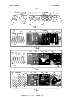
Universal methodology to synthesize diverse two-dimensional heterostructures
PatentWO2017100616A1
Innovation
- A methodology involving selective 'sowing' of aromatic molecule seeds during chemical vapor deposition to grow second two-dimensional materials in voids defined by patterned first materials, enabling both vertical and in-plane 'parallel-stitched' heterostructures between 2D materials, such as graphene-MoS2, WS2-MoS2, and hBN-MoS2, with minimal overlap and precise control.
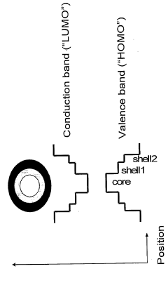
Iii-v semiconductor core-heteroshell nanocrystals
PatentWO2006134599A1
Innovation
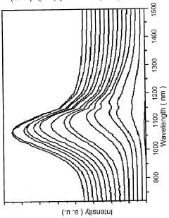
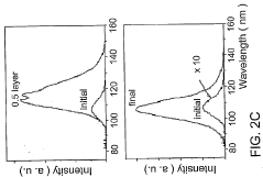
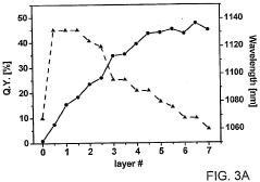
- A core/multishell heterostructure is developed using a layer-by-layer in-solution growth technique, with a III-V semiconductor core coated by multiple shells of different semiconductor materials, each with increasing band gaps, to achieve high photoluminescence quantum yield, stability, and tunable emission across a wide spectral range.
Regulatory Framework for Pharmaceutical Nanotechnology
The regulatory landscape for pharmaceutical nanotechnology, including 2D semiconductor heterostructures, is complex and evolving rapidly across global jurisdictions. The FDA has established specific guidelines for nanomaterials in drug delivery systems, requiring comprehensive characterization of physical properties, stability profiles, and biocompatibility assessments. These regulations emphasize the unique challenges posed by nanoscale materials, including their altered pharmacokinetics and potential for unexpected biological interactions.
In the European Union, the European Medicines Agency (EMA) has implemented the Advanced Therapy Medicinal Products Regulation, which includes provisions for nanomedicine applications. This framework mandates rigorous safety evaluations and quality control measures for pharmaceutical products incorporating 2D semiconductor heterostructures, with particular attention to manufacturing consistency and batch-to-batch reproducibility.
International Harmonization efforts, led by the International Council for Harmonisation of Technical Requirements for Pharmaceuticals for Human Use (ICH), are working to standardize regulatory approaches across regions. However, significant disparities remain in how different countries classify and regulate nanopharmaceuticals, creating challenges for global development and commercialization strategies.
Risk assessment protocols for 2D semiconductor heterostructures in pharmaceutical applications require specialized considerations beyond conventional drug evaluation frameworks. Regulatory bodies increasingly demand long-term stability studies, detailed characterization of surface properties, and comprehensive evaluation of potential degradation products. The unique electronic properties of these materials necessitate additional testing for potential electromagnetic interactions with biological systems.
Good Manufacturing Practice (GMP) requirements for nanopharmaceuticals emphasize controlled production environments, validated analytical methods for characterization, and robust quality management systems. Manufacturers must demonstrate consistent production of heterostructures with precise dimensional control and uniform composition across production batches.
Emerging regulatory trends indicate movement toward adaptive licensing pathways for innovative nanotechnologies, balanced with enhanced post-market surveillance requirements. Several regulatory agencies are developing specialized guidance documents specifically addressing 2D materials in pharmaceutical applications, recognizing their unique properties and potential risks.
Compliance strategies for pharmaceutical developers working with 2D semiconductor heterostructures should include early engagement with regulatory authorities, comprehensive characterization data packages, and robust risk management plans that address the entire product lifecycle from development through post-market monitoring.
Biocompatibility and Safety Considerations
The integration of 2D semiconductor heterostructures into pharmaceutical applications necessitates rigorous assessment of biocompatibility and safety profiles. These novel materials, while promising for drug delivery systems and diagnostic platforms, introduce unique biological interactions that must be thoroughly evaluated before clinical implementation.
Primary biocompatibility concerns center on cellular toxicity mechanisms. Studies indicate that certain 2D materials like graphene oxide can induce oxidative stress in mammalian cells, while transition metal dichalcogenides (TMDs) demonstrate varying cytotoxicity profiles depending on their composition and surface functionalization. MoS2-based heterostructures generally exhibit lower toxicity compared to graphene derivatives, particularly when functionalized with biocompatible polymers such as polyethylene glycol.
Immunological responses represent another critical safety consideration. Recent investigations reveal that the lateral dimensions and surface chemistry of 2D heterostructures significantly influence macrophage activation and pro-inflammatory cytokine production. Materials with dimensions below 100 nm typically demonstrate reduced immune system recognition, while larger structures may trigger more pronounced inflammatory cascades.
Biodegradation pathways and clearance mechanisms must be established for pharmaceutical applications. Unlike conventional drug delivery systems, 2D semiconductor heterostructures present complex degradation profiles influenced by their layered structures and diverse chemical compositions. hBN-based heterostructures have demonstrated favorable degradation in physiological environments, while WS2 structures may persist longer with potential accumulation concerns in specific organs.
Regulatory frameworks for these novel materials remain under development. Current pharmaceutical safety assessment protocols require adaptation to address the unique properties of 2D heterostructures. The FDA has initiated specialized working groups focused on nanomaterial-based pharmaceuticals, with particular attention to 2D materials' distinctive surface-to-volume ratios and quantum confinement effects that may alter biological interactions.
Long-term safety monitoring strategies must be established, as the chronic exposure effects of these materials remain incompletely characterized. Preliminary animal studies suggest minimal systemic toxicity for properly functionalized heterostructures, but comprehensive longitudinal investigations are needed to identify potential delayed adverse effects, particularly regarding neurological and reproductive systems.
Advanced characterization techniques, including super-resolution microscopy and synchrotron radiation analysis, are being deployed to map the biological fate of these materials with unprecedented precision. These methods reveal that surface defects in 2D heterostructures can serve as reactive sites for biomolecular interactions, potentially altering their safety profiles in vivo.
Unlock deeper insights with Patsnap Eureka Quick Research — get a full tech report to explore trends and direct your research. Try now!
Generate Your Research Report Instantly with AI Agent
Supercharge your innovation with Patsnap Eureka AI Agent Platform!