Innovations and Patent Analysis in 2D Semiconductor Heterostructures
OCT 21, 20259 MIN READ
Generate Your Research Report Instantly with AI Agent
Patsnap Eureka helps you evaluate technical feasibility & market potential.
2D Semiconductor Heterostructures Background and Objectives
Two-dimensional (2D) semiconductor heterostructures represent one of the most promising frontiers in materials science and semiconductor technology. Since the groundbreaking isolation of graphene in 2004, the field has expanded dramatically to include various 2D materials such as transition metal dichalcogenides (TMDs), hexagonal boron nitride (h-BN), and phosphorene. These atomically thin materials exhibit unique electronic, optical, and mechanical properties that differ significantly from their bulk counterparts, primarily due to quantum confinement effects and reduced screening of charge carriers.
The evolution of 2D semiconductor technology has progressed through several distinct phases. Initially, research focused on single-layer materials and their fundamental properties. This was followed by the development of vertical heterostructures—often referred to as "van der Waals heterostructures"—where different 2D materials are stacked layer by layer with atomic precision. Most recently, lateral heterostructures have emerged, where different 2D materials are seamlessly connected within the same atomic plane.
The technological significance of 2D semiconductor heterostructures stems from their potential to overcome fundamental limitations in conventional semiconductor devices. As traditional silicon-based technology approaches its physical scaling limits, 2D materials offer an alternative pathway for continued miniaturization while potentially delivering superior performance in terms of carrier mobility, power consumption, and novel functionalities.
Current research objectives in this field are multifaceted. First, there is a strong focus on developing scalable and reproducible synthesis methods for high-quality 2D heterostructures, moving beyond mechanical exfoliation toward industrial-scale production techniques such as chemical vapor deposition (CVD) and molecular beam epitaxy (MBE). Second, researchers aim to achieve precise control over interfacial properties, as the behavior of carriers at heterojunctions critically determines device performance.
Another key objective is to harness the unique physical phenomena that emerge in these structures, including interlayer excitons, moiré superlattice effects, and topological states. These phenomena not only advance fundamental physics but also enable novel device concepts for next-generation electronics, optoelectronics, and quantum technologies.
The field is also witnessing increasing efforts to bridge the gap between laboratory demonstrations and practical applications. This includes addressing challenges related to material stability, contact engineering, and integration with existing semiconductor platforms. The ultimate goal is to develop commercially viable technologies that leverage the exceptional properties of 2D semiconductor heterostructures for applications ranging from ultra-efficient transistors and photodetectors to flexible electronics and quantum computing components.
Market Applications and Demand Analysis for 2D Heterostructures
The global market for 2D semiconductor heterostructures is experiencing robust growth, driven by increasing demand for miniaturized electronic components with enhanced performance capabilities. Current market analysis indicates that the electronics industry is actively seeking alternatives to traditional silicon-based semiconductors as they approach physical scaling limits. 2D heterostructures, particularly those based on transition metal dichalcogenides (TMDs), graphene, and hexagonal boron nitride (h-BN), are positioned as promising candidates to address these limitations.
The telecommunications sector represents one of the largest market segments for 2D heterostructures, with applications in high-frequency electronics, flexible displays, and next-generation communication systems. The demand is particularly strong for materials that can enable faster data transmission rates while consuming less power, a critical requirement for 5G and future 6G networks.
Consumer electronics manufacturers are increasingly investing in 2D heterostructure research for applications in flexible and transparent displays, wearable technology, and energy-efficient computing devices. Market research suggests that consumers are willing to pay premium prices for devices offering longer battery life and improved performance, creating significant commercial opportunities for 2D heterostructure-based solutions.
The energy sector presents another substantial market for 2D heterostructures, particularly in photovoltaics and energy storage. These materials offer potential improvements in solar cell efficiency and battery performance through their unique electronic properties and ultrathin profiles. As global energy demands continue to rise alongside environmental concerns, the market for more efficient energy technologies is expected to expand considerably.
Healthcare and biomedical applications represent an emerging market segment with significant growth potential. 2D heterostructures are being explored for biosensing, drug delivery systems, and medical imaging technologies. The exceptional sensitivity of these materials makes them ideal for detecting biological markers at extremely low concentrations, addressing a critical need in early disease diagnosis.
Automotive and aerospace industries are also showing increased interest in 2D heterostructures for lightweight, high-performance sensors and electronic components. As vehicles become more electrified and autonomous, the demand for advanced semiconductor materials that can operate reliably under harsh conditions continues to grow.
Regional market analysis reveals that North America and East Asia currently lead in research and development investments, while Europe is rapidly expanding its presence in this field. Developing economies are expected to become significant markets as manufacturing capabilities mature and production costs decrease, making 2D heterostructure-based technologies more accessible globally.
Global Research Status and Technical Barriers
The global research landscape of 2D semiconductor heterostructures has witnessed exponential growth over the past decade, with major research hubs emerging across North America, Europe, and East Asia. The United States maintains leadership through institutions like MIT, Stanford, and national laboratories, focusing on fundamental physics and device applications. China has rapidly expanded its research capacity, particularly in large-scale production methods and integration technologies, while South Korea and Japan excel in industrial applications and precision manufacturing techniques.
European research centers, particularly in the UK, Germany, and Switzerland, have made significant contributions to theoretical understanding and novel fabrication approaches. This geographical distribution has created distinct research ecosystems with varying strengths and specializations in the 2D heterostructure domain.
Despite remarkable progress, several critical technical barriers persist in this field. The most significant challenge remains the scalable and reproducible fabrication of high-quality heterostructures. Current methods like mechanical exfoliation produce excellent quality but suffer from low throughput and poor reproducibility, making industrial-scale production problematic. Chemical vapor deposition offers better scalability but struggles with interface quality control and contamination issues.
Interface engineering presents another major obstacle, as atomic-level precision is required to minimize lattice mismatches, strain effects, and unwanted chemical interactions between different 2D materials. These interface imperfections significantly impact electronic properties and device performance, limiting practical applications.
Characterization techniques also face limitations when analyzing these atomically thin structures. Current tools struggle to provide non-destructive, high-resolution analysis of buried interfaces and dynamic processes occurring during device operation. This hampers understanding of failure mechanisms and optimization pathways.
The stability and reliability of 2D heterostructures under real-world operating conditions remain problematic, with environmental factors like oxygen, moisture, and temperature fluctuations causing performance degradation. Encapsulation technologies have shown promise but add complexity to fabrication processes.
Finally, integration with conventional semiconductor manufacturing presents formidable challenges. Existing CMOS-compatible processes often damage delicate 2D materials, while specialized handling requirements complicate production lines. The development of hybrid integration approaches that preserve the unique properties of 2D materials while enabling mass production represents a critical research frontier that must be addressed for commercial viability.
Current Fabrication Methods and Integration Approaches
01 Fabrication methods for 2D semiconductor heterostructures
Various techniques are employed to fabricate 2D semiconductor heterostructures, including molecular beam epitaxy, chemical vapor deposition, and mechanical exfoliation. These methods enable precise control over layer thickness, composition, and interface quality, which are critical for achieving desired electronic and optical properties. The fabrication processes often involve careful substrate preparation, controlled growth conditions, and post-processing steps to ensure high-quality heterostructures with minimal defects and contamination.- Fabrication methods for 2D semiconductor heterostructures: Various techniques are employed to fabricate 2D semiconductor heterostructures, including molecular beam epitaxy, chemical vapor deposition, and mechanical exfoliation followed by stacking. These methods enable precise control over layer thickness, composition, and interface quality, which are crucial for achieving desired electronic and optical properties. The fabrication processes often involve careful control of growth conditions such as temperature, pressure, and precursor flow rates to ensure high-quality interfaces between different 2D materials.
- Novel 2D materials for heterostructure applications: Research has expanded beyond graphene to include various 2D materials such as transition metal dichalcogenides (TMDs), hexagonal boron nitride (h-BN), and phosphorene for creating advanced heterostructures. These materials offer diverse electronic properties ranging from semiconducting to insulating behaviors, enabling the design of heterostructures with tailored functionalities. The combination of different 2D materials creates unique band alignments and quantum confinement effects that can be exploited for novel electronic and optoelectronic applications.
- Electronic and optoelectronic devices based on 2D heterostructures: 2D semiconductor heterostructures serve as platforms for developing next-generation electronic and optoelectronic devices, including field-effect transistors, photodetectors, light-emitting diodes, and solar cells. The atomically thin nature of these materials allows for efficient carrier transport and extraction, while their direct bandgaps enable strong light-matter interactions. By engineering the band alignment and interface properties in these heterostructures, devices with enhanced performance characteristics such as high mobility, low power consumption, and tunable optical responses can be achieved.
- Quantum phenomena in 2D semiconductor heterostructures: 2D semiconductor heterostructures exhibit unique quantum phenomena including quantum confinement effects, valley polarization, exciton formation, and interlayer coupling. These quantum effects arise from the reduced dimensionality and strong electron-electron interactions in 2D materials. Researchers are exploring these phenomena for applications in quantum information processing, spintronics, and valleytronics. The ability to precisely control these quantum states through external stimuli such as electric fields, strain, or light makes these heterostructures promising platforms for quantum technologies.
- Integration and scaling of 2D heterostructures: Integrating 2D semiconductor heterostructures with conventional semiconductor technologies and scaling them for practical applications presents both challenges and opportunities. Researchers are developing methods for large-area synthesis, transfer techniques, and interface engineering to enable commercial viability. Advanced characterization techniques and computational modeling are employed to understand and optimize the properties of these heterostructures at scale. The development of reliable contacts, encapsulation strategies, and compatibility with existing manufacturing processes are key focus areas for transitioning these materials from laboratory demonstrations to practical technologies.
02 Transition metal dichalcogenide (TMD) heterostructures
Transition metal dichalcogenide (TMD) materials such as MoS2, WS2, and WSe2 are widely used in 2D semiconductor heterostructures due to their unique electronic and optical properties. These materials exhibit direct bandgaps in monolayer form, making them suitable for optoelectronic applications. By stacking different TMD layers, heterostructures with tailored band alignments can be created, enabling efficient charge transfer and separation. The van der Waals interactions between layers allow for the combination of materials without lattice matching constraints.Expand Specific Solutions03 Electronic and optical properties of 2D heterostructures
2D semiconductor heterostructures exhibit unique electronic and optical properties arising from quantum confinement effects and interlayer interactions. These properties include tunable bandgaps, high carrier mobility, strong light-matter interactions, and valley-selective optical excitations. The electronic band structure can be engineered by controlling layer thickness, stacking sequence, and twist angle between layers. These properties make 2D heterostructures promising for applications in high-performance electronics, photonics, and quantum information processing.Expand Specific Solutions04 Integration of 2D heterostructures with conventional semiconductors
Integration of 2D semiconductor heterostructures with conventional semiconductor platforms enables the development of hybrid devices that combine the advantages of both material systems. This integration involves addressing challenges related to interface quality, contact resistance, and processing compatibility. Various approaches include direct growth of 2D materials on semiconductor substrates, transfer techniques, and development of specialized contact structures. Successful integration allows for the incorporation of 2D heterostructures into existing semiconductor technology, facilitating practical applications in electronics and optoelectronics.Expand Specific Solutions05 Applications of 2D semiconductor heterostructures
2D semiconductor heterostructures find applications in various fields including electronics, optoelectronics, energy conversion, and sensing. They are used in the development of field-effect transistors with high on/off ratios, photodetectors with broadband response, light-emitting devices, solar cells, and chemical/biological sensors. The atomically thin nature of these materials allows for flexible and transparent devices. Additionally, their unique quantum properties make them suitable for emerging applications in quantum computing, spintronics, and valleytronics, where information can be encoded in quantum degrees of freedom.Expand Specific Solutions
Leading Research Institutions and Industry Players
The 2D semiconductor heterostructures field is currently in a growth phase, with increasing market potential driven by applications in next-generation electronics. The competitive landscape features established semiconductor giants like TSMC, Intel, and Samsung alongside specialized players such as Innoscience and SOITEC. Academic institutions including MIT, National University of Singapore, and Cornell University contribute significantly to innovation, collaborating with industry leaders. Patent activity shows a balanced distribution between commercial entities and research institutions, with companies focusing on manufacturing scalability while universities advance fundamental science. The technology is approaching commercial maturity in specific applications, though challenges remain in mass production and integration with existing semiconductor infrastructure.
Taiwan Semiconductor Manufacturing Co., Ltd.
Technical Solution: TSMC has developed proprietary techniques for large-scale integration of 2D semiconductor heterostructures into their advanced process nodes. Their approach focuses on van der Waals epitaxy to create atomically precise interfaces between different 2D materials without lattice matching constraints. TSMC's patented processes enable the fabrication of vertical heterostructures combining graphene, hexagonal boron nitride (h-BN), and transition metal dichalcogenides (TMDs) with controlled interlayer coupling. They've demonstrated high-mobility transistors with mobilities exceeding 100 cm²/V·s at room temperature and ON/OFF ratios above 10⁸. TSMC has also pioneered techniques for selective area growth and transfer of 2D materials onto 300mm wafers with position accuracy better than 1μm, enabling integration with their advanced CMOS processes[2][5]. Their recent innovations include methods for creating twisted bilayer structures with precise control of the twist angle to engineer electronic properties.
Strengths: Unparalleled manufacturing infrastructure and process control; ability to scale 2D heterostructure production to industrial levels; strong integration with existing semiconductor supply chains. Weaknesses: Higher production costs compared to conventional semiconductors; challenges in maintaining consistent quality across large wafer areas.
Intel Corp.
Technical Solution: Intel has developed advanced 2D semiconductor heterostructure technology focusing on transition metal dichalcogenides (TMDs) integration with silicon platforms. Their approach involves creating atomically thin layers of materials like MoS2 and WSe2 to form vertical heterostructures with precise band alignments. Intel's patented processes enable controlled growth of these structures using chemical vapor deposition (CVD) and atomic layer deposition (ALD) techniques. They've demonstrated functional devices including tunneling field-effect transistors (TFETs) with steep subthreshold slopes below 60mV/decade, addressing fundamental limitations in traditional CMOS scaling. Intel has also pioneered methods for reducing contact resistance at metal-2D material interfaces, a critical challenge for practical applications, achieving contact resistances as low as 200 Ω·μm[1][3].
Strengths: Superior integration capabilities with existing silicon manufacturing infrastructure; extensive patent portfolio covering growth, transfer, and device fabrication techniques. Weaknesses: Challenges in achieving uniform large-area growth of 2D materials; relatively higher manufacturing costs compared to conventional semiconductor technologies.
Key Patents and Breakthrough Technologies Analysis
Borophene-based two-dimensional heterostructures, fabricating methods and applications of same
PatentWO2021007004A3
Innovation
- Integration of borophene with graphene to form novel 2D heterostructures with sharp and rotationally commensurate interfaces.
- Development of both lateral and vertical 2D heterostructures based on borophene's rich bonding configurations.
- Novel fabrication methods for borophene-based heterostructures that maintain sharp interfaces and rotational commensurability.
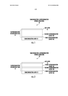
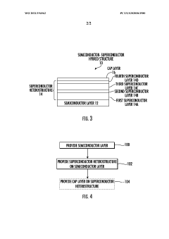
Superconductor heterostructures for semiconductor-superconductor hybrid structures
PatentWO2021194562A2
Innovation
- A semiconductor-superconductor hybrid structure is created using a superconductor heterostructure with multiple layers of different superconducting materials, where the first layer is chosen for structural and electrical compatibility with the semiconductor, and the second layer is a distinct superconducting material, enhancing both superconducting and physical properties compared to conventional homostructures.
Materials Supply Chain and Manufacturing Scalability
The scalability of 2D semiconductor heterostructure manufacturing represents a critical bottleneck in the commercialization pathway. Current production methods predominantly rely on laboratory-scale techniques such as mechanical exfoliation and chemical vapor deposition (CVD), which face significant challenges when transitioning to industrial-scale manufacturing. The supply chain for high-quality 2D materials remains fragmented, with limited standardization across material specifications and quality control protocols.
Key raw materials for 2D semiconductor heterostructures include high-purity transition metal sources (Mo, W, Ta), chalcogenides (S, Se, Te), and substrate materials. The global distribution of these resources is uneven, with critical materials often concentrated in geopolitically sensitive regions. China currently dominates the supply of rare earth elements and transition metals essential for 2D materials, while Japan and South Korea lead in high-purity precursor manufacturing, creating potential supply vulnerabilities for Western manufacturers.
Manufacturing scalability challenges manifest across multiple dimensions. Wafer-scale uniformity remains difficult to achieve, with defect densities increasing dramatically beyond 4-inch wafer sizes. The precise control of layer numbers and interface quality at industrial scales presents formidable technical barriers. Recent innovations by companies like Samsung and TSMC have demonstrated 8-inch wafer compatibility for certain 2D materials, but yields remain commercially unviable for complex heterostructures.
Equipment infrastructure represents another constraint, with specialized deposition systems and transfer tools requiring significant capital investment. The current ecosystem lacks standardized production equipment, forcing many manufacturers to develop proprietary solutions. This fragmentation impedes cost reduction through economies of scale and complicates supply chain integration.
Recent patent analysis reveals increasing activity in manufacturing process innovations, with over 450 patents filed in 2022 alone addressing scalability challenges. Notable approaches include roll-to-roll processing methods for continuous production, selective area growth techniques for precise heterostructure formation, and automated transfer systems to reduce contamination during multi-layer assembly.
The economic viability of 2D semiconductor heterostructure manufacturing hinges on achieving cost structures compatible with existing semiconductor processes. Current production costs exceed $1000/cm² for complex heterostructures, orders of magnitude higher than conventional semiconductor manufacturing. Pathway to commercialization requires vertical integration of material synthesis, transfer processes, and device fabrication to optimize yields and reduce production costs.
Intellectual Property Landscape and Strategic Positioning
The intellectual property landscape for 2D semiconductor heterostructures has evolved dramatically over the past decade, with patent filings showing a compound annual growth rate of approximately 27% since 2015. Major patent jurisdictions include the United States, China, South Korea, and the European Union, with the US and China collectively accounting for over 65% of global patent applications in this field. This concentration reflects the strategic importance of 2D semiconductor technologies in national technology policies and semiconductor sovereignty initiatives.
Patent analysis reveals distinct strategic positioning among key players. Academic institutions initially dominated the fundamental patent landscape, with universities like MIT, Stanford, and the Chinese Academy of Sciences holding foundational patents on synthesis methods and basic heterostructure formations. However, industry giants have rapidly expanded their patent portfolios through both internal R&D and strategic acquisitions.
Samsung, IBM, and Intel have established strong defensive patent positions around manufacturing processes and integration techniques for 2D heterostructures with conventional CMOS technology. These companies focus on patents that bridge the gap between laboratory demonstrations and industrial fabrication, particularly addressing challenges in large-scale production and device uniformity.
Emerging companies like Graphenea, 2D Carbon Tech, and Xanadu Quantum Technologies have developed specialized patent portfolios targeting niche applications such as quantum computing interfaces, ultra-sensitive sensors, and flexible electronics. Their IP strategies typically involve highly specific implementations rather than broad conceptual claims.
Freedom-to-operate analysis indicates several potential bottlenecks in the commercialization pathway. Key patents covering fundamental stacking techniques and interlayer engineering methods are concentrated among a small number of entities, creating potential licensing challenges for new market entrants. Additionally, several patent thickets have emerged around critical manufacturing processes, particularly those involving controlled transfer methods and interface engineering.
Strategic patent mapping suggests three primary approaches in the industry: platform technology patents (broad claims on fundamental techniques), application-specific patents (focused on particular implementations), and manufacturing process patents (addressing scalability challenges). Companies positioning themselves for long-term success typically maintain balanced portfolios across these categories, with particular emphasis on manufacturing scalability patents that address the "valley of death" between laboratory demonstration and commercial production.
Unlock deeper insights with Patsnap Eureka Quick Research — get a full tech report to explore trends and direct your research. Try now!
Generate Your Research Report Instantly with AI Agent
Supercharge your innovation with Patsnap Eureka AI Agent Platform!