Research on 2D Semiconductor Heterostructures and Polymers
OCT 21, 202510 MIN READ
Generate Your Research Report Instantly with AI Agent
Patsnap Eureka helps you evaluate technical feasibility & market potential.
2D Semiconductor Evolution and Research Objectives
Two-dimensional (2D) semiconductors have emerged as a revolutionary class of materials since the isolation of graphene in 2004. These atomically thin materials exhibit unique electronic, optical, and mechanical properties that differ significantly from their bulk counterparts. The evolution of 2D semiconductor research has progressed from initial exploration of graphene to the discovery of transition metal dichalcogenides (TMDs) such as MoS2, WS2, and WSe2, followed by more complex materials including black phosphorus, silicene, and germanene.
The field has witnessed remarkable growth over the past decade, with research publications increasing exponentially from fewer than 100 papers in 2010 to over 5,000 annually by 2022. This surge reflects the scientific community's recognition of the transformative potential these materials hold for next-generation electronics, optoelectronics, and quantum technologies.
Heterostructures, formed by stacking different 2D materials, represent a particularly promising direction. These artificial structures enable precise engineering of electronic band structures and quantum confinement effects, creating opportunities for novel device architectures. The van der Waals forces that hold these layers together allow for unprecedented freedom in combining materials without the constraints of lattice matching that limit conventional semiconductor heterostructures.
Polymer integration with 2D semiconductors has emerged as another frontier, offering pathways to enhance functionality through improved processability, mechanical flexibility, and environmental stability. Polymer-2D semiconductor composites can potentially address key challenges in scalable manufacturing while introducing new functionalities through controlled doping and surface modification.
The primary research objectives in this field include developing scalable synthesis methods for high-quality 2D semiconductors and their heterostructures, understanding and controlling the interfacial physics between different 2D materials and between 2D materials and polymers, and engineering novel electronic and optoelectronic properties through band structure manipulation.
Additionally, researchers aim to explore quantum phenomena in these systems, including exciton physics, valley polarization, and topological states, which could enable quantum information processing applications. The development of practical devices that leverage these unique properties for applications in flexible electronics, photovoltaics, sensors, and energy storage represents another critical objective.
Ultimately, the field seeks to bridge fundamental scientific understanding with technological implementation, addressing challenges in material quality, interface engineering, and device integration to realize the full potential of 2D semiconductor heterostructures and polymer composites in next-generation technologies.
Market Applications of 2D Semiconductor Heterostructures
The market for 2D semiconductor heterostructures is experiencing rapid growth across multiple sectors, driven by their exceptional electronic, optical, and mechanical properties. These atomically thin materials offer unprecedented opportunities for next-generation electronic and optoelectronic devices that traditional semiconductors cannot match.
In the electronics industry, 2D heterostructures are revolutionizing transistor technology. Companies like Samsung and IBM are investing heavily in graphene-based and transition metal dichalcogenide (TMD) heterostructures for ultra-thin, flexible transistors with superior carrier mobility. Market analysis indicates that the semiconductor industry could see a significant shift toward 2D materials for specific applications by 2025, particularly in low-power electronics.
The optoelectronics sector represents another substantial market opportunity. 2D heterostructures demonstrate remarkable light-matter interactions, making them ideal for photodetectors, light-emitting diodes, and photovoltaic cells. The global photodetector market, valued at approximately $38 billion in 2022, is projected to incorporate 2D heterostructure technology increasingly over the next decade, especially in telecommunications and imaging applications.
Flexible electronics constitutes a rapidly expanding market segment where 2D heterostructures hold particular promise. Their mechanical flexibility combined with electronic functionality enables applications in wearable technology, flexible displays, and electronic skin. Market forecasts suggest the flexible electronics sector will grow at a compound annual growth rate of 11% through 2028, with 2D materials playing an increasingly important role.
Energy storage and conversion represent another significant application area. Research on 2D heterostructures for improved battery electrodes, supercapacitors, and catalysts for hydrogen evolution is advancing rapidly. The energy storage market, particularly for electric vehicles and renewable energy systems, presents substantial commercialization opportunities for these materials.
Quantum computing applications are emerging as a high-value niche market. The unique quantum properties of certain 2D heterostructures make them promising candidates for quantum bits and quantum information processing. Though currently in early research stages, this sector could represent a multibillion-dollar opportunity in the coming decades.
Biomedical applications are also gaining traction, with 2D heterostructures being explored for biosensing, drug delivery, and tissue engineering. Their large surface-to-volume ratio and customizable surface chemistry make them particularly suitable for ultrasensitive detection of biomolecules and cellular interactions.
Despite these promising market opportunities, challenges remain in scaling production, ensuring consistency in material quality, and reducing manufacturing costs. The transition from laboratory demonstrations to commercial products requires significant investment in manufacturing technology and quality control processes. Companies that can overcome these challenges stand to capture substantial market share in this emerging technology space.
Technical Barriers in 2D Semiconductor Integration
Despite significant advancements in 2D semiconductor research, several critical technical barriers continue to impede the widespread integration of 2D semiconductor heterostructures and polymers into commercial applications. One of the most persistent challenges is the scalable synthesis of high-quality, large-area 2D materials with consistent properties. Current methods like mechanical exfoliation produce high-quality but small-area flakes unsuitable for industrial applications, while chemical vapor deposition (CVD) struggles with uniformity across large areas and often introduces defects that compromise electronic performance.
Interface engineering presents another significant hurdle, particularly in heterostructures where different 2D materials meet. The van der Waals gaps between layers can lead to contact resistance issues, while lattice mismatches between different materials create strain and potential electronic defects. These interface challenges directly impact carrier mobility and overall device performance, limiting the practical application of theoretical advantages offered by 2D materials.
Contamination control during fabrication remains exceptionally difficult due to the atomically thin nature of these materials. Even minimal exposure to ambient conditions can lead to oxidation, adsorption of water molecules, or introduction of polymer residues during transfer processes, all of which can dramatically alter the electronic properties of 2D semiconductors and their interfaces with polymers.
The integration of 2D materials with traditional CMOS technology presents compatibility issues in terms of processing temperatures, chemical compatibility, and electrical connectivity. Standard semiconductor processing techniques often damage 2D materials, necessitating the development of specialized, low-temperature processes that may not be readily compatible with existing manufacturing infrastructure.
Doping control and contact engineering represent another significant barrier. Unlike bulk semiconductors, conventional doping methods are ineffective for 2D materials due to their ultrathin nature. Alternative approaches such as surface charge transfer doping or electrostatic doping show promise but lack the stability and precision required for commercial applications.
Encapsulation and passivation technologies are still underdeveloped, leaving 2D semiconductor devices vulnerable to environmental degradation. This is particularly problematic for polymer-2D material composites, where the interface stability over time remains questionable under various operating conditions.
Finally, metrology and characterization techniques suitable for atomically thin materials at industrial scales are limited. Current analytical methods often damage samples during measurement or provide insufficient spatial resolution to properly assess defects, interfaces, and electronic properties across large areas, hampering quality control and process optimization efforts.
Current Fabrication Methods for 2D Heterostructures
01 2D Semiconductor Heterostructure Fabrication Methods
Various methods for fabricating 2D semiconductor heterostructures, including layer-by-layer assembly, chemical vapor deposition, and molecular beam epitaxy. These techniques enable the precise control of layer thickness and composition, allowing for the creation of novel electronic and optoelectronic devices with enhanced performance characteristics. The fabrication methods focus on achieving atomically sharp interfaces between different 2D materials to minimize defects and optimize device functionality.- 2D semiconductor heterostructure fabrication methods: Various methods for fabricating 2D semiconductor heterostructures have been developed, including layer-by-layer deposition, chemical vapor deposition, and molecular beam epitaxy. These techniques allow for precise control over the thickness and composition of each layer, enabling the creation of complex heterostructures with tailored electronic and optical properties. The fabrication methods often involve controlling growth parameters such as temperature, pressure, and precursor concentrations to achieve high-quality interfaces between different 2D materials.
- Polymer integration with 2D semiconductor materials: Polymers can be integrated with 2D semiconductor materials to create flexible and stretchable electronic devices. The polymer matrices provide mechanical support and protection for the 2D materials while maintaining their electronic properties. Various techniques such as solution processing, in-situ polymerization, and polymer grafting have been developed to achieve effective integration. These polymer-2D semiconductor composites exhibit enhanced stability, processability, and can be used in applications requiring conformable electronics.
- Optoelectronic applications of 2D semiconductor heterostructures: 2D semiconductor heterostructures exhibit unique optoelectronic properties that make them suitable for various applications including photodetectors, light-emitting diodes, and solar cells. The atomically thin nature of these materials allows for efficient light absorption and emission, while the band alignment in heterostructures enables effective charge separation and transport. By engineering the composition and stacking sequence of different 2D materials, the optical and electronic properties can be tuned to optimize device performance for specific wavelength ranges and applications.
- Interface engineering in 2D heterostructures: Interface engineering plays a crucial role in determining the properties and performance of 2D semiconductor heterostructures. Various approaches have been developed to control and modify the interfaces between different 2D materials, including surface functionalization, insertion of buffer layers, and defect passivation. These techniques help to reduce interfacial resistance, minimize lattice mismatch effects, and enhance charge transfer across the interfaces. Properly engineered interfaces can significantly improve the electrical conductivity, optical response, and overall stability of the heterostructure devices.
- Novel 2D materials and polymer composites for electronic applications: Beyond traditional 2D materials like graphene and transition metal dichalcogenides, novel 2D materials and their polymer composites are being developed for advanced electronic applications. These include 2D metal-organic frameworks, MXenes, and other emerging materials with unique electronic structures. When combined with functional polymers, these materials can form composites with enhanced electrical conductivity, thermal stability, and mechanical flexibility. Such composites are finding applications in energy storage devices, sensors, electromagnetic shielding, and flexible electronics.
02 Polymer Integration with 2D Semiconductors
Integration of polymers with 2D semiconductor materials to create flexible, stretchable electronic devices. Polymers serve as substrates, encapsulation layers, or functional components in these hybrid structures. The polymer integration enhances mechanical properties while maintaining the electronic characteristics of the 2D semiconductors. This approach enables applications in wearable electronics, flexible displays, and biomedical devices where conformability and durability are essential requirements.Expand Specific Solutions03 Optoelectronic Applications of 2D Heterostructures
Development of optoelectronic devices using 2D semiconductor heterostructures, including photodetectors, light-emitting diodes, and photovoltaic cells. The unique band structure and optical properties of 2D materials enable high-performance light-matter interactions. By engineering the heterostructure composition and architecture, researchers can tune the absorption and emission wavelengths, quantum efficiency, and response time of these devices, making them suitable for next-generation optoelectronic applications.Expand Specific Solutions04 Electronic Transport in 2D Heterostructures
Investigation of electronic transport phenomena in 2D semiconductor heterostructures, focusing on carrier mobility, quantum confinement effects, and interfacial properties. The atomically thin nature of these materials leads to unique electronic behaviors including valley polarization, spin-orbit coupling, and topological states. Understanding and controlling these transport mechanisms is crucial for developing high-performance transistors, sensors, and quantum computing components based on 2D materials.Expand Specific Solutions05 Novel 2D Materials and Polymer Composites
Synthesis and characterization of novel 2D semiconductor materials and their composites with functional polymers. These include transition metal dichalcogenides, MXenes, phosphorene, and other emerging 2D materials combined with conductive or insulating polymers. The resulting composites exhibit synergistic properties that can be tailored for specific applications such as energy storage, catalysis, sensing, and electromagnetic shielding. The interface between the 2D materials and polymers plays a critical role in determining the overall performance of these hybrid systems.Expand Specific Solutions
Leading Research Groups and Industry Collaborations
The 2D semiconductor heterostructures and polymers field is currently in a growth phase, with increasing market interest driven by potential applications in next-generation electronics. The global market is expanding rapidly, estimated to reach significant scale as major players invest in R&D. Technologically, the field shows varying maturity levels across different applications. Leading academic institutions (MIT, National University of Singapore, Zhejiang University) are advancing fundamental research, while industry players like TSMC, IBM, and Synopsys are developing commercial applications. Government entities are supporting development through funding initiatives. The ecosystem demonstrates a balanced collaboration between academic research excellence and industrial implementation, with Asian institutions showing particularly strong representation in this emerging field.
National University of Singapore
Technical Solution: NUS has established itself as a leader in 2D semiconductor heterostructure research through their innovative "interface engineering" approach. Their research team has developed proprietary methods for creating atomically clean interfaces between different 2D materials, resulting in enhanced electronic coupling and novel quantum phenomena[1]. NUS researchers have pioneered the use of chemical vapor deposition (CVD) for direct growth of lateral and vertical heterostructures with precisely controlled composition gradients. Their work on "mixed-dimensional" heterostructures, combining 2D semiconductors with 0D quantum dots and 1D nanowires, has opened new avenues for optoelectronic applications[3]. A significant breakthrough from NUS is their development of polymer-based transfer techniques that preserve the intrinsic properties of 2D materials while enabling integration with flexible substrates. They've demonstrated wearable electronics and sensors based on these hybrid structures with exceptional performance metrics[5]. Additionally, NUS has developed novel doping strategies for 2D semiconductors using polymer matrices as carrier reservoirs, allowing precise control over electronic properties[7].
Strengths: World-class expertise in interface engineering; innovative approaches to mixed-dimensional heterostructures; strong focus on practical applications including flexible electronics. Weaknesses: Some techniques require specialized equipment limiting widespread adoption; challenges with long-term stability of polymer-2D material interfaces; limited demonstration of large-area fabrication.
Massachusetts Institute of Technology
Technical Solution: MIT has pioneered research in 2D semiconductor heterostructures through their innovative "layer-by-layer" assembly technique. Their approach involves precise stacking of different 2D materials (including transition metal dichalcogenides, graphene, and hexagonal boron nitride) with atomically clean interfaces to create designer heterostructures with tailored electronic properties[1]. MIT researchers have developed a method to control interlayer twist angles with sub-degree precision, enabling the creation of moiré superlattices that exhibit exotic quantum phenomena such as superconductivity and correlated insulator states[3]. Additionally, they've integrated these 2D heterostructures with polymeric substrates to create flexible, transparent electronics with unprecedented performance characteristics. Their recent breakthrough in creating "programmable" 2D semiconductor heterostructures allows for post-fabrication tuning of electronic properties through applied electric fields or strain engineering[5].
Strengths: Exceptional precision in layer stacking and twist angle control; ability to create designer quantum materials with novel properties; strong integration capabilities with flexible substrates. Weaknesses: Scaling challenges for industrial production; limited thermal stability of some heterostructure configurations; complex fabrication processes requiring specialized equipment.
Breakthrough Patents in 2D Semiconductor-Polymer Interfaces
Borophene-based two-dimensional heterostructures, fabricating methods and applications of same
PatentWO2021007004A3
Innovation
- Integration of borophene with graphene to form 2D heterostructures with sharp and rotationally commensurate interfaces.
- Development of both lateral and vertical 2D heterostructures based on borophene's rich bonding configurations.
- Novel fabrication methods for borophene-based heterostructures that leverage the unique bonding characteristics of boron.
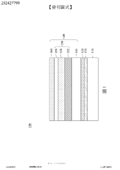
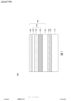
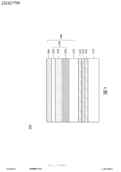
Semiconductor device
PatentActiveTW202427799A
Innovation
- A semiconductor device with a gallium nitride power device on a non-native substrate, utilizing a two-dimensional material layer and intermediate bonding layer to transfer the gallium nitride power element to a thermally conductive substrate, avoiding defects and reducing production costs.

Environmental Impact of 2D Semiconductor Manufacturing
The manufacturing processes for 2D semiconductor heterostructures and polymers present unique environmental challenges that warrant careful consideration. Traditional semiconductor fabrication involves significant resource consumption, hazardous chemicals, and energy-intensive processes. 2D semiconductor manufacturing, while potentially offering some improvements, introduces its own environmental concerns that must be addressed as this technology scales.
Water usage represents a critical environmental factor in 2D semiconductor production. The synthesis and cleaning processes for materials like graphene, transition metal dichalcogenides (TMDs), and hexagonal boron nitride (h-BN) require ultra-pure water in substantial quantities. Current estimates suggest that producing a single 2D semiconductor wafer may consume between 2,000-4,000 gallons of water, creating significant strain on local water resources in manufacturing regions.
Chemical waste management presents another substantial challenge. The exfoliation and transfer processes for 2D materials often employ harsh solvents including N-Methyl-2-pyrrolidone (NMP), dimethylformamide (DMF), and various acids. These chemicals can cause environmental damage if improperly handled or disposed of. Additionally, the etching processes used in creating heterostructures generate waste containing heavy metals and toxic compounds that require specialized treatment facilities.
Energy consumption in 2D semiconductor manufacturing remains high, particularly for processes requiring precise temperature control and ultra-high vacuum conditions. Chemical vapor deposition (CVD) and molecular beam epitaxy (MBE), common techniques for growing high-quality 2D materials, operate at temperatures exceeding 800°C and consume significant electrical power. This energy footprint contributes to greenhouse gas emissions when non-renewable energy sources are utilized.
Raw material sourcing introduces sustainability concerns, particularly regarding rare elements used in certain 2D semiconductors. Materials like indium, gallium, and specific transition metals face supply constraints and often originate from regions with questionable environmental regulations or labor practices. The extraction processes for these materials can lead to habitat destruction, water pollution, and soil contamination.
Emerging polymer-based semiconductor technologies offer potential environmental advantages through reduced processing temperatures and compatibility with solution-based manufacturing. However, these materials introduce new end-of-life challenges related to biodegradability and recycling compatibility that remain largely unresolved in current waste management systems.
Regulatory frameworks for managing the environmental impact of 2D semiconductor manufacturing vary significantly across regions, creating inconsistent standards and enforcement. As production scales from laboratory to industrial levels, comprehensive life cycle assessments and standardized environmental protocols will be essential to minimize ecological damage while maximizing the technological benefits these advanced materials promise.
Scalability Challenges for Commercial Implementation
Despite the promising research advances in 2D semiconductor heterostructures and polymers, significant scalability challenges impede their transition from laboratory innovations to commercial products. Manufacturing processes for 2D materials remain predominantly manual and lab-scale, with techniques like mechanical exfoliation producing high-quality but small-area samples unsuitable for industrial applications. Chemical vapor deposition (CVD) offers better scalability but struggles with maintaining uniform quality across larger substrates.
The precise alignment of different 2D materials to form heterostructures presents another major hurdle. Current methods rely heavily on manual manipulation under microscopes, which is time-consuming and difficult to standardize. Automated assembly systems are emerging but remain in early development stages and lack the precision required for complex heterostructure formation.
Defect control represents a critical challenge for commercial viability. Even minor impurities or structural defects can dramatically alter the electronic properties of 2D materials. Industrial-scale production environments make it exponentially more difficult to maintain the pristine conditions achieved in research laboratories, resulting in performance inconsistencies that undermine product reliability.
Integration with existing semiconductor manufacturing infrastructure presents both technical and economic barriers. The semiconductor industry has invested billions in silicon-based fabrication facilities, and retrofitting these for 2D material production requires substantial capital investment. The temperature and process incompatibilities between traditional semiconductor manufacturing and 2D material synthesis further complicate integration efforts.
Cost factors significantly impact commercial implementation. Current production methods for high-quality 2D materials and heterostructures are prohibitively expensive for mass-market applications. The specialized equipment, low throughput, and high material waste associated with current fabrication techniques result in costs that can only be justified for niche, high-value applications rather than consumer electronics.
Standardization and quality control protocols remain underdeveloped for 2D materials. Unlike silicon, which benefits from decades of established characterization and testing standards, 2D materials lack universally accepted quality metrics. This absence of standardization complicates supplier-manufacturer relationships and creates uncertainty in product specifications, hindering industry adoption.
Environmental stability poses another significant challenge, as many 2D materials and their heterostructures demonstrate sensitivity to oxygen, moisture, and other environmental factors. Developing effective encapsulation technologies that don't compromise device performance while ensuring long-term stability represents a crucial step toward commercial viability.
Unlock deeper insights with Patsnap Eureka Quick Research — get a full tech report to explore trends and direct your research. Try now!
Generate Your Research Report Instantly with AI Agent
Supercharge your innovation with Patsnap Eureka AI Agent Platform!