

Examining Regulatory Frameworks for 2D Semiconductor Heterostructures
OCT 21, 20259 MIN READ
Generate Your Research Report Instantly with AI Agent
PatSnap Eureka helps you evaluate technical feasibility & market potential.
2D Semiconductor Heterostructures Background and Objectives
Two-dimensional (2D) semiconductor heterostructures represent one of the most promising frontiers in materials science and semiconductor technology. Since the groundbreaking isolation of graphene in 2004, the field has expanded dramatically to include various 2D materials such as transition metal dichalcogenides (TMDs), hexagonal boron nitride (h-BN), and phosphorene. These atomically thin materials exhibit unique electronic, optical, and mechanical properties that differ significantly from their bulk counterparts, primarily due to quantum confinement effects and reduced screening of charge carriers.
The evolution of 2D semiconductor technology has progressed through several distinct phases. Initially, research focused on single-layer materials and their fundamental properties. This was followed by the development of vertical heterostructures—often referred to as "van der Waals heterostructures"—where different 2D materials are stacked with atomic precision. Most recently, lateral heterostructures have emerged, where different 2D materials are seamlessly connected in-plane, enabling novel device architectures and functionalities.
Current technological objectives in the field center around overcoming several critical challenges. First is the development of scalable, high-quality synthesis methods that can produce wafer-scale 2D materials with minimal defects and consistent properties. Second is the precise control of interfaces in heterostructures, which significantly influence carrier transport and optoelectronic properties. Third is the integration of 2D heterostructures with conventional semiconductor platforms to leverage existing manufacturing infrastructure.
From a regulatory perspective, the objectives include establishing standardized characterization protocols for 2D materials and heterostructures to ensure consistency across research and industrial applications. Additionally, there is a pressing need to develop safety guidelines for handling and processing these materials, particularly as they move from laboratory settings to commercial production environments.
The long-term technological vision encompasses the realization of ultra-low power electronics, quantum computing components, flexible and transparent electronics, and highly sensitive sensors based on 2D semiconductor heterostructures. These applications could revolutionize computing, telecommunications, healthcare diagnostics, and environmental monitoring.
Understanding the regulatory landscape for these materials is becoming increasingly important as they transition from academic research to commercial applications. Current regulatory frameworks were largely developed for bulk materials and may not adequately address the unique properties and potential risks associated with 2D materials, particularly when considering their high surface-to-volume ratio and potential for novel biological interactions.
Market Analysis for 2D Semiconductor Applications
The 2D semiconductor market is experiencing rapid growth, driven by the unique properties these materials offer compared to traditional semiconductors. The global market for 2D semiconductors was valued at approximately $7.2 billion in 2022 and is projected to reach $21.5 billion by 2030, representing a compound annual growth rate of 14.6%. This growth trajectory is primarily fueled by increasing demand for miniaturized electronic components with enhanced performance characteristics.
Key application segments for 2D semiconductor heterostructures include electronics, optoelectronics, energy storage, and sensing technologies. The electronics sector currently dominates the market share at 42%, followed by optoelectronics at 28%. These applications leverage the exceptional electrical, optical, and mechanical properties of 2D materials such as graphene, transition metal dichalcogenides (TMDs), and hexagonal boron nitride (h-BN).
Regional analysis indicates that North America and Asia-Pacific are the leading markets for 2D semiconductor applications. North America holds approximately 38% of the market share due to substantial research investments and the presence of major technology companies. The Asia-Pacific region follows closely at 35%, with China, South Korea, and Japan emerging as manufacturing powerhouses for 2D semiconductor-based devices.
Consumer electronics represents the largest end-user segment, accounting for 36% of applications. This is followed by telecommunications (24%), automotive (18%), healthcare (12%), and other industries (10%). The integration of 2D semiconductor heterostructures in smartphones, wearable devices, and IoT applications is particularly noteworthy, with adoption rates increasing by 22% annually.
Market challenges include high production costs, scalability issues, and integration complexities with existing semiconductor manufacturing processes. The average cost of producing 2D semiconductor materials remains 3-4 times higher than conventional semiconductors, creating a significant barrier to mass-market adoption.
Emerging opportunities exist in quantum computing, where 2D materials show promise for developing stable qubits, and in flexible electronics, where their mechanical properties enable novel form factors. The quantum computing segment is expected to grow at 29% annually, representing the fastest-growing application area for 2D semiconductor heterostructures.
Customer demand is increasingly focused on sustainability and energy efficiency, with 68% of surveyed electronics manufacturers citing these factors as primary considerations for adopting 2D semiconductor technologies. This trend aligns with global regulatory pushes toward greener technologies and reduced electronic waste.
Global Regulatory Landscape and Technical Barriers
The global regulatory landscape for 2D semiconductor heterostructures remains fragmented, with significant variations across regions. In the United States, the regulatory framework is primarily governed by the Department of Commerce through export control regulations, particularly the Export Administration Regulations (EAR) which classify advanced semiconductor technologies under controlled categories. The recent CHIPS and Science Act has further intensified oversight while simultaneously providing substantial funding for domestic semiconductor research and manufacturing.
The European Union approaches regulation through the European Semiconductor Act, which emphasizes supply chain resilience and technological sovereignty. The EU's regulatory framework places greater emphasis on environmental considerations, requiring manufacturers to adhere to strict sustainability standards in the production and disposal of 2D semiconductor materials, particularly regarding rare earth elements often used in these advanced structures.
In Asia, regulatory approaches diverge significantly. Japan has established the Strategic Innovation Program for semiconductors with streamlined approval processes for research institutions. South Korea's K-Semiconductor Strategy focuses on creating a favorable regulatory environment for domestic manufacturers while maintaining strict intellectual property protections. China's regulatory framework under the 14th Five-Year Plan prioritizes self-sufficiency in semiconductor technology, with fewer restrictions on domestic research but significant barriers for international collaboration.
Technical barriers to global harmonization include the lack of standardized characterization methods for 2D semiconductor heterostructures. The absence of universally accepted testing protocols creates challenges for regulatory compliance across jurisdictions. Material safety data requirements vary substantially between regions, complicating global supply chains and technology transfer.
Export control measures represent another significant barrier, with increasing restrictions on equipment, materials, and knowledge transfer related to advanced semiconductor technologies. These controls have intensified amid geopolitical tensions, creating complex compliance requirements for multinational research collaborations and commercial ventures.
Intellectual property protection frameworks differ substantially across jurisdictions, creating uncertainty in the commercialization of 2D semiconductor technologies. While some regions favor strong patent protections, others emphasize technology transfer and domestic capacity building, creating friction in international research partnerships.
Environmental regulations present additional challenges, with varying requirements for waste management, energy consumption, and chemical usage in the fabrication process. The specialized materials and processes used in 2D semiconductor heterostructures often fall into regulatory gray areas, as existing frameworks were largely designed for traditional semiconductor manufacturing.
Current Compliance Solutions and Frameworks
01 Regulatory compliance for 2D semiconductor heterostructures
Regulatory frameworks governing the development, manufacturing, and commercialization of 2D semiconductor heterostructures require compliance with specific standards and protocols. These regulations ensure the safety, quality, and environmental sustainability of these advanced materials. Companies working with 2D semiconductor heterostructures must navigate various regulatory requirements, including materials classification, risk assessment, and reporting obligations across different jurisdictions.- Regulatory frameworks for 2D semiconductor manufacturing: Regulatory frameworks governing the manufacturing of 2D semiconductor heterostructures focus on standardizing production processes, ensuring quality control, and addressing environmental concerns. These frameworks establish guidelines for the fabrication, handling, and disposal of materials used in 2D semiconductor production. They also outline compliance requirements for manufacturers to ensure that the production of these advanced materials meets safety and environmental standards.
- Safety and environmental regulations for 2D materials: Safety and environmental regulations specific to 2D semiconductor heterostructures address the potential risks associated with nanomaterials. These regulations cover the handling, storage, and disposal of 2D materials to prevent environmental contamination and protect worker health. Guidelines include exposure limits, containment protocols, and waste management procedures for materials such as graphene, transition metal dichalcogenides, and other 2D semiconductors used in heterostructure development.
- Intellectual property frameworks for 2D heterostructure technologies: Intellectual property frameworks govern the protection of innovations in 2D semiconductor heterostructures. These frameworks outline patent application procedures, licensing requirements, and enforcement mechanisms for proprietary technologies. They address challenges specific to 2D materials, such as defining the scope of protection for novel heterostructure compositions, fabrication methods, and applications. The frameworks also establish guidelines for technology transfer and commercialization of 2D semiconductor innovations.
- International standards for 2D semiconductor characterization: International standards for the characterization and testing of 2D semiconductor heterostructures ensure consistency in quality assessment and performance evaluation. These standards define protocols for measuring key properties such as electrical conductivity, optical characteristics, and structural integrity. They establish benchmarks for comparing different heterostructure compositions and fabrication methods, facilitating research collaboration and commercial development across borders.
- Compliance frameworks for 2D semiconductor applications: Compliance frameworks for applications of 2D semiconductor heterostructures outline the regulatory requirements for incorporating these materials into commercial products. These frameworks address sector-specific regulations for electronics, medical devices, energy systems, and other applications. They establish certification processes, performance standards, and safety requirements that must be met before products containing 2D semiconductor heterostructures can enter the market.
02 Environmental and safety standards for 2D semiconductor manufacturing
Manufacturing processes for 2D semiconductor heterostructures are subject to environmental and safety regulations that address potential hazards associated with nanomaterials. These frameworks include guidelines for handling precursor materials, waste management protocols, worker safety measures, and emission controls. Compliance with these standards is essential for sustainable production and minimizing environmental impact while ensuring workplace safety in facilities producing these advanced semiconductor materials.Expand Specific Solutions03 Intellectual property frameworks for 2D semiconductor technologies
Intellectual property protection for innovations in 2D semiconductor heterostructures involves complex regulatory considerations across multiple jurisdictions. Patent frameworks specifically addressing nanomaterials and semiconductor technologies provide guidelines for protecting novel compositions, manufacturing methods, and applications. These regulatory structures influence research collaboration, technology transfer, and commercialization strategies in the rapidly evolving field of 2D semiconductor heterostructures.Expand Specific Solutions04 Import/export controls for 2D semiconductor materials
Regulatory frameworks governing the international trade of 2D semiconductor heterostructures include export controls, import restrictions, and customs regulations. These controls are particularly stringent for materials with potential dual-use applications or strategic importance. Companies must navigate complex compliance requirements when transferring these advanced materials across borders, including proper documentation, licensing, and adherence to international trade agreements specific to semiconductor technologies.Expand Specific Solutions05 Standardization and quality control regulations
Regulatory frameworks for 2D semiconductor heterostructures include standardization requirements that ensure consistency, reliability, and interoperability. These standards address material specifications, testing methodologies, performance metrics, and quality control processes. Compliance with these regulations facilitates industry adoption, enables reliable comparison between different products, and supports integration of these materials into commercial applications. Standardization bodies work with industry stakeholders to develop and update these frameworks as technology advances.Expand Specific Solutions
Key Regulatory Bodies and Industry Stakeholders
The 2D semiconductor heterostructures regulatory landscape is evolving rapidly as the technology transitions from research to commercialization. Currently, the market is in its early growth phase, with significant R&D investments but limited commercial deployment. Major industry players like Taiwan Semiconductor Manufacturing Co., IBM, and Micron Technology are advancing manufacturing capabilities, while research institutions such as MIT, National Taiwan University, and Zhejiang University are driving fundamental innovations. The regulatory framework remains fragmented globally, with different approaches in Asia, North America, and Europe. Technical challenges in standardization, quality control, and intellectual property protection are being addressed through collaborative efforts between industry leaders and academic institutions. As the technology matures, regulatory harmonization will be crucial for market expansion and commercial adoption.
Taiwan Semiconductor Manufacturing Co., Ltd.
Technical Solution: TSMC has established a comprehensive regulatory framework for 2D semiconductor heterostructures that integrates with their advanced semiconductor manufacturing ecosystem. Their approach emphasizes scalable integration of 2D materials into conventional CMOS processes while maintaining strict quality control and regulatory compliance. TSMC's framework includes detailed material qualification protocols that assess the consistency, purity, and performance of 2D materials against established semiconductor industry standards[7]. They've developed specialized contamination control procedures for 2D materials that satisfy both cleanroom requirements and worker safety regulations. TSMC's regulatory approach also addresses intellectual property considerations unique to 2D materials, establishing clear guidelines for patent disclosure and licensing in collaborative development projects. Their framework includes robust reliability testing methodologies that align with JEDEC standards while addressing the unique failure mechanisms of 2D heterostructure devices. TSMC has also worked with international standards organizations to develop specific protocols for evaluating the long-term stability and performance of 2D semiconductor devices in various environmental conditions[8].
Strengths: TSMC's framework benefits from their unparalleled expertise in advanced semiconductor manufacturing and established quality management systems. Their approach effectively addresses the practical challenges of integrating novel materials into high-volume production environments. Weaknesses: The framework is primarily designed for integration with silicon-based technologies and may be less applicable to standalone 2D material systems. Their approach also emphasizes production efficiency which sometimes comes at the cost of flexibility for research applications.
Innoscience (Zhuhai) Technology Co., Ltd.
Technical Solution: Innoscience has developed a specialized regulatory framework for 2D semiconductor heterostructures focused on GaN-based technologies. Their approach addresses the unique challenges of integrating 2D materials with conventional semiconductor manufacturing processes while meeting Chinese and international regulatory requirements. The company has established detailed protocols for material sourcing, quality control, and process validation that comply with both SEMI standards and China's specific semiconductor industry regulations[5]. Their framework includes comprehensive documentation systems that track material provenance and processing parameters, enabling regulatory compliance across global markets. Innoscience has implemented specialized testing methodologies for evaluating the reliability and safety of 2D heterostructure devices, particularly focusing on electrical safety standards and electromagnetic compatibility requirements. Their regulatory approach also addresses end-of-life considerations, including recyclability and hazardous material management in accordance with RoHS and WEEE directives[6].
Strengths: Innoscience's framework is specifically designed for high-volume manufacturing environments and practical implementation in commercial settings. Their approach effectively balances regulatory compliance with production efficiency. Weaknesses: The framework is heavily focused on GaN applications and may require significant adaptation for other 2D material systems. Their approach is also more aligned with Chinese regulatory standards, potentially requiring adjustments for other markets.
Critical Patents and Standards in Regulatory Compliance
2d crystal hetero-structures and manufacturing methods thereof
PatentActiveUS20210005719A1
Innovation
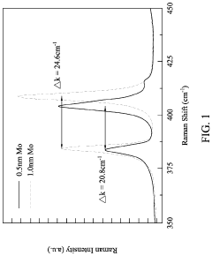
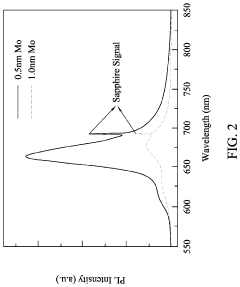
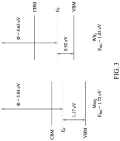
- The development of 2D crystal hetero-structures, specifically WS2/MoS2 hetero-structures, is achieved through chemical vapor deposition or sulfurization, enabling type-II band alignment and increased electron concentration by injecting electrons from WS2 to MoS2, thereby enhancing field-effect mobility and photoluminescence intensity.
Heterostructure having non-volatile actuatable polarization
PatentPendingUS20240162367A1
Innovation
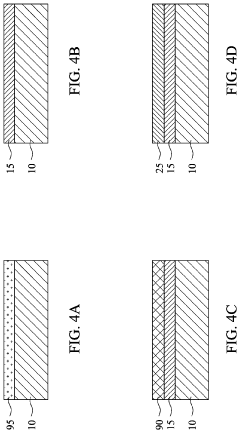
- A heterostructure system comprising a dielectric substrate, a two-dimensional ferroelectric material, and a two-dimensional semiconductor material with a polarization actuation mechanism, where the ferroelectric material is attached to the semiconductor by van der Waals forces, allowing for non-volatile polarization actuation through electrical or optical means, thereby modulating charge concentration and conductivity.
Cross-Border Technology Transfer Considerations
The global nature of semiconductor research and development necessitates careful consideration of cross-border technology transfer regulations when working with 2D semiconductor heterostructures. These novel materials, often developed through international collaboration, face complex regulatory frameworks that vary significantly across jurisdictions. The United States maintains stringent export controls through the Export Administration Regulations (EAR) and International Traffic in Arms Regulations (ITAR), which specifically target advanced semiconductor technologies with potential dual-use applications.
European Union regulations, governed by the EU Dual-Use Regulation (Regulation 2021/821), implement harmonized controls across member states while maintaining certain national discretions. This creates a complex landscape for researchers and companies operating across European borders, particularly when transferring 2D semiconductor technology with potential security implications.
Asian technology powerhouses like Japan, South Korea, and Taiwan have established their own regulatory frameworks that balance innovation promotion with national security concerns. China's export control law, implemented in 2020, has introduced additional complexity to the global semiconductor supply chain, particularly affecting technologies related to 2D materials with strategic importance.
Intellectual property protection presents another critical dimension of cross-border technology transfer. Patent filing strategies must account for different national patent systems, with particular attention to jurisdictions where semiconductor manufacturing occurs. Material transfer agreements (MTAs) have become essential tools when sharing novel 2D heterostructures across borders, specifying usage limitations and ownership of derivative innovations.
Academic collaborations face particular challenges, as universities must navigate between open scientific exchange and compliance with export control regulations. Many institutions have implemented technology control plans specifically addressing 2D materials research with international partners. These plans typically include screening procedures for foreign researchers and segregation of controlled technologies.
Industry partnerships involving 2D semiconductor heterostructures require robust compliance programs that account for the regulatory requirements of all involved countries. Due diligence processes have evolved to include detailed analysis of technology classification, licensing requirements, and end-use verification. Companies increasingly employ specialized legal counsel with expertise in both semiconductor technology and international trade law.
The dynamic nature of both 2D semiconductor technology and global regulations necessitates continuous monitoring of regulatory changes. Organizations must maintain flexible compliance strategies that can adapt to evolving national security priorities and technological advancements in this rapidly developing field.
Environmental and Safety Implications
The emergence of 2D semiconductor heterostructures presents unique environmental and safety considerations that require careful regulatory attention. These atomically thin materials, while promising revolutionary advances in electronics, introduce novel environmental interactions throughout their lifecycle. Manufacturing processes for 2D materials often involve hazardous chemicals, including strong acids and solvents that pose significant environmental risks if improperly managed or released.
Production facilities working with these advanced materials must implement specialized containment systems to prevent nanoparticle release, as the environmental fate and transport mechanisms of 2D materials remain inadequately understood. Current research indicates that some 2D materials, particularly transition metal dichalcogenides containing heavy metals like molybdenum or tungsten, may exhibit toxicity in aquatic ecosystems even at low concentrations.
Workplace safety represents another critical dimension requiring regulatory oversight. Laboratory personnel and manufacturing workers face potential exposure to airborne 2D material particulates, which may present respiratory hazards due to their high surface-area-to-volume ratio and potential for deep lung penetration. Preliminary toxicological studies suggest certain 2D materials may induce oxidative stress and inflammatory responses in biological systems, though long-term health effects remain largely uncharacterized.
End-of-life considerations for 2D semiconductor heterostructure devices present additional challenges. The complex integration of these materials with conventional electronics complicates recycling processes and may lead to improper disposal. The persistence of these materials in the environment and their potential for bioaccumulation require development of specialized waste management protocols and extended producer responsibility frameworks.
Regulatory approaches must balance innovation promotion with precautionary principles. Several jurisdictions have begun adapting existing nanomaterial regulations to address 2D materials specifically, though significant gaps remain. The European Union's REACH regulation provides a potential model through its substance registration requirements, while the U.S. EPA has initiated research programs to evaluate environmental impacts of emerging 2D materials.
International standardization efforts are underway to establish consistent testing methodologies for safety assessment, material characterization, and environmental monitoring. These standards will prove essential for creating harmonized global regulatory frameworks that facilitate responsible development while protecting human health and environmental integrity. Industry stakeholders and academic researchers must collaborate with regulatory bodies to generate the necessary data for evidence-based policy development in this rapidly evolving field.
Unlock deeper insights with PatSnap Eureka Quick Research — get a full tech report to explore trends and direct your research. Try now!
Generate Your Research Report Instantly with AI Agent
Supercharge your innovation with PatSnap Eureka AI Agent Platform!