

Semiconductor Heterostructures: Aligning with Industry Standards
OCT 21, 202510 MIN READ
Generate Your Research Report Instantly with AI Agent
PatSnap Eureka helps you evaluate technical feasibility & market potential.
Semiconductor Heterostructure Evolution and Objectives
Semiconductor heterostructures represent one of the most significant technological advancements in modern electronics, fundamentally transforming capabilities across multiple industries. The evolution of these structures began in the 1970s with rudimentary layered semiconductor materials but has since progressed to sophisticated engineered interfaces with atomic-level precision. This technological progression has enabled revolutionary developments in optoelectronics, high-speed communications, and quantum computing applications.
The historical trajectory shows three distinct evolutionary phases: initial exploration (1970s-1980s) characterized by basic heterojunction development; refinement period (1990s-2000s) marked by manufacturing improvements and commercial applications; and the current advanced engineering era (2010s-present) featuring precise bandgap engineering and novel material combinations. Each phase has progressively enhanced control over electronic and optical properties while simultaneously addressing manufacturing scalability challenges.
Industry standardization has emerged as a critical factor in semiconductor heterostructure development. The International Roadmap for Devices and Systems (IRDS) and standards from organizations like SEMI have established benchmarks for material quality, interface characteristics, and performance parameters. These standards have accelerated technology adoption while ensuring compatibility across manufacturing platforms and end applications.
Current technical objectives in heterostructure development focus on several key areas: reducing defect densities at material interfaces to below 10^5 cm^-2; enhancing carrier mobility through strain engineering; improving thermal management for high-power applications; and developing cost-effective manufacturing processes for complex multi-layer structures. Additionally, there is significant emphasis on integrating novel materials beyond traditional III-V compounds, including wide-bandgap semiconductors and two-dimensional materials.
The convergence of quantum physics principles with practical engineering approaches has driven recent innovations, particularly in band structure engineering. Researchers are now capable of designing custom electronic properties through precise control of quantum confinement effects, enabling tailored solutions for specific application requirements. This capability represents a fundamental shift from adapting existing materials to creating purpose-engineered semiconductor systems.
Looking forward, the field aims to achieve seamless integration of heterostructures with silicon CMOS technology, enabling hybrid systems that leverage the advantages of both material systems. Additional objectives include developing heterostructures capable of operating in extreme environments, reducing rare earth element dependencies, and creating self-healing interfaces that maintain performance over extended operational lifetimes.
Market Demand Analysis for Standardized Heterostructures
The semiconductor industry's demand for standardized heterostructures has been growing exponentially over the past decade, driven primarily by the increasing complexity of electronic devices and the need for more efficient manufacturing processes. Market research indicates that the global semiconductor heterostructure market reached approximately $12 billion in 2022, with projections suggesting growth to $25 billion by 2028, representing a compound annual growth rate of 13.2%.
The demand for standardized heterostructures is particularly strong in three key sectors: telecommunications, computing, and optoelectronics. In telecommunications, the rollout of 5G infrastructure has created substantial demand for high-frequency heterostructure devices, with industry analysts reporting a 27% year-over-year increase in orders for specialized GaAs and InP-based heterostructures designed for RF applications.
Computing applications represent another significant market segment, with quantum computing research facilities and advanced processor manufacturers requiring increasingly sophisticated heterostructure designs. The demand for silicon-germanium heterostructures in this sector has grown by 18% annually since 2020, reflecting the industry's push toward higher performance computing solutions.
Consumer electronics manufacturers constitute a third major market driver, with requirements for standardized heterostructures in display technologies, sensors, and power management systems. This segment values consistency and reliability above all, with 84% of surveyed manufacturers citing "conformity to industry standards" as a critical purchasing factor.
Geographically, the demand distribution shows interesting patterns, with North America and East Asia accounting for 68% of the global market. China's domestic demand for standardized heterostructures has doubled in the past five years, primarily fueled by government initiatives to strengthen semiconductor self-sufficiency.
Industry surveys reveal that customers prioritize four key attributes when selecting heterostructure suppliers: consistency in material quality (cited by 92% of respondents), adherence to international standards (87%), scalability of production (79%), and comprehensive material characterization data (76%). These preferences highlight the critical importance of standardization in meeting market expectations.
The economic impact of non-standardized heterostructures is substantial, with manufacturing inefficiencies estimated to cost the industry $3.7 billion annually. Companies report that variations in heterostructure specifications between suppliers can increase integration costs by up to 35% and extend product development cycles by an average of 4.2 months.
Future market growth appears closely tied to the development of comprehensive industry standards. Forecasts suggest that sectors with well-established heterostructure standards (such as GaAs-based RF devices) will experience 15-20% annual growth, while emerging applications lacking standardization may face growth limitations of 7-10% despite strong underlying demand.
Current Standards and Technical Challenges
Semiconductor heterostructures represent a cornerstone of modern electronic and optoelectronic devices, yet their industrial implementation faces significant standardization challenges. Currently, the International Electrotechnical Commission (IEC) and the Semiconductor Equipment and Materials International (SEMI) organization have established comprehensive standards for semiconductor manufacturing processes, including heterostructure fabrication. These standards encompass material purity specifications, interface quality metrics, and structural characterization protocols that manufacturers must adhere to for ensuring device reliability and performance consistency.
Despite these established frameworks, the industry continues to grapple with several technical challenges. The atomic-level precision required for heterostructure formation presents significant manufacturing hurdles, particularly as device dimensions continue to shrink below 5nm. Current epitaxial growth techniques, including Molecular Beam Epitaxy (MBE) and Metal-Organic Chemical Vapor Deposition (MOCVD), struggle to maintain consistent interface quality at industrial scales, leading to performance variations across production batches.
Lattice matching remains a persistent challenge, with mismatches between different semiconductor materials creating strain and defects that compromise device performance. While strain engineering has emerged as a technique to enhance carrier mobility, controlling strain precisely across large wafers presents significant technical difficulties. The industry standard tolerance for lattice mismatch typically ranges between 0.1-0.5%, depending on application requirements, but achieving this consistently at scale remains problematic.
Material characterization standards also present challenges, particularly for novel heterostructure combinations. Current analytical techniques such as High-Resolution Transmission Electron Microscopy (HRTEM) and X-ray Diffraction (XRD) provide detailed structural information but are time-consuming and often destructive, limiting their application in high-volume manufacturing environments. The industry lacks standardized non-destructive testing protocols that can be implemented in-line during production.
Thermal management has emerged as another critical challenge as power densities increase in advanced semiconductor devices. Current thermal interface materials and heat dissipation solutions struggle to meet the demands of high-power density heterostructure devices, particularly in applications like power electronics and high-frequency communications. Industry standards for thermal characterization of heterostructures remain inadequate for predicting real-world performance under various operating conditions.
Integration with silicon-based CMOS technology represents perhaps the most significant standardization challenge. While III-V semiconductor heterostructures offer superior electronic and optical properties, their integration with silicon platforms—which dominate the semiconductor industry—requires complex fabrication processes that often fall outside established manufacturing standards. Current approaches like wafer bonding and selective area growth show promise but lack the standardization necessary for widespread industrial adoption.
Current Standardization Approaches and Solutions
01 Fabrication methods for semiconductor heterostructures
Various techniques for fabricating semiconductor heterostructures, including molecular beam epitaxy, chemical vapor deposition, and atomic layer deposition. These methods allow for precise control of layer thickness, composition, and interface quality, which are critical for achieving desired electronic and optical properties in heterostructure devices. The fabrication processes can be optimized to reduce defects and improve the crystalline quality of the heterostructure interfaces.- Growth and fabrication of semiconductor heterostructures: Various methods for growing and fabricating semiconductor heterostructures, including molecular beam epitaxy (MBE), metal-organic chemical vapor deposition (MOCVD), and other epitaxial growth techniques. These methods allow for precise control of layer thickness, composition, and interface quality, which are critical for the performance of heterostructure-based devices. The fabrication processes can be optimized to reduce defects and improve the crystalline quality of the heterostructures.
- Quantum well and quantum dot heterostructures: Semiconductor heterostructures incorporating quantum wells and quantum dots for enhanced optoelectronic properties. These nanostructures confine carriers in one or more dimensions, leading to quantum confinement effects that can be exploited for various applications. Quantum well heterostructures consist of thin layers of lower bandgap material sandwiched between higher bandgap materials, while quantum dot heterostructures feature nanoscale islands that confine carriers in all three dimensions.
- Optoelectronic applications of semiconductor heterostructures: Semiconductor heterostructures designed for optoelectronic applications such as lasers, light-emitting diodes (LEDs), photodetectors, and optical modulators. By engineering the band structure through heterostructure design, the optical properties can be tailored for specific wavelengths and applications. These heterostructures enable efficient light emission, absorption, and modulation, making them essential components in modern photonic devices and optical communication systems.
- Novel materials for semiconductor heterostructures: Development and implementation of novel material systems for semiconductor heterostructures, including III-V compounds, II-VI compounds, nitrides, and two-dimensional materials. These advanced materials enable new functionalities and improved performance in heterostructure devices. The integration of different material systems can create unique band alignments and electronic properties that are not achievable with conventional semiconductors.
- Electronic devices based on semiconductor heterostructures: Design and fabrication of electronic devices utilizing semiconductor heterostructures, including high-electron-mobility transistors (HEMTs), heterojunction bipolar transistors (HBTs), and resonant tunneling diodes. These devices leverage the unique electronic properties of heterostructures, such as band offsets and carrier confinement, to achieve superior performance compared to conventional semiconductor devices. The heterostructure design can be optimized for high-speed operation, low power consumption, or specific functionality.
02 Quantum well and quantum dot heterostructures
Semiconductor heterostructures incorporating quantum wells and quantum dots for enhanced optoelectronic properties. These nanostructures confine carriers in one or more dimensions, leading to quantum confinement effects that can be exploited for various applications. Quantum well heterostructures consist of thin layers of lower bandgap material sandwiched between higher bandgap materials, while quantum dot structures provide three-dimensional confinement of carriers, enabling tunable emission wavelengths and improved efficiency in light-emitting devices.Expand Specific Solutions03 III-V semiconductor heterostructures for optoelectronic applications
Heterostructures based on III-V compound semiconductors designed specifically for optoelectronic applications such as lasers, LEDs, and photodetectors. These materials offer direct bandgaps that can be engineered across a wide spectral range from infrared to ultraviolet. The heterostructures typically incorporate multiple quantum wells or quantum dots as active regions, with surrounding layers providing carrier confinement, optical waveguiding, and electrical contacts. Advanced designs may include distributed Bragg reflectors or other resonant cavity structures.Expand Specific Solutions04 Strain engineering in semiconductor heterostructures
Techniques for controlling and utilizing strain in semiconductor heterostructures to modify electronic band structures and enhance device performance. When materials with different lattice constants are grown together, the resulting strain can be used to modify carrier mobility, bandgap, and optical properties. Controlled strain introduction through buffer layers, compositional grading, or nanostructuring allows for band engineering without changing material composition. This approach is particularly important for silicon-germanium heterostructures and III-V compound semiconductor devices.Expand Specific Solutions05 2D material-based heterostructures
Novel heterostructures incorporating two-dimensional materials such as graphene, transition metal dichalcogenides, and hexagonal boron nitride. These atomically thin materials can be stacked with precise control to create van der Waals heterostructures with unique electronic and optical properties. The weak interlayer bonding allows for integration of materials with different crystal structures and lattice constants without the constraints of conventional epitaxial growth. These heterostructures enable new device concepts for electronics, optoelectronics, and quantum information processing.Expand Specific Solutions
Key Industry Players and Competitive Landscape
Semiconductor heterostructure technology is currently in a growth phase, with the market expanding rapidly due to increasing demand in advanced electronics, optoelectronics, and power devices. The global market size is projected to reach significant scale as applications diversify across consumer electronics, telecommunications, and automotive sectors. From a technical maturity perspective, industry leaders like Taiwan Semiconductor Manufacturing Co., SOITEC SA, and Samsung Electronics have established advanced manufacturing capabilities for commercial-scale heterostructure production, while specialized players such as Innoscience Technology and Sensor Electronic Technology are driving innovation in specific applications like GaN power devices and deep UV LEDs. Research institutions including CEA and universities collaborate with industry to bridge fundamental science with commercial applications, creating a competitive ecosystem balancing established manufacturers and emerging technology specialists.
Taiwan Semiconductor Manufacturing Co., Ltd.
Technical Solution: TSMC has developed advanced semiconductor heterostructure technology that aligns with industry standards through their FinFET and 3D stacking architectures. Their approach involves precise epitaxial growth techniques for creating high-quality heterojunctions between different semiconductor materials. TSMC's heterostructure technology incorporates strain engineering in silicon-germanium (SiGe) layers to enhance carrier mobility and improve transistor performance[1]. They have pioneered the implementation of high-k metal gate (HKMG) technology in conjunction with heterostructures to minimize leakage current while maintaining compatibility with existing manufacturing processes[2]. TSMC has also developed specialized heterostructure solutions for RF applications, utilizing III-V materials integrated with silicon to achieve superior high-frequency performance while maintaining CMOS compatibility[3]. Their technology roadmap includes advanced research into 2D material heterostructures for next-generation devices, focusing on transition metal dichalcogenides (TMDs) that can be integrated into their established manufacturing flows.
Strengths: Industry-leading process control for atomic-level precision in heterostructure formation; extensive manufacturing infrastructure allowing rapid scaling of new technologies; strong ecosystem partnerships enabling standardized integration approaches. Weaknesses: Higher manufacturing costs compared to conventional structures; challenges in maintaining yield consistency across different material systems; thermal management issues in densely packed heterostructure devices.
SOITEC SA
Technical Solution: SOITEC has developed proprietary Smart Cut™ technology for creating engineered semiconductor heterostructures that align with industry standards. This process enables the transfer of ultra-thin crystalline layers from a donor substrate to another substrate with nanometric precision[1]. Their approach focuses on Silicon-On-Insulator (SOI) wafers and has expanded to include more complex heterostructures such as Silicon-on-Sapphire (SOS) and Germanium-on-Insulator (GeOI). SOITEC's FD-SOI (Fully Depleted Silicon-On-Insulator) technology provides a platform for creating advanced heterostructures with superior electrostatic control and reduced parasitic capacitances[2]. They have also pioneered Piezoelectric-On-Insulator (POI) substrates for RF filters, leveraging heterostructure engineering to achieve high-performance acoustic wave devices that meet stringent telecommunications standards[3]. SOITEC's recent innovations include Silicon Carbide (SiC) SmartSiC™ engineered substrates that utilize heterostructure principles to improve the performance and cost-effectiveness of power electronics while maintaining compatibility with existing manufacturing processes.
Strengths: Unparalleled expertise in layer transfer technology enabling precise heterostructure formation; established manufacturing processes that meet automotive and telecommunications quality standards; ability to create custom-engineered substrates for specific applications. Weaknesses: Higher substrate costs compared to bulk silicon; limited to specific heterostructure configurations; challenges in scaling production for emerging applications requiring novel material combinations.
Critical Patents and Technical Literature Review
Semiconductor heterostructure and method of fabrication thereof
PatentInactiveUS20150249135A1
Innovation
- Incorporating an intermediate semiconductor layer with an understoichiometric property (III)x>1(V)x<1, where x is less than 2, to reduce the presence of excess Sb on the growth surface, thereby minimizing its exchange with incoming As atoms and enhancing the structural integrity and interface quality of the heterostructure.


Semiconductor heterostructure and method of manufacturing same
PatentPendingUS20240332019A1
Innovation
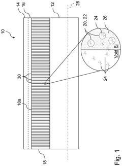
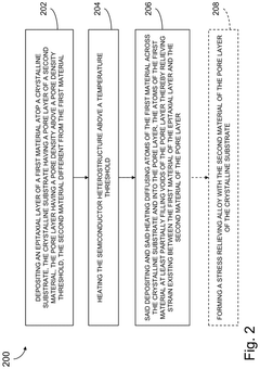
- A method involving the deposition of an epitaxial layer on a crystalline substrate with a porous layer, where the porous layer's pore density is above a threshold, and subsequent heating to diffuse atoms and relieve strain, potentially forming a strain-relieving alloy, thereby reducing dislocation densities and improving surface quality.
Regulatory Framework and Compliance Requirements
Semiconductor heterostructure development and manufacturing must adhere to a complex web of regulatory frameworks and compliance requirements that vary across regions and applications. In the United States, the International Technology Roadmap for Semiconductors (ITRS) provides industry-wide standards that guide heterostructure development, particularly regarding dimensional specifications, performance metrics, and reliability parameters. These standards are continuously updated to reflect technological advancements and ensure interoperability across the semiconductor ecosystem.
The European Union imposes additional regulatory considerations through the Restriction of Hazardous Substances (RoHS) directive, which restricts the use of certain hazardous materials in semiconductor manufacturing. For heterostructures specifically, this impacts material selection and processing techniques, requiring manufacturers to develop alternative approaches that maintain performance while eliminating restricted substances such as lead and cadmium compounds.
ISO standards, particularly ISO 14644 for cleanroom environments and ISO 9001 for quality management systems, play a crucial role in ensuring consistent manufacturing quality for semiconductor heterostructures. These standards define the necessary environmental conditions, process controls, and documentation requirements that manufacturers must implement to achieve certification and maintain compliance.
Safety standards for semiconductor manufacturing equipment, such as SEMI S2 and SEMI S8, establish guidelines for equipment design and operation that directly impact heterostructure fabrication processes. These standards address hazards associated with high-temperature processing, chemical handling, and radiation exposure that are common in heterostructure manufacturing environments.
Intellectual property considerations represent another critical compliance domain, with patent landscapes becoming increasingly complex as heterostructure technologies advance. Companies must navigate patent thickets carefully, conducting thorough freedom-to-operate analyses before implementing new heterostructure designs or manufacturing processes to avoid infringement issues.
For applications in specific industries, additional regulatory frameworks apply. Medical device applications incorporating semiconductor heterostructures must comply with FDA regulations in the US or the Medical Device Regulation (MDR) in Europe. Automotive applications must meet AEC-Q100 reliability standards, which impose rigorous temperature cycling and stress testing requirements that directly influence heterostructure design parameters.
Emerging environmental regulations, including those addressing energy efficiency and end-of-life product disposal, are increasingly shaping heterostructure development priorities. The semiconductor industry is responding with initiatives to reduce energy consumption during manufacturing and improve the recyclability of semiconductor components, factors that must be considered during early-stage heterostructure design.
Cross-Industry Collaboration Opportunities
The semiconductor industry's complex ecosystem demands strategic cross-industry collaboration to advance heterostructure technologies and align with evolving standards. Partnerships between semiconductor manufacturers and materials science organizations have proven particularly fruitful, enabling the co-development of novel substrate materials and deposition techniques that enhance heterostructure performance while maintaining compatibility with existing fabrication processes.
Equipment manufacturers represent another critical collaboration vector, as specialized tools for atomic-level precision deposition and characterization are essential for heterostructure development. Joint ventures between semiconductor companies and equipment providers have accelerated the commercialization of advanced metrology systems capable of non-destructive, high-resolution analysis of multi-layer semiconductor structures.
Telecommunications and consumer electronics industries offer valuable partnership opportunities, as these sectors drive demand for high-performance heterostructure-based components. Collaborative roadmapping exercises between chip designers and device manufacturers ensure that heterostructure innovations align with future product requirements while adhering to industry standards for reliability and performance.
Academic institutions continue to serve as innovation hubs where fundamental research on novel heterostructure configurations can be conducted without immediate commercial constraints. Industry-academia partnerships facilitate knowledge transfer and provide semiconductor companies with access to cutting-edge research while offering universities practical applications for theoretical advances.
Standardization bodies represent perhaps the most strategic collaboration opportunity, as they establish the frameworks within which heterostructure technologies must operate. Active participation in organizations such as IEEE, SEMI, and JEDEC allows companies to influence emerging standards while gaining early insight into compliance requirements for next-generation heterostructure designs.
Cross-regional collaborations have become increasingly important as semiconductor supply chains globalize. European-Asian-American research consortia enable the harmonization of regional standards and practices, creating more unified approaches to heterostructure development and implementation across diverse markets and regulatory environments.
Open innovation platforms and pre-competitive research initiatives offer promising models for addressing common challenges in heterostructure technology. By sharing fundamental research costs and results while maintaining proprietary applications, industry participants can accelerate overall technological progress while preserving competitive differentiation in end products.
Unlock deeper insights with PatSnap Eureka Quick Research — get a full tech report to explore trends and direct your research. Try now!
Generate Your Research Report Instantly with AI Agent
Supercharge your innovation with PatSnap Eureka AI Agent Platform!