

How 2D Semiconductor Heterostructures Transform Electronic Fabrication
OCT 21, 202510 MIN READ
Generate Your Research Report Instantly with AI Agent
PatSnap Eureka helps you evaluate technical feasibility & market potential.
2D Semiconductor Evolution and Objectives
Two-dimensional (2D) semiconductors have emerged as a revolutionary class of materials since the groundbreaking isolation of graphene in 2004. Unlike traditional three-dimensional bulk semiconductors, these atomically thin materials exhibit unique electronic, optical, and mechanical properties that arise from quantum confinement effects and reduced dimensionality. The evolution of 2D semiconductors began with graphene but quickly expanded to include transition metal dichalcogenides (TMDs) such as MoS2, WS2, and WSe2, as well as other materials like hexagonal boron nitride (h-BN) and phosphorene.
The technological trajectory of 2D semiconductors has been marked by significant milestones. Following the initial discovery phase, researchers focused on fundamental property characterization, developing synthesis methods, and exploring basic device applications. The field then progressed toward more sophisticated heterostructure engineering—the deliberate stacking and integration of different 2D materials to create novel functionalities that exceed those of individual components.
Recent advancements have centered on precise control over layer thickness, interfacial properties, and defect engineering. The ability to manipulate these parameters has enabled researchers to tailor electronic band structures, create quantum wells, and design materials with programmable properties. This evolution represents a paradigm shift from traditional semiconductor fabrication approaches, which rely heavily on doping and complex processing techniques.
The primary technical objectives in this field now focus on several key areas. First, developing scalable and reproducible synthesis methods that can transition from laboratory demonstrations to industrial production. Second, achieving precise control over heterostructure interfaces to minimize undesirable effects such as charge trapping and scattering. Third, engineering novel heterostructures with properties specifically designed for applications in electronics, optoelectronics, and quantum information processing.
Another critical objective is overcoming the challenges of integration with existing silicon-based technologies. This includes developing compatible processing techniques, addressing issues of contact resistance, and ensuring long-term stability under operational conditions. Researchers are also exploring how 2D semiconductor heterostructures can enable entirely new device architectures that transcend the limitations of conventional electronics.
The ultimate goal is to leverage the unique properties of 2D semiconductor heterostructures to create a new generation of electronic devices characterized by atomic-scale thickness, mechanical flexibility, enhanced performance, and novel functionalities. These advances aim to address the increasing demands for miniaturization, energy efficiency, and performance in next-generation computing, communications, sensing, and energy conversion technologies.
Market Demand for Advanced Electronic Fabrication
The global market for advanced electronic fabrication technologies is experiencing unprecedented growth, driven by the increasing demand for smaller, faster, and more energy-efficient electronic devices. The emergence of 2D semiconductor heterostructures represents a paradigm shift in this landscape, offering solutions to the limitations of traditional silicon-based technologies. Market research indicates that the semiconductor industry, valued at approximately $600 billion in 2023, is projected to reach $1 trillion by 2030, with advanced fabrication technologies accounting for a significant portion of this growth.
Consumer electronics continues to be the primary driver of demand, with smartphones, tablets, and wearable devices requiring increasingly sophisticated components that can deliver enhanced performance while consuming less power. The global smartphone market alone, with annual shipments exceeding 1.2 billion units, creates substantial demand for next-generation semiconductor technologies that can enable thinner devices with longer battery life.
The automotive sector represents another rapidly expanding market for advanced electronic fabrication. The transition toward electric vehicles and autonomous driving systems has intensified the need for high-performance, reliable semiconductor components. Industry analysts project that semiconductor content in vehicles will double by 2027, creating a market opportunity exceeding $100 billion annually.
Data centers and cloud computing infrastructure constitute a third major demand driver. With global data creation projected to exceed 180 zettabytes by 2025, the need for more efficient computing architectures has never been greater. 2D semiconductor heterostructures offer promising solutions for reducing energy consumption in data centers, which currently account for approximately 1% of global electricity usage.
The telecommunications industry, particularly with the ongoing deployment of 5G networks and development of 6G technologies, represents another significant market opportunity. These advanced networks require components capable of operating at higher frequencies with greater efficiency than conventional silicon-based devices can provide.
Industrial IoT applications are emerging as a substantial market segment, with manufacturing, logistics, and utility companies increasingly deploying sensor networks and edge computing systems that benefit from the unique properties of 2D semiconductor heterostructures. The industrial IoT market is growing at a compound annual rate exceeding 20%, creating sustained demand for advanced fabrication technologies.
Healthcare technology represents a promising growth area, with medical devices, diagnostic equipment, and wearable health monitors requiring increasingly sophisticated electronic components. The medical electronics market is projected to reach $8.8 billion by 2027, with advanced semiconductor technologies playing a crucial role in enabling new capabilities and form factors.
Current State and Challenges in 2D Heterostructures
The global landscape of 2D semiconductor heterostructures has witnessed remarkable progress in recent years, with significant advancements in material synthesis, characterization, and device fabrication. Currently, researchers have successfully demonstrated the creation of various heterostructures using transition metal dichalcogenides (TMDs), graphene, hexagonal boron nitride (h-BN), and other 2D materials. These structures exhibit exceptional electronic, optical, and mechanical properties that conventional bulk semiconductors cannot achieve.
In the United States and Europe, research institutions have made substantial progress in developing precise layer-by-layer assembly techniques, while Asian countries, particularly China, South Korea, and Japan, have demonstrated strengths in large-scale production methods and novel applications. Despite these advancements, significant technical challenges persist across the global research community.
The primary technical hurdle remains the scalable and reproducible fabrication of high-quality heterostructures. Current methods like mechanical exfoliation produce high-quality but small-area flakes unsuitable for industrial applications. Chemical vapor deposition (CVD) offers larger coverage but struggles with interface quality and precise thickness control. The presence of contaminants, lattice mismatches, and defects at interfaces significantly impacts device performance and reliability.
Another critical challenge is the development of reliable electrical contacts to 2D materials. Traditional metal deposition techniques often introduce damage to the delicate 2D layers or create Schottky barriers that limit device performance. Researchers are exploring various approaches including edge contacts, phase-engineered contacts, and intercalation doping to overcome these limitations.
Integration with existing semiconductor manufacturing infrastructure presents additional obstacles. The temperature sensitivity of many 2D materials makes them incompatible with standard CMOS processing conditions. Furthermore, current metrology tools are not optimized for characterizing atomically thin layers, making quality control difficult at industrial scales.
Environmental stability remains a significant concern, as many 2D materials are susceptible to degradation when exposed to ambient conditions. Encapsulation techniques using h-BN or other protective layers show promise but add complexity to the fabrication process.
From a geographical perspective, research centers in the United States (MIT, Stanford, Berkeley) and Europe (Cambridge, Max Planck Institute) lead in fundamental understanding and novel device concepts, while Asian institutions and companies demonstrate strengths in manufacturing scalability and integration. This global distribution of expertise highlights the need for international collaboration to overcome the multifaceted challenges in this field.
Current Fabrication Methods for 2D Semiconductor Heterostructures
01 Fabrication methods for 2D semiconductor heterostructures
Various techniques are employed to fabricate 2D semiconductor heterostructures, including molecular beam epitaxy, chemical vapor deposition, and mechanical exfoliation. These methods allow for precise control over the growth and stacking of different 2D materials to create heterostructures with desired electronic and optical properties. The fabrication processes often involve careful control of temperature, pressure, and precursor materials to ensure high-quality interfaces between different 2D materials.- Fabrication methods for 2D semiconductor heterostructures: Various fabrication techniques are employed to create 2D semiconductor heterostructures with controlled properties. These methods include molecular beam epitaxy, chemical vapor deposition, and mechanical exfoliation followed by transfer processes. These techniques allow for precise control over layer thickness, composition, and interface quality, which are critical for the performance of 2D heterostructures in electronic and optoelectronic applications.
- Phase transformation in 2D semiconductor materials: Phase transformations in 2D semiconductor materials can be induced through various stimuli including temperature, pressure, strain, and electric fields. These transformations can alter the electronic, optical, and structural properties of the materials, enabling the development of novel devices with switchable functionalities. Understanding and controlling these phase transformations is essential for engineering 2D heterostructures with desired properties.
- Optical and electronic properties of 2D heterostructures: 2D semiconductor heterostructures exhibit unique optical and electronic properties due to quantum confinement effects and interlayer interactions. These properties include tunable bandgaps, high carrier mobility, and strong light-matter interactions. By engineering the stacking sequence and composition of different 2D materials, it is possible to tailor these properties for specific applications such as photodetectors, light emitters, and transistors.
- Computational modeling of 2D heterostructure transformations: Computational methods, including density functional theory and molecular dynamics simulations, are used to predict and understand the behavior of 2D semiconductor heterostructures during transformations. These models help researchers design new heterostructures with specific properties and understand the fundamental mechanisms governing phase transitions, charge transfer, and structural changes at the atomic level.
- Applications of transformable 2D semiconductor heterostructures: Transformable 2D semiconductor heterostructures find applications in various fields including flexible electronics, sensors, energy storage, and quantum computing. The ability to dynamically modify the properties of these materials through external stimuli enables the development of adaptive and multifunctional devices. These applications leverage the unique combination of mechanical flexibility, optical transparency, and electronic tunability offered by 2D heterostructures.
02 Transformation mechanisms in 2D heterostructures
The transformation mechanisms in 2D semiconductor heterostructures involve phase transitions, structural changes, and electronic reconfiguration at the interfaces. These transformations can be induced by external stimuli such as temperature, pressure, electric fields, or strain. Understanding these mechanisms is crucial for controlling the properties of 2D heterostructures and developing novel applications. The interface dynamics play a significant role in determining the overall performance and stability of the heterostructure devices.Expand Specific Solutions03 Electronic and optical properties of 2D heterostructures
2D semiconductor heterostructures exhibit unique electronic and optical properties due to quantum confinement effects and interlayer interactions. These properties include tunable bandgaps, high carrier mobility, strong light-matter interactions, and valley-dependent physics. By engineering the stacking sequence and twist angle between layers, researchers can manipulate these properties for specific applications. The electronic band alignment at the interface between different 2D materials significantly influences charge transfer and recombination processes.Expand Specific Solutions04 Computational modeling and simulation of 2D heterostructures
Advanced computational methods are used to model and simulate the behavior of 2D semiconductor heterostructures. These include density functional theory, molecular dynamics, and quantum transport simulations. Computational approaches help predict structural stability, electronic properties, and transformation pathways in these complex systems. They also guide experimental design by identifying promising material combinations and optimal conditions for heterostructure formation and transformation.Expand Specific Solutions05 Applications of transformable 2D heterostructures
Transformable 2D semiconductor heterostructures find applications in various fields including electronics, optoelectronics, energy storage, and sensing. These applications leverage the ability to dynamically tune the properties of heterostructures through controlled transformations. Examples include phase-change memory devices, tunable photodetectors, flexible electronics, and catalysts for energy conversion. The reversible nature of certain transformations enables the development of adaptive and reconfigurable devices with enhanced functionality.Expand Specific Solutions
Leading Companies and Research Institutions in 2D Electronics
The 2D semiconductor heterostructure market is currently in a growth phase, with significant potential to revolutionize electronic fabrication. The technology is advancing from research to commercialization, with major players like Taiwan Semiconductor Manufacturing Co. and Tokyo Electron leading industrial implementation. Academic institutions including MIT, Zhejiang University, and Dresden University of Technology are driving fundamental research innovations. Companies such as Innoscience and VisIC Technologies are developing specialized applications in power electronics using GaN-based heterostructures. The technology maturity varies across applications, with consumer electronics implementations more advanced than quantum computing applications. Market growth is accelerated by collaborations between research institutions and industry leaders like Microsoft and SAP, creating an ecosystem that balances cutting-edge research with practical manufacturing solutions.
Taiwan Semiconductor Manufacturing Co., Ltd.
Technical Solution: TSMC has pioneered the integration of 2D semiconductor heterostructures into their advanced fabrication processes. Their approach involves using transition metal dichalcogenides (TMDs) like MoS2 and WSe2 to create atomically thin layers that can be stacked with precise control. TSMC has developed specialized chemical vapor deposition (CVD) techniques that allow for large-scale production of these 2D materials with exceptional uniformity and quality. Their process enables the creation of vertical heterostructures with atomically sharp interfaces, which is crucial for maintaining the unique electronic properties of each layer. TSMC has also developed proprietary transfer methods to integrate these 2D materials with conventional silicon CMOS technology, creating hybrid devices that leverage the advantages of both material systems[1][3]. This integration pathway allows for the gradual adoption of 2D materials without completely abandoning existing silicon infrastructure.
Strengths: Industry-leading fabrication capabilities allow for precise control of 2D material growth and integration; established supply chain and manufacturing infrastructure enables scaling; strong IP portfolio in heterogeneous integration. Weaknesses: Higher production costs compared to conventional silicon; challenges in maintaining consistent quality across large wafer sizes; longer time-to-market due to rigorous qualification processes.
Tokyo Electron Ltd.
Technical Solution: Tokyo Electron has developed specialized equipment for the deposition and processing of 2D semiconductor heterostructures. Their technology focuses on atomic layer deposition (ALD) systems specifically optimized for 2D materials, allowing precise control over layer thickness down to the atomic level. Their equipment incorporates in-situ monitoring capabilities that enable real-time analysis of film quality and composition during the growth process. Tokyo Electron's approach includes specialized plasma-enhanced CVD chambers with controlled environments that minimize contamination and defects in 2D material synthesis. They have also pioneered selective area growth techniques that enable direct patterning of 2D materials without the need for post-growth etching, which can damage the delicate 2D structures[2]. Their equipment supports both research-scale exploration and production-scale manufacturing, providing a pathway for commercialization of 2D semiconductor devices.
Strengths: Specialized equipment design optimized for 2D material processing; advanced in-situ monitoring capabilities ensure high-quality material growth; modular systems allow for process flexibility and customization. Weaknesses: High capital investment required for equipment acquisition; complex process control requirements demand specialized operator training; limited compatibility with some existing fab infrastructure.
Key Patents and Breakthroughs in 2D Material Integration
2d crystal hetero-structures and manufacturing methods thereof
PatentActiveUS20210005719A1
Innovation
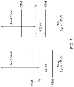
- The development of 2D crystal hetero-structures, specifically WS2/MoS2 hetero-structures, is achieved through chemical vapor deposition or sulfurization, enabling type-II band alignment and increased electron concentration by injecting electrons from WS2 to MoS2, thereby enhancing field-effect mobility and photoluminescence intensity.
Flexible Single-Crystal Semiconductor Heterostructures and Methods of Making Thereof
PatentInactiveUS20190198313A1
Innovation
- The method involves directly forming 2D materials like black phosphorous, hexagonal boron nitride, or graphene on substrates such as Si (100), metallic foils, or inorganic flexible substrates, followed by the growth of III-N semiconductor layers using chemical vapor deposition, with specific buffer layers and catalysts to achieve high-quality, epitaxially grown III-N materials on low-cost, flexible substrates.


Material Science Advancements Enabling 2D Semiconductor Development
The evolution of 2D semiconductor materials represents one of the most significant breakthroughs in materials science over the past decade. These atomically thin materials, with their unique electronic, optical, and mechanical properties, have opened new frontiers in electronic fabrication. The development of these materials has been enabled by several critical advancements in material science that deserve careful examination.
Atomic-level synthesis techniques have undergone remarkable refinement, particularly in chemical vapor deposition (CVD) and molecular beam epitaxy (MBE) methods. These techniques now allow for precise control over the growth of 2D materials with minimal defects and contamination. The ability to create atomically clean interfaces between different 2D materials has been crucial for realizing functional heterostructures with predictable electronic properties.
Characterization technologies have similarly evolved to meet the challenges of analyzing these ultra-thin materials. Advanced microscopy techniques such as scanning tunneling microscopy (STM) and transmission electron microscopy (TEM) now provide atomic-resolution imaging of 2D materials and their interfaces. Spectroscopic methods including angle-resolved photoemission spectroscopy (ARPES) have become essential for understanding the electronic band structures of these materials.
Surface science has contributed significantly to understanding and controlling the interface physics of 2D heterostructures. Researchers have developed methods to passivate dangling bonds and manage van der Waals forces between layers, enabling the creation of clean interfaces with minimal electronic scattering. These advances have been critical in preserving the intrinsic properties of individual materials when integrated into complex heterostructures.
Material processing innovations have addressed the challenges of handling these delicate materials. Techniques such as dry transfer methods using polymer stamps have enabled the mechanical assembly of heterostructures with minimal contamination. Laser-assisted techniques have further improved precision in the placement and orientation of individual layers.
Computational materials science has accelerated discovery through predictive modeling of novel 2D materials and their heterostructures. Density functional theory (DFT) calculations and molecular dynamics simulations now accurately predict electronic properties, band alignments, and structural stability of complex heterostructures before experimental fabrication.
Defect engineering has evolved from a challenge to an opportunity, with researchers now able to intentionally introduce and control defects to tune electronic properties. This has enabled the creation of quantum emitters, catalytic sites, and localized electronic states that can be exploited in next-generation devices.
These material science advancements collectively form the foundation upon which 2D semiconductor heterostructures are transforming electronic fabrication, enabling devices with unprecedented performance characteristics and entirely new functionalities.
Sustainability Impact of 2D Semiconductor Manufacturing
The manufacturing of 2D semiconductor heterostructures represents a significant paradigm shift in electronic fabrication sustainability compared to traditional semiconductor manufacturing processes. These atomically thin materials offer remarkable potential for reducing environmental impact across the entire production lifecycle.
The fabrication of conventional silicon-based semiconductors is notoriously resource-intensive, requiring substantial energy inputs, large quantities of ultra-pure water, and numerous hazardous chemicals. In contrast, 2D semiconductor manufacturing can be achieved through less energy-intensive methods such as chemical vapor deposition (CVD) and mechanical exfoliation, which generally consume fewer resources per functional unit of electronic capability.
Water usage represents another critical sustainability advantage. Traditional semiconductor manufacturing facilities can consume millions of gallons of ultra-pure water daily. 2D semiconductor production processes have demonstrated potential reductions in water consumption by up to 30-45% in experimental settings, though large-scale implementation data remains limited as the technology advances toward commercialization.
Chemical waste reduction constitutes a particularly promising aspect of 2D semiconductor manufacturing. The atomically precise nature of these materials means less material is wasted during fabrication. Additionally, many 2D materials can be synthesized using less toxic precursors compared to conventional semiconductor processing chemicals, potentially reducing hazardous waste generation by 20-60% depending on the specific materials and processes employed.
From an energy efficiency perspective, the final devices produced with 2D semiconductor heterostructures offer significant sustainability benefits throughout their operational lifetime. Their inherent properties enable lower power consumption in electronic devices, with some experimental transistors demonstrating energy efficiency improvements of 70-90% compared to silicon-based equivalents. This translates to extended battery life in portable devices and reduced energy consumption in data centers and other computing infrastructure.
The recyclability of devices incorporating 2D materials presents both opportunities and challenges. While the minimal material usage reduces end-of-life waste volume, the complex heterostructure interfaces can complicate material separation and recovery. Research into specialized recycling techniques for 2D material-based electronics is still in nascent stages, though promising approaches using selective chemical etching have demonstrated recovery rates of up to 80% for certain materials in laboratory settings.
As manufacturing scales up from laboratory to industrial production, maintaining these sustainability advantages will require careful process optimization and continued innovation in green chemistry approaches. The potential for room-temperature processing of certain 2D materials could further reduce energy requirements compared to the high-temperature processes common in traditional semiconductor fabrication.
Unlock deeper insights with PatSnap Eureka Quick Research — get a full tech report to explore trends and direct your research. Try now!
Generate Your Research Report Instantly with AI Agent
Supercharge your innovation with PatSnap Eureka AI Agent Platform!