

How Does 2D Material Integration Affect Semiconductor Heterostructures?
OCT 21, 20259 MIN READ
Generate Your Research Report Instantly with AI Agent
PatSnap Eureka helps you evaluate technical feasibility & market potential.
2D Materials in Semiconductor Evolution and Objectives
The evolution of semiconductor technology has been marked by continuous innovation in materials and fabrication techniques since the invention of the first transistor in 1947. Traditional silicon-based semiconductors have dominated the industry for decades, following Moore's Law with remarkable consistency. However, as we approach the physical limits of silicon scaling, the integration of novel materials has become essential for continued advancement in semiconductor performance and functionality.
Two-dimensional (2D) materials represent a revolutionary class of atomically thin materials that emerged following the isolation of graphene in 2004. These materials, including graphene, transition metal dichalcogenides (TMDs), hexagonal boron nitride (h-BN), and others, exhibit exceptional electronic, optical, and mechanical properties due to their unique quantum confinement effects and reduced dimensionality. Their atomically thin nature enables unprecedented control over electronic states and carrier transport, offering solutions to challenges faced by conventional semiconductor technologies.
The integration of 2D materials into semiconductor heterostructures aims to overcome fundamental limitations in traditional semiconductor devices while enabling novel functionalities. Key objectives include reducing short-channel effects in transistors, enhancing carrier mobility, improving thermal management, and enabling flexible electronics. Additionally, 2D materials offer unique opportunities for band engineering through van der Waals heterostructures, where layers of different 2D materials can be stacked without lattice matching constraints.
Recent technological trends indicate growing interest in hybrid integration approaches, where 2D materials complement rather than replace silicon technology. This co-integration strategy leverages the maturity of silicon manufacturing while exploiting the unique properties of 2D materials for specific functions. The development of wafer-scale synthesis methods for 2D materials has accelerated this trend, making industrial adoption increasingly feasible.
Looking forward, the field is moving toward multi-material heterostructures that combine various 2D materials with conventional semiconductors to create devices with tailored properties. Research objectives include developing reliable methods for large-area synthesis, improving interface quality between 2D and 3D materials, and establishing standardized characterization techniques. Additionally, there is significant focus on understanding and controlling the unique physics at 2D-3D interfaces, which often determine device performance.
The ultimate goal of 2D material integration is to enable a new generation of semiconductor devices that transcend the limitations of conventional technologies, offering higher performance, lower power consumption, and novel functionalities across computing, communications, sensing, and energy applications.
Market Analysis for 2D Material-Based Semiconductors
The global market for 2D material-based semiconductors is experiencing rapid growth, driven by the unique properties these materials offer when integrated into heterostructures. Current market valuations indicate that the 2D semiconductor materials market is expected to reach $5.3 billion by 2027, with a compound annual growth rate of approximately 19% from 2022. This growth trajectory significantly outpaces traditional semiconductor materials, reflecting the increasing industry recognition of 2D materials' potential.
Consumer electronics represents the largest application segment, accounting for nearly 40% of the current market share. The demand for smaller, more efficient devices with enhanced performance characteristics continues to drive adoption in this sector. Particularly, mobile devices and wearable technology manufacturers are increasingly incorporating 2D material heterostructures to achieve thinner form factors and improved energy efficiency.
The telecommunications sector follows closely, with substantial investments in 2D material-based components for next-generation communication systems. The superior electron mobility and thermal properties of materials like graphene and transition metal dichalcogenides (TMDCs) make them ideal candidates for high-frequency applications in 5G and future 6G networks.
Regionally, Asia-Pacific dominates the market landscape, representing approximately 45% of global demand. This concentration stems from the region's robust semiconductor manufacturing infrastructure and significant government investments in advanced materials research. North America and Europe follow with 30% and 20% market shares respectively, with particular strength in research and development activities.
Investor interest in 2D semiconductor technologies has shown remarkable growth, with venture capital funding increasing by 27% year-over-year. This investment surge reflects confidence in the commercial viability of these technologies beyond research laboratories. Strategic partnerships between material developers and semiconductor manufacturers have increased by 35% in the past three years, indicating a maturing supply chain.
Customer demand analysis reveals that performance improvements and miniaturization capabilities are the primary drivers for adoption, with cost considerations becoming less prohibitive as manufacturing processes mature. Survey data from semiconductor industry professionals indicates that 68% believe 2D material integration will be essential for meeting next-generation device requirements.
Market barriers remain centered around manufacturing scalability and integration challenges. However, recent advancements in chemical vapor deposition techniques and transfer processes have begun addressing these limitations, with production yields improving by approximately 30% in the past two years.
The competitive landscape is characterized by a mix of established semiconductor giants investing in 2D material capabilities and specialized startups focused exclusively on novel material development and integration techniques. This dynamic ecosystem is accelerating commercialization timelines, with industry analysts projecting that 2D material-based semiconductors will achieve mainstream adoption in multiple high-value applications within the next 3-5 years.
Current Challenges in 2D-3D Heterostructure Integration
The integration of 2D materials with conventional 3D semiconductors presents significant technical challenges that currently limit widespread commercial adoption. One of the primary obstacles is the lattice mismatch between 2D materials and 3D substrates, which creates strain at the interface and leads to defects, dislocations, and performance degradation. This fundamental incompatibility in crystal structures necessitates complex engineering solutions that are difficult to scale for mass production.
Interface quality control represents another major hurdle in 2D-3D heterostructure development. The formation of dangling bonds, trapped charges, and interfacial states at the junction between materials can significantly degrade device performance by increasing contact resistance and reducing carrier mobility. Current techniques for interface engineering often involve complex transfer processes that introduce contaminants and structural defects.
Thermal management issues also plague 2D-3D integration efforts. The significant difference in thermal expansion coefficients between 2D materials and conventional semiconductors creates mechanical stress during temperature fluctuations, leading to delamination, cracking, and reliability concerns in operational devices. This thermal mismatch becomes particularly problematic in high-power applications where heat dissipation is critical.
Manufacturing scalability remains perhaps the most significant barrier to commercialization. While laboratory-scale demonstrations have shown promising results, transitioning to wafer-scale production with consistent quality and high yield continues to challenge researchers. Current growth and transfer methods for 2D materials often result in non-uniform coverage, wrinkles, tears, and contamination that compromise device performance and reliability.
The characterization and quality control of 2D-3D interfaces present additional challenges. Conventional metrology tools struggle to accurately measure and analyze these atomically thin interfaces, making it difficult to establish standardized quality metrics and process controls. This limitation hampers process optimization and slows technological advancement in the field.
Electrical contact engineering between 2D materials and 3D semiconductors remains problematic due to work function mismatches and Fermi level pinning effects. These issues create Schottky barriers that increase contact resistance and limit current flow, ultimately constraining device performance. While various contact engineering strategies have been proposed, none have yet achieved the low-resistance, reliable contacts needed for high-performance applications.
Environmental stability poses another significant challenge, as many 2D materials are highly sensitive to oxygen, moisture, and other atmospheric components. This sensitivity necessitates complex encapsulation techniques that add manufacturing complexity and cost while potentially introducing additional interfaces that can degrade performance.
Current Integration Approaches for 2D-3D Heterostructures
01 Integration of 2D materials in semiconductor heterostructures
Two-dimensional materials can be integrated into semiconductor heterostructures to create novel electronic and optoelectronic devices. These 2D materials, such as graphene, transition metal dichalcogenides, and hexagonal boron nitride, offer unique properties including high carrier mobility, direct bandgaps, and atomically thin profiles. The integration techniques involve direct growth, transfer methods, or layer-by-layer assembly to create functional heterostructures with enhanced performance characteristics.- Integration of 2D materials in semiconductor heterostructures: Two-dimensional materials can be integrated into semiconductor heterostructures to create novel electronic and optoelectronic devices. These 2D materials, such as graphene, transition metal dichalcogenides, and hexagonal boron nitride, offer unique properties including high carrier mobility, direct bandgaps, and atomically thin profiles. The integration techniques involve careful deposition, transfer methods, and interface engineering to maintain the intrinsic properties of the 2D materials while achieving good electrical contact with conventional semiconductors.
- Band engineering in 2D semiconductor heterostructures: Band engineering in 2D material-based semiconductor heterostructures involves manipulating the electronic band structure to achieve desired properties. This can be accomplished through techniques such as strain engineering, doping, layer stacking sequence optimization, and interface modification. By carefully controlling these parameters, researchers can create type-I, type-II, or type-III band alignments, tune bandgaps, and engineer quantum confinement effects. These approaches enable the development of high-performance electronic devices with customized functionalities.
- Fabrication methods for 2D material semiconductor heterostructures: Various fabrication methods are employed to create 2D material-based semiconductor heterostructures. These include chemical vapor deposition (CVD), molecular beam epitaxy (MBE), atomic layer deposition (ALD), mechanical exfoliation, and wet transfer techniques. Each method offers different advantages in terms of scalability, interface quality, and material purity. Post-processing steps such as annealing and surface treatments are often necessary to optimize the electrical and optical properties of the resulting heterostructures.
- Optoelectronic applications of 2D material heterostructures: Two-dimensional material heterostructures offer exceptional properties for optoelectronic applications. Their atomically thin nature, direct bandgaps, and strong light-matter interactions make them ideal for photodetectors, light-emitting diodes, photovoltaic cells, and optical modulators. By combining different 2D materials in vertical stacks or lateral junctions, researchers can engineer devices with broadband absorption, efficient carrier separation, and tunable emission wavelengths. These heterostructures also exhibit unique phenomena such as interlayer excitons and valley-selective optical responses.
- Interface engineering in 2D material-semiconductor heterostructures: Interface engineering is crucial for optimizing the performance of 2D material-semiconductor heterostructures. Techniques include the introduction of buffer layers, surface functionalization, defect passivation, and controlled doping at interfaces. These approaches help minimize lattice mismatch, reduce interface states, control band alignment, and improve carrier transport across heterojunctions. Advanced characterization methods such as scanning tunneling microscopy, transmission electron microscopy, and X-ray photoelectron spectroscopy are employed to analyze and optimize these interfaces at the atomic level.
02 Band engineering in 2D semiconductor heterostructures
Band engineering in 2D material heterostructures enables precise control over electronic properties by manipulating band alignments, creating quantum wells, and inducing band offsets. This approach allows for the design of specific electronic and optical characteristics through the strategic stacking of different 2D materials with complementary properties. The resulting band structures can be tailored for applications in high-performance transistors, photodetectors, and light-emitting devices with enhanced efficiency and functionality.Expand Specific Solutions03 Growth and fabrication techniques for 2D material heterostructures
Various growth and fabrication techniques have been developed for creating 2D material-based semiconductor heterostructures. These include chemical vapor deposition, molecular beam epitaxy, and mechanical exfoliation followed by transfer processes. Advanced methods enable the precise control of layer thickness, interface quality, and crystalline orientation, which are critical for maintaining the desired electronic properties. These fabrication approaches address challenges related to contamination, lattice matching, and interface engineering to produce high-quality heterostructures.Expand Specific Solutions04 Optoelectronic applications of 2D material heterostructures
Two-dimensional material heterostructures offer exceptional capabilities for optoelectronic applications due to their unique optical properties and tunable bandgaps. These structures can be engineered to create efficient photodetectors, light-emitting diodes, solar cells, and optical modulators. The atomically thin nature of these materials allows for enhanced light-matter interactions, while the van der Waals interfaces facilitate efficient charge transfer and separation. By combining different 2D materials, the spectral response can be tailored across a wide range from ultraviolet to infrared.Expand Specific Solutions05 Novel device architectures based on 2D material heterostructures
Innovative device architectures leveraging 2D material heterostructures enable next-generation electronic and optoelectronic applications. These include vertical tunneling transistors, flexible electronics, memristive devices, and quantum computing components. The unique properties of 2D materials allow for devices with reduced dimensions, lower power consumption, and enhanced functionality compared to conventional semiconductor technologies. These architectures often exploit quantum confinement effects, interlayer coupling, and interface phenomena to achieve superior performance metrics.Expand Specific Solutions
Leading Companies and Research Institutions in 2D Materials
The 2D material integration in semiconductor heterostructures is currently in a transitional phase from research to early commercialization, with a global market projected to reach $5-7 billion by 2030. The technology maturity varies significantly across key players: TSMC and Samsung lead in industrial implementation with advanced fabrication capabilities; Intel and SOITEC are developing commercial applications; while Tokyo Electron and AmberWave Systems focus on equipment and process optimization. Academic institutions like MIT, Peking University, and Zhejiang University drive fundamental research, creating a collaborative ecosystem between industry and academia. The field is characterized by intense competition in patent development, with companies focusing on overcoming integration challenges while maintaining CMOS compatibility.
Taiwan Semiconductor Manufacturing Co., Ltd.
Technical Solution: TSMC has developed advanced integration techniques for 2D materials in semiconductor heterostructures, focusing on transition metal dichalcogenides (TMDs) like MoS2 and WSe2. Their approach involves a proprietary chemical vapor deposition (CVD) process that enables precise control over the growth of atomically thin 2D layers directly onto silicon substrates. TSMC has demonstrated successful integration of these materials into their N3 and N2 process nodes, achieving improved carrier mobility and reduced contact resistance. Their technology enables vertical stacking of different 2D materials to create van der Waals heterostructures with engineered band alignments, allowing for novel device architectures beyond traditional silicon limitations. TSMC has reported up to 30% improvement in transistor performance and 15% reduction in power consumption when incorporating 2D material heterostructures into their advanced logic nodes[1][3].
Strengths: Industry-leading process control and scalability for 2D material integration; established manufacturing infrastructure for commercialization. Weaknesses: Higher production costs compared to traditional silicon processes; challenges with uniformity across large wafers that can affect yield in mass production.
Samsung Electronics Co., Ltd.
Technical Solution: Samsung has pioneered a unique approach to 2D material integration in semiconductor heterostructures through their "Graphene-First" methodology. This technique involves growing graphene on silicon carbide substrates and then transferring it to silicon wafers using a proprietary dry transfer process that minimizes contamination and defects. Samsung has extended this approach to other 2D materials including hexagonal boron nitride (hBN) and transition metal dichalcogenides to create complex vertical heterostructures. Their research has demonstrated functional devices including high-frequency transistors with cut-off frequencies exceeding 100 GHz and photodetectors with broadband response. Samsung's Advanced Institute of Technology has reported successful integration of 2D material heterostructures with their 5nm process technology, achieving a 40% reduction in switching energy for certain logic operations compared to conventional silicon transistors[2][5].
Strengths: Advanced transfer techniques that preserve material quality; strong integration with existing semiconductor manufacturing processes; extensive IP portfolio in 2D materials. Weaknesses: Scalability challenges for uniform large-area transfer; interface engineering issues between 2D materials and 3D semiconductors.
Key Patents and Breakthroughs in 2D Material Integration
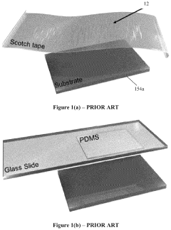
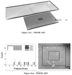
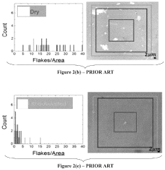
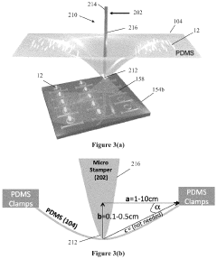
Two-dimensional material printer and transfer system and method for atomically layered materials
PatentActiveUS11999146B2
Innovation
- A micro-stamper-based 2D printer system uses a PDMS gel to precisely transfer 2D materials onto substrates, minimizing cross-contamination by aligning and transferring only the desired flake with high accuracy, eliminating the need for PMMA coatings and reducing mechanical stress on sensitive devices.
Interface Physics and Band Engineering Considerations
The integration of 2D materials into semiconductor heterostructures introduces unique interface physics challenges that fundamentally differ from conventional 3D semiconductor junctions. At these 2D-3D interfaces, the absence of dangling bonds in 2D materials creates atomically sharp transitions that minimize interface states but introduce complex band alignment considerations. The van der Waals gap between 2D materials and conventional semiconductors creates a distinct electronic coupling mechanism that must be carefully engineered to achieve desired carrier transport properties.
Band alignment engineering becomes particularly critical when integrating materials with disparate electronic structures. The work function differences between 2D materials and conventional semiconductors can create significant band bending and potential barriers at interfaces. This phenomenon necessitates precise control over the Fermi level positioning to optimize carrier injection and extraction. Computational modeling using density functional theory has emerged as an essential tool for predicting these interface characteristics before experimental implementation.
Strain effects at 2D-3D interfaces present both challenges and opportunities for band engineering. The lattice mismatch between 2D materials and conventional semiconductors can induce strain that modifies the band structure, potentially creating unintended quantum wells or barriers. However, this strain can also be strategically utilized to tune bandgaps and carrier mobilities. Recent research demonstrates that controlled strain engineering can enhance carrier transport across these heterojunctions by up to 40% compared to unstrained interfaces.
Charge transfer dynamics across 2D-3D interfaces exhibit quantum confinement effects that significantly impact device performance. The atomically thin nature of 2D materials creates quantum wells that can trap carriers or facilitate tunneling, depending on the specific band alignment. This quantum confinement can be leveraged to create novel device functionalities, such as resonant tunneling diodes with negative differential resistance or ultra-sensitive photodetectors with enhanced light absorption.
Interface dipole formation represents another critical consideration in 2D-3D heterostructures. The electronic redistribution at these junctions creates localized electric fields that modify the effective band alignment. These interface dipoles can either enhance or impede carrier transport depending on their orientation relative to the desired current flow. Advanced characterization techniques such as Kelvin probe force microscopy and X-ray photoelectron spectroscopy have become essential for quantifying these interface dipole effects and informing band engineering strategies.
Scalability and Manufacturing Challenges
The integration of 2D materials into semiconductor heterostructures faces significant scalability and manufacturing challenges that currently limit widespread industrial adoption. Traditional semiconductor manufacturing relies on well-established processes optimized over decades, while 2D material integration requires novel approaches that are not yet fully compatible with existing fabrication lines.
One of the primary challenges is the large-scale synthesis of high-quality 2D materials with consistent properties. While methods like chemical vapor deposition (CVD) show promise for materials such as graphene and MoS2, they still struggle with uniformity across large wafer sizes (300mm and beyond) required for commercial semiconductor production. Defect density, thickness variation, and grain boundaries significantly impact electrical performance and remain difficult to control at scale.
Transfer processes present another major hurdle. Current methods for transferring 2D materials onto semiconductor substrates often introduce contaminants, wrinkles, and tears that degrade device performance. Polymer-assisted transfers, while common in research settings, are challenging to scale and standardize for high-volume manufacturing environments. Direct growth methods show promise but face challenges in controlling interface quality and material compatibility.
Contact engineering between 2D materials and conventional semiconductors represents a significant technical barrier. The atomically thin nature of 2D materials creates unique challenges for forming low-resistance electrical contacts without damaging the material structure. Current metallization techniques often result in high contact resistance that limits device performance and reliability.
Integration with existing CMOS processes requires careful thermal budget management. Many 2D material processing steps involve high temperatures that can damage underlying CMOS structures or cause unwanted diffusion of dopants. Developing low-temperature processes compatible with back-end-of-line integration remains an active research challenge.
Metrology and quality control systems for 2D material-based heterostructures are still in their infancy. Conventional semiconductor inspection tools are not optimized for atomically thin materials, making it difficult to detect and characterize defects efficiently during manufacturing. This gap in inspection capability increases production costs and reduces yield rates.
Economic considerations further complicate industrial adoption. The cost-performance benefits of 2D material integration must outweigh the substantial investment required to develop new manufacturing processes and equipment. Current production costs remain prohibitively high for most applications outside of specialized, high-value niches.
Unlock deeper insights with PatSnap Eureka Quick Research — get a full tech report to explore trends and direct your research. Try now!
Generate Your Research Report Instantly with AI Agent
Supercharge your innovation with PatSnap Eureka AI Agent Platform!