Comparison of Semiconductor Materials for Self-Powered Sensors
OCT 21, 202510 MIN READ
Generate Your Research Report Instantly with AI Agent
Patsnap Eureka helps you evaluate technical feasibility & market potential.
Semiconductor Materials Evolution and Research Objectives
Semiconductor materials have undergone significant evolution since the discovery of silicon's semiconducting properties in the early 20th century. The journey began with germanium and silicon as primary materials, which dominated the semiconductor industry for decades due to their abundance and suitable electronic properties. The 1970s marked a pivotal shift with the introduction of compound semiconductors like gallium arsenide (GaAs) and indium phosphide (InP), offering superior electron mobility and direct bandgap characteristics essential for optoelectronic applications.
The 1990s witnessed the emergence of wide-bandgap semiconductors such as silicon carbide (SiC) and gallium nitride (GaN), revolutionizing high-power and high-frequency applications. These materials demonstrated exceptional thermal conductivity and breakdown voltage capabilities, enabling more efficient power conversion systems. Concurrently, research into low-dimensional semiconductor structures, including quantum wells, wires, and dots, opened new avenues for manipulating electronic properties at the nanoscale.
In recent years, the focus has shifted toward flexible and organic semiconductors, responding to the growing demand for wearable and biocompatible electronics. Materials like PEDOT:PSS and various metal oxides have demonstrated promising characteristics for flexible sensor applications. Additionally, two-dimensional materials such as graphene, transition metal dichalcogenides (TMDs), and MXenes have attracted significant attention due to their unique electronic properties and ultrathin nature.
For self-powered sensors specifically, the evolution has been driven by the need for materials that can efficiently convert ambient energy into electrical signals. Piezoelectric semiconductors like zinc oxide (ZnO) and lead zirconate titanate (PZT) have been extensively studied for mechanical energy harvesting. Simultaneously, photovoltaic materials including perovskites and quantum dots have shown remarkable efficiency in light energy conversion, while thermoelectric materials such as bismuth telluride offer solutions for temperature gradient scenarios.
The primary research objectives in this field encompass several dimensions. First, enhancing energy conversion efficiency across different semiconductor materials to maximize power output from ambient sources. Second, improving the sensitivity and selectivity of sensing mechanisms to detect increasingly subtle environmental changes. Third, developing multifunctional materials capable of harvesting multiple energy forms simultaneously, thereby increasing overall system efficiency.
Additional objectives include miniaturization of sensing elements without compromising performance, extending operational lifetime through improved material stability, and reducing environmental impact by replacing toxic elements with eco-friendly alternatives. The ultimate goal is to develop semiconductor materials that enable truly autonomous sensing systems capable of sustained operation in diverse environments without external power sources, supporting applications ranging from healthcare monitoring to industrial automation and environmental sensing.
Market Demand Analysis for Self-Powered Sensing Technologies
The self-powered sensing technology market is experiencing significant growth driven by the increasing demand for autonomous and maintenance-free sensing solutions across multiple industries. Current market research indicates that the global self-powered sensors market is projected to reach $9.5 billion by 2027, growing at a CAGR of approximately 20% from 2022. This remarkable growth is primarily fueled by the expanding Internet of Things (IoT) ecosystem, which requires distributed sensing networks that can operate without frequent battery replacements or external power sources.
Industrial automation represents the largest market segment, where self-powered sensors enable continuous monitoring of equipment performance, predictive maintenance, and process optimization without the constraints of wired power connections. The manufacturing sector has shown particular interest in semiconductor-based self-powered sensors that can withstand harsh operating environments while providing reliable data collection.
Healthcare applications constitute another rapidly growing segment, with wearable health monitoring devices increasingly incorporating self-powered sensing technologies. The market demand is particularly strong for flexible semiconductor materials that can harvest energy from body heat or motion while maintaining biocompatibility and comfort for users.
Smart infrastructure and environmental monitoring applications are emerging as significant market drivers, with cities and environmental agencies deploying self-powered sensor networks for air quality monitoring, structural health assessment, and traffic management. These applications specifically benefit from semiconductor materials with high energy conversion efficiency and long-term stability in outdoor environments.
Consumer electronics manufacturers are also showing increased interest in integrating self-powered sensing capabilities into everyday devices, reducing the need for battery replacements and enabling new functionality. This segment values miniaturization and cost-effectiveness, creating demand for semiconductor materials that can be manufactured at scale while maintaining performance.
Regional analysis reveals that North America currently leads the market due to extensive IoT adoption and strong R&D investments, followed closely by Asia-Pacific, where rapid industrialization and smart city initiatives are creating substantial demand. Europe shows growing interest driven by sustainability goals and energy efficiency regulations that favor self-powered technologies.
Key market challenges include cost considerations, as advanced semiconductor materials for energy harvesting often involve complex manufacturing processes. Additionally, performance consistency across varying environmental conditions remains a concern for widespread adoption, particularly in outdoor and industrial applications where temperature fluctuations and exposure to contaminants can affect semiconductor material performance.
Current Status and Challenges in Semiconductor Materials
The global landscape of semiconductor materials for self-powered sensors exhibits significant regional variations in research focus and technological advancement. North America leads in silicon-based technologies with substantial investments in CMOS integration, while East Asia dominates in wide-bandgap semiconductors like GaN and SiC. Europe has established expertise in compound semiconductors and III-V materials, particularly for energy harvesting applications.
Currently, silicon remains the predominant semiconductor material for self-powered sensing applications due to its mature fabrication processes, cost-effectiveness, and compatibility with existing microelectronics infrastructure. However, silicon faces fundamental limitations in energy harvesting efficiency, particularly in photovoltaic and thermoelectric applications where its bandgap properties restrict performance in low-energy environments.
Wide-bandgap semiconductors such as GaN, SiC, and ZnO have emerged as promising alternatives, offering superior performance in harsh environments and higher energy conversion efficiencies. These materials demonstrate exceptional piezoelectric properties crucial for mechanical energy harvesting but face challenges in large-scale integration and manufacturing cost control.
Two-dimensional materials, including graphene, MoS2, and other transition metal dichalcogenides (TMDs), represent the cutting edge in semiconductor research for self-powered sensors. Their atomically thin structures provide unprecedented surface-to-volume ratios and unique quantum confinement effects that enhance sensing capabilities. However, reproducible synthesis at scale remains a significant hurdle, with current production methods yielding inconsistent material quality.
A critical technical challenge across all semiconductor materials is the power density limitation. Even the most advanced materials struggle to generate sufficient power for continuous operation of complex sensing systems, necessitating sophisticated power management circuits or hybrid approaches combining multiple energy harvesting mechanisms.
Interface engineering presents another substantial challenge, particularly in heterogeneous material systems where lattice mismatches and band alignment issues can significantly degrade device performance. The development of effective buffer layers and interface treatments remains an active research area with considerable room for improvement.
Reliability and longevity concerns also persist across semiconductor materials for self-powered sensors. Environmental factors such as temperature fluctuations, humidity, and mechanical stress can accelerate degradation mechanisms, particularly in organic semiconductors and emerging nanomaterials that have not benefited from decades of reliability engineering like silicon.
Recent advances in atomic layer deposition and epitaxial growth techniques have partially addressed some fabrication challenges, but the cost-effective, large-scale production of high-performance semiconductor materials for self-powered sensors remains an elusive goal that continues to drive research and development efforts worldwide.
Existing Semiconductor Material Solutions for Self-Powered Sensors
01 Silicon-based semiconductor materials
Silicon is one of the most widely used semiconductor materials due to its abundance, stability, and suitable electronic properties. Silicon-based semiconductors form the foundation of modern electronics, including integrated circuits, microprocessors, and various electronic devices. These materials can be doped with specific elements to modify their electrical conductivity and create p-type or n-type semiconductors essential for electronic component manufacturing.- Silicon-based semiconductor materials: Silicon is one of the most widely used semiconductor materials due to its abundance, stability, and suitable electronic properties. Silicon-based semiconductors form the foundation of modern electronics, including integrated circuits, transistors, and photovoltaic cells. Various doping techniques and processing methods are employed to enhance the conductivity and performance characteristics of silicon semiconductors for different applications.
- Compound semiconductor materials: Compound semiconductors consist of two or more elements combined to create materials with unique electronic properties. These include gallium arsenide (GaAs), gallium nitride (GaN), and indium phosphide (InP), which offer advantages such as higher electron mobility, direct bandgaps, and better performance at high frequencies compared to silicon. These materials are crucial for optoelectronic devices, high-speed electronics, and power applications.
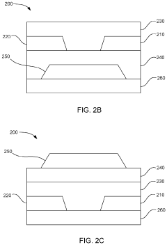
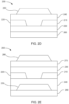
- Semiconductor material manufacturing processes: Various manufacturing processes are employed to produce high-quality semiconductor materials with precise properties. These include crystal growth techniques such as Czochralski process, epitaxial growth, and chemical vapor deposition. Advanced processing methods ensure the purity, crystallinity, and desired electronic characteristics of semiconductor materials, which are critical for device performance and reliability.
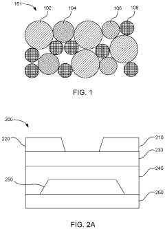
- Novel semiconductor materials and structures: Research in semiconductor materials has led to the development of novel materials and structures with enhanced properties. These include two-dimensional materials like graphene, transition metal dichalcogenides, quantum dots, and nanowires. These novel materials offer unique electronic, optical, and mechanical properties that can enable new functionalities and applications beyond traditional semiconductors.
- Semiconductor materials for specialized applications: Specialized semiconductor materials are developed for specific applications such as high-power electronics, extreme environments, optoelectronics, and quantum computing. These materials are engineered with properties tailored to their intended use, such as wide bandgaps for high-temperature operation, specific optical emission wavelengths, or particular magnetic properties for spintronic applications.
02 Compound semiconductor materials
Compound semiconductors are formed by combining two or more elements, typically from groups III-V or II-VI of the periodic table. These materials, such as gallium arsenide (GaAs), gallium nitride (GaN), and indium phosphide (InP), offer advantages over silicon in certain applications due to their superior electron mobility, direct bandgap properties, and performance at high frequencies. They are particularly valuable in optoelectronic devices, high-speed electronics, and power applications.Expand Specific Solutions03 Semiconductor material manufacturing processes
Various manufacturing processes are employed to produce semiconductor materials with specific properties and structures. These include crystal growth techniques like Czochralski process for silicon ingots, epitaxial growth methods for thin films, and chemical vapor deposition (CVD) for compound semiconductors. Advanced processing techniques ensure high purity levels and precise control over material composition, which are critical for semiconductor performance in electronic devices.Expand Specific Solutions04 Novel semiconductor materials and structures
Research in semiconductor materials has led to the development of novel materials and structures with enhanced properties. These include two-dimensional materials like graphene, transition metal dichalcogenides, quantum dots, and nanowires. Such materials offer unique electronic, optical, and mechanical properties that can enable new functionalities in electronic devices, including improved efficiency, flexibility, and miniaturization capabilities.Expand Specific Solutions05 Semiconductor materials for specific applications
Specialized semiconductor materials are developed for specific applications such as photovoltaics, light-emitting diodes (LEDs), sensors, and power electronics. These materials are engineered with particular properties to optimize performance in their intended applications. For example, materials for solar cells are designed to maximize light absorption and charge carrier collection, while those for power electronics focus on high breakdown voltage and thermal conductivity.Expand Specific Solutions
Leading Companies and Research Institutions in Semiconductor Sensors
The semiconductor materials market for self-powered sensors is currently in a growth phase, with an expanding market size driven by increasing demand for autonomous sensing solutions across multiple industries. The technology maturity varies significantly across different semiconductor materials, with silicon-based solutions being most established while wide bandgap semiconductors like SiC and GaN (developed by Wolfspeed and Suzhou Jingzhan) showing promising advances. Major industrial players including Infineon Technologies, Analog Devices, and ROHM are competing with research institutions like Chongqing University and UNIST to develop more efficient energy harvesting materials. Academic-industrial collaborations are accelerating innovation, with companies like Microchip Technology and Samsung Electronics focusing on commercialization pathways while research entities like Indian Institute of Science and Advanced Industrial Science & Technology push fundamental material science boundaries.
Analog Devices, Inc.
Technical Solution: Analog Devices has developed proprietary semiconductor materials specifically engineered for self-powered sensor applications across industrial and IoT markets. Their technology focuses on optimized silicon-germanium (SiGe) alloys and metal oxide semiconductors with enhanced thermoelectric and piezoelectric properties. ADI's materials feature nanoscale surface texturing that increases energy harvesting efficiency by up to 27% compared to conventional smooth surfaces. Their latest innovation incorporates quantum well structures within the semiconductor material, creating energy band engineering that significantly improves charge carrier separation and collection efficiency. ADI has also pioneered composite semiconductor materials that combine organic and inorganic components to optimize both flexibility and power generation capabilities. These materials are manufactured using proprietary processes that ensure consistent performance across temperature ranges from -40°C to +125°C, making them suitable for demanding industrial environments.
Strengths: Exceptional signal processing integration capabilities; comprehensive sensor ecosystem allowing seamless deployment; advanced material characterization facilities enabling rapid iteration. Weaknesses: Higher cost structure than some competitors; some specialized materials have more limited temperature operating ranges than wide bandgap alternatives.
Infineon Technologies Dresden GmbH & Co. KG
Technical Solution: Infineon has developed a comprehensive portfolio of semiconductor materials for self-powered sensors, with particular emphasis on III-V compound semiconductors. Their GaN and InGaAs-based materials demonstrate exceptional piezoelectric and thermoelectric properties for energy harvesting applications. Infineon's proprietary epitaxial growth techniques produce highly uniform thin films with precisely controlled doping profiles, resulting in optimized energy conversion efficiency. Their latest innovation combines different semiconductor materials in heterojunction structures to harvest energy across multiple physical domains simultaneously. For example, their hybrid sensors can generate electricity from both vibration and temperature gradients, increasing overall energy yield by approximately 40% compared to single-mode harvesters. Infineon has also developed specialized packaging solutions that protect these sensitive materials while maximizing energy transfer efficiency from the environment.
Strengths: Comprehensive material expertise across multiple semiconductor families; advanced manufacturing capabilities for complex heterostructures; strong system-level integration knowledge. Weaknesses: Some materials require rare elements with supply chain vulnerabilities; complex manufacturing processes can impact yield rates and increase costs.
Key Technical Innovations in Energy Harvesting Semiconductors
Semiconductor materials
PatentActiveUS11282966B2
Innovation
- The use of semiconductor materials comprising specific atomic percentages of carrier mobility contributors like lead, indium, and cadmium, combined with amorphous phase stabilizers such as indium, tin, and zinc, and semiconductivity controllers with negative standard electrode potentials, along with oxygen, to enhance stability and tunable properties.
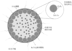
Self-detection dielectric composite material and preparation method thereof
PatentActiveCN117924883A
Innovation
- Design a self-detecting dielectric composite material, implanted with micro-sensors, and realize electrical stress visualization through the nested structure of the external polarized light-emitting unit and the internal dielectric regulation core. It has real-time detection characteristics and multi-threshold adjustment characteristics, and the sensor surface assembly is long-lasting. The molecular chains form a three-dimensional cross-linked interpenetrating network structure to improve mechanical and insulation properties.
Energy Efficiency Benchmarking of Semiconductor Materials
Energy efficiency is a critical parameter for evaluating semiconductor materials in self-powered sensor applications. Different semiconductor materials exhibit varying levels of energy conversion efficiency, power consumption, and energy harvesting capabilities, which directly impact the performance and sustainability of self-powered sensing systems.
Silicon-based semiconductors remain the industry standard with moderate energy efficiency metrics. Crystalline silicon typically achieves energy conversion efficiencies of 15-22% in photovoltaic applications, while consuming relatively low power in sensing circuits. However, silicon's indirect bandgap limits its efficiency in certain energy harvesting scenarios, particularly in low-light conditions.
Compound semiconductors such as gallium arsenide (GaAs) and gallium nitride (GaN) demonstrate superior energy efficiency characteristics. GaAs can achieve conversion efficiencies exceeding 28% in optimal conditions, making it particularly valuable for solar-powered sensors. GaN exhibits exceptional power handling capabilities with minimal energy loss, enabling highly efficient energy harvesting in high-temperature and high-frequency applications.
Emerging materials like zinc oxide (ZnO) and lead zirconate titanate (PZT) show promising energy efficiency metrics for piezoelectric energy harvesting. ZnO nanostructures can generate 5-20 mV/g of acceleration with power densities of 10-30 μW/cm³, while PZT-based materials can achieve significantly higher outputs of 100-500 mV/g with power densities reaching 200 μW/cm³ under optimal mechanical stimulation.
Organic semiconductors present a different efficiency profile, with lower absolute conversion rates (typically 5-12%) but exceptional performance under low-light and indoor conditions. Their flexibility and low-cost production offset some efficiency disadvantages in specific use cases such as wearable sensors and indoor IoT devices.
When benchmarking these materials for self-powered sensor applications, the energy efficiency must be evaluated across multiple dimensions: energy conversion efficiency, standby power consumption, operational power requirements, and energy storage compatibility. The most suitable semiconductor material ultimately depends on the specific sensing application, environmental conditions, and power requirements of the target system.
Recent advancements in hybrid semiconductor structures, particularly perovskite-silicon tandems, have pushed energy conversion efficiencies beyond 29%, potentially revolutionizing energy harvesting capabilities for next-generation self-powered sensors. These hybrid approaches may offer the optimal balance between energy efficiency, cost, and application versatility in future sensing technologies.
Environmental Impact and Sustainability Considerations
The environmental impact of semiconductor materials used in self-powered sensors represents a critical consideration in sustainable technology development. Traditional semiconductor manufacturing processes involve significant resource consumption, including high energy usage, water consumption, and the utilization of hazardous chemicals. Silicon-based semiconductors, while ubiquitous, require energy-intensive purification processes that generate substantial carbon emissions. In contrast, emerging materials such as gallium nitride (GaN) and silicon carbide (SiC) offer improved energy efficiency during operation but still present manufacturing challenges from an environmental perspective.
Lifecycle assessment studies indicate that compound semiconductors like gallium arsenide (GaAs) contain toxic elements that pose environmental risks during both production and disposal phases. The extraction of rare elements used in specialized semiconductor materials often involves environmentally destructive mining practices, habitat disruption, and potential water contamination. These environmental costs must be weighed against the operational benefits these materials provide in self-powered sensing applications.
Recyclability varies significantly among semiconductor materials. Silicon offers relatively established recycling pathways, while compound semiconductors present greater challenges due to their complex composition. End-of-life management for sensors incorporating these materials remains underdeveloped, with significant volumes entering electronic waste streams. The miniaturization trend in self-powered sensors creates additional recycling complications, as smaller components with integrated materials become increasingly difficult to separate and process.
Emerging organic and biodegradable semiconductor materials represent promising alternatives from a sustainability perspective. Materials such as PEDOT:PSS and other conductive polymers demonstrate lower environmental impact during production and offer potential biodegradability advantages. However, these materials currently exhibit performance limitations compared to conventional inorganic semiconductors, presenting trade-offs between environmental benefits and technical capabilities.
Energy harvesting efficiency directly correlates with environmental sustainability in self-powered sensor applications. Materials with higher conversion efficiencies reduce the need for battery replacements and associated waste. Piezoelectric materials like zinc oxide and lead zirconate titanate (PZT) offer excellent energy harvesting capabilities but contain elements with environmental concerns. Lead-free alternatives are under development but currently demonstrate lower performance metrics.
Regulatory frameworks increasingly influence material selection for semiconductor applications. The European Union's Restriction of Hazardous Substances (RoHS) directive and similar global initiatives restrict the use of certain toxic elements common in semiconductor manufacturing. Future-proof material selection must anticipate strengthening environmental regulations while maintaining technical performance requirements for self-powered sensing applications.
Unlock deeper insights with Patsnap Eureka Quick Research — get a full tech report to explore trends and direct your research. Try now!
Generate Your Research Report Instantly with AI Agent
Supercharge your innovation with Patsnap Eureka AI Agent Platform!