Comparison of transparent conductive films based on ITO versus graphene
SEP 24, 20259 MIN READ
Generate Your Research Report Instantly with AI Agent
Patsnap Eureka helps you evaluate technical feasibility & market potential.
TCF Technology Background and Objectives
Transparent conductive films (TCFs) represent a critical component in modern optoelectronic devices, enabling the combination of electrical conductivity with optical transparency. The evolution of TCF technology spans several decades, beginning with the development of indium tin oxide (ITO) in the 1950s. ITO quickly established itself as the industry standard due to its excellent balance of transparency and conductivity, achieving over 90% transparency with sheet resistance below 100 Ω/sq. This performance profile made ITO essential for applications ranging from liquid crystal displays to touch panels and solar cells.
The technological landscape began shifting significantly in the early 2000s with the isolation of graphene, a single-atom-thick carbon sheet with remarkable electrical, optical, and mechanical properties. This breakthrough initiated a new trajectory in TCF development, challenging the long-standing dominance of ITO. The emergence of graphene as a potential alternative coincided with growing concerns about indium scarcity, price volatility, and the inherent brittleness of ITO films that limits their application in flexible electronics.
Current technological trends indicate a progressive transition toward more sustainable, flexible, and cost-effective TCF solutions. While ITO remains the predominant commercial solution with well-established manufacturing processes, graphene-based alternatives are rapidly advancing through research and development phases. The performance metrics for next-generation TCFs increasingly emphasize flexibility, environmental sustainability, and compatibility with large-area, high-throughput manufacturing processes.
The primary technical objectives in this field include achieving sheet resistance below 50 Ω/sq while maintaining optical transparency above 90% in the visible spectrum. Additionally, there is a strong focus on developing TCFs that can withstand mechanical deformation with minimal performance degradation, enabling applications in wearable electronics and flexible displays. Cost reduction represents another critical objective, particularly for graphene-based solutions that currently face economic barriers to widespread adoption.
Research efforts are increasingly directed toward hybrid approaches that combine the advantages of traditional TCF materials with emerging nanomaterials. These include graphene-metal nanowire composites, graphene-conductive polymer hybrids, and multilayer structures that optimize the interface between different materials to enhance overall performance. The ultimate goal is to develop TCF technologies that not only match but exceed the performance of conventional ITO while offering additional functionalities such as flexibility, stretchability, and environmental stability.
The technological trajectory suggests that while complete replacement of ITO may not occur in the immediate future, specialized applications will increasingly adopt graphene-based alternatives where their unique properties provide compelling advantages. This transition will likely accelerate as manufacturing processes mature and production costs decrease, potentially reshaping the TCF landscape within the next decade.
Market Demand Analysis for Transparent Conductors
The transparent conductive film market has witnessed substantial growth in recent years, driven primarily by the expanding electronics industry. The global market for transparent conductors was valued at approximately $5.1 billion in 2022 and is projected to reach $7.8 billion by 2028, growing at a CAGR of 7.3% during the forecast period. This growth trajectory is underpinned by increasing demand for touchscreen devices, smart displays, and photovoltaic applications.
Consumer electronics represent the largest application segment, accounting for over 40% of the market share. The proliferation of smartphones, tablets, and wearable devices has significantly boosted demand for high-performance transparent conductive materials. Additionally, the automotive sector is emerging as a rapidly growing segment, with increasing integration of touch panels and displays in vehicle interiors.
The photovoltaic industry presents another substantial market opportunity, particularly for graphene-based transparent conductors. As solar energy adoption accelerates globally, the demand for more efficient and cost-effective transparent electrodes continues to rise. Industry analysts predict that solar applications could represent 25% of the transparent conductor market by 2030.
Regional analysis reveals that Asia-Pacific dominates the market, accounting for approximately 65% of global production and consumption. This dominance is attributed to the concentration of electronics manufacturing facilities in countries like China, South Korea, Japan, and Taiwan. North America and Europe follow, with growing demand driven by advancements in automotive electronics and renewable energy sectors.
The market exhibits distinct preferences based on application requirements. While ITO remains the incumbent technology with approximately 70% market share due to its established manufacturing ecosystem, graphene-based solutions are gaining traction in premium and specialized applications where flexibility and durability are paramount. Market research indicates that graphene transparent conductors could capture up to 15% market share by 2027.
End-user feedback highlights evolving requirements across different sectors. Display manufacturers prioritize optical transparency (>90%) and low sheet resistance (<100 Ω/sq), while the emerging flexible electronics segment demands materials with excellent mechanical properties under repeated bending conditions. Cost sensitivity varies significantly across applications, with consumer electronics manufacturers showing greater price elasticity compared to specialized industrial or military applications.
The market landscape is further shaped by sustainability considerations, with increasing regulatory pressure to reduce indium usage due to its scarcity and environmental impact. This trend favors alternative materials like graphene, which offer potential advantages in terms of resource sustainability and end-of-life recyclability.
ITO vs Graphene: Current Status and Challenges
The global transparent conductive film (TCF) market is currently dominated by Indium Tin Oxide (ITO), which has been the industry standard for decades. ITO films exhibit excellent optical transparency (>90%) and low sheet resistance (<100 Ω/sq), making them ideal for applications in touch screens, displays, and photovoltaic cells. However, ITO faces significant challenges that have accelerated the search for alternatives, with graphene emerging as a promising contender.
The primary limitation of ITO is the scarcity of indium, which has led to price volatility and supply chain concerns. The global indium reserve is estimated at only 15,000 tons, with China controlling approximately 73% of worldwide production. This geopolitical concentration presents strategic vulnerabilities for manufacturers outside Asia. Additionally, ITO's inherent brittleness severely limits its application in flexible electronics, a rapidly growing market segment projected to reach $48 billion by 2025.
Graphene has emerged as a compelling alternative due to its exceptional electrical conductivity, optical transparency, and mechanical flexibility. Current graphene-based TCFs can achieve sheet resistance of approximately 30-300 Ω/sq with transparency of 80-90%. While these specifications approach ITO performance, consistency in large-scale production remains challenging. The primary methods for graphene TCF production include chemical vapor deposition (CVD), reduced graphene oxide, and liquid-phase exfoliation, each with distinct advantages and limitations.
The geographical distribution of technological development shows interesting patterns. Asia, particularly South Korea and China, leads in ITO production and application, while graphene research centers are more globally distributed, with significant activities in Europe (particularly the UK and Spain), North America, and increasingly in Asia. The EU's Graphene Flagship initiative and similar programs in the UK, US, and China have accelerated graphene TCF development through substantial funding.
Technical challenges for graphene TCFs include achieving uniform large-area deposition, reducing production costs, and improving stability under environmental stresses. Current production costs for graphene TCFs remain 3-5 times higher than ITO, primarily due to immature manufacturing processes. Additionally, graphene TCFs often exhibit degradation when exposed to humidity and certain chemicals, requiring effective encapsulation solutions.
Industry adoption faces further obstacles including integration with existing manufacturing infrastructure, which is heavily optimized for ITO. The transition to graphene-based TCFs would require significant retooling and process adjustments, creating inertia against adoption despite graphene's technical advantages. This highlights the complex interplay between technical capabilities and practical implementation challenges in the evolving landscape of transparent conductive materials.
Current Technical Solutions for ITO and Graphene TCFs
01 ITO film composition and manufacturing methods
Indium Tin Oxide (ITO) films are widely used as transparent conductive films due to their excellent combination of optical transparency and electrical conductivity. Various manufacturing methods and compositions have been developed to optimize these properties. The films typically contain indium oxide doped with tin oxide in specific ratios to achieve the desired conductivity while maintaining high transparency in the visible light spectrum. Manufacturing processes include sputtering, chemical vapor deposition, and sol-gel methods, each offering different advantages in terms of film quality and production efficiency.- ITO film composition and manufacturing methods: Indium Tin Oxide (ITO) films are widely used as transparent conductive films due to their excellent combination of optical transparency and electrical conductivity. Various manufacturing methods have been developed to optimize these properties, including sputtering, chemical vapor deposition, and sol-gel processes. The composition typically includes indium oxide doped with tin at specific ratios to achieve the desired conductivity while maintaining high transparency in the visible light spectrum.
- Graphene-based transparent conductive films: Graphene has emerged as a promising alternative to ITO for transparent conductive films due to its exceptional electrical conductivity, optical transparency, and mechanical flexibility. These films are typically produced through chemical vapor deposition, reduction of graphene oxide, or exfoliation methods. The single-atom thickness of graphene allows for high transparency while its unique electronic structure provides excellent conductivity, making it suitable for various applications including touchscreens, solar cells, and flexible electronics.
- Hybrid and composite transparent conductive materials: Hybrid and composite materials combining different conductive elements offer enhanced performance characteristics compared to single-material films. These composites often incorporate graphene with metal nanowires, carbon nanotubes, or ITO to achieve synergistic effects. The resulting films demonstrate improved conductivity, transparency, and mechanical properties, addressing limitations of individual materials while maintaining high optical transmittance and electrical conductivity required for advanced electronic applications.
- Surface treatment and modification techniques: Various surface treatment and modification techniques are employed to enhance the performance of transparent conductive films. These include plasma treatment, chemical functionalization, and the application of interfacial layers. Such modifications can improve adhesion, reduce surface resistance, enhance optical properties, and increase environmental stability. These treatments are crucial for optimizing the transparency-conductivity balance and extending the lifetime of the films in various applications.
- Application-specific optimization methods: Transparent conductive films can be specifically optimized for different applications such as touch panels, displays, solar cells, and flexible electronics. These optimization methods involve adjusting thickness, composition, deposition parameters, and post-processing techniques to meet specific requirements. For touch panels, emphasis may be placed on response time and durability, while solar cell applications might prioritize specific wavelength transmittance and sheet resistance values to maximize energy conversion efficiency.
02 Graphene-based transparent conductive films
Graphene has emerged as a promising alternative to ITO for transparent conductive films due to its exceptional electrical conductivity, optical transparency, and mechanical flexibility. Single or few-layer graphene films can achieve high transparency (>90%) while maintaining excellent conductivity. Various methods for producing graphene films include chemical vapor deposition, reduced graphene oxide, and transfer techniques. The conductivity of graphene films can be further enhanced through doping or by creating hybrid structures with other conductive materials while preserving their transparency.Expand Specific Solutions03 Hybrid and composite transparent conductive materials
Hybrid and composite materials combining different conductive components offer enhanced performance compared to single-material films. These include ITO-graphene composites, metal nanowire networks embedded in conductive polymers, and carbon nanotube-graphene hybrids. Such combinations can overcome the limitations of individual materials, providing improved flexibility, conductivity, and transparency. The synergistic effects between different components allow for tunable properties to meet specific application requirements while maintaining high optical transparency and electrical conductivity.Expand Specific Solutions04 Surface treatment and modification techniques
Various surface treatment and modification techniques are employed to enhance the performance of transparent conductive films. These include plasma treatment, chemical functionalization, and the application of anti-reflection coatings. Such modifications can improve adhesion between layers, reduce surface resistance, enhance light transmission, and provide protection against environmental degradation. Techniques like controlled etching and patterning can also optimize the balance between transparency and conductivity by creating specific micro or nanostructures on the film surface.Expand Specific Solutions05 Flexible transparent conductive films for next-generation devices
Flexible transparent conductive films are essential for next-generation electronic devices such as foldable displays, wearable electronics, and flexible solar cells. These films require not only high transparency and conductivity but also mechanical flexibility and durability under repeated bending or stretching. Advanced materials and fabrication techniques have been developed to create films that maintain their electrical and optical properties under mechanical stress. Strategies include using inherently flexible materials like graphene, employing special substrate treatments, and developing novel composite structures with strain-resistant properties.Expand Specific Solutions
Key Industry Players in TCF Manufacturing
The transparent conductive film market is currently in a transitional phase, with ITO (Indium Tin Oxide) dominating as the mature technology while graphene emerges as a promising alternative. The global market size is projected to reach $8.46 billion by 2026, growing at 9.2% CAGR. ITO technology, championed by established players like BOE Technology, TCL China Star, and Sony, offers proven reliability but faces challenges of brittleness and indium scarcity. Meanwhile, graphene-based films, being developed by companies like Nitto Denko, Resonac, and research institutions including National University of Singapore and University of California, offer superior flexibility, transparency, and conductivity. However, graphene solutions still face scalability and cost challenges despite their potential to revolutionize flexible electronics applications.
Hitachi Ltd.
Technical Solution: Hitachi has developed comprehensive solutions for both ITO and graphene-based transparent conductive films. Their ITO technology utilizes a high-density plasma sputtering process that creates films with sheet resistance as low as 8 ohms/sq while maintaining transparency above 85%. For applications requiring flexibility, Hitachi has pioneered a nanostructured ITO formulation that can withstand bending to a radius of 10mm without significant performance degradation. In the graphene domain, Hitachi employs a modified chemical vapor deposition technique that produces high-quality graphene films with controlled layer thickness. Their graphene TCFs achieve sheet resistance of approximately 400 ohms/sq with transparency exceeding 96%. Hitachi has developed a proprietary chemical doping method that enhances graphene's conductivity by up to 40% without compromising optical properties. The company has successfully integrated graphene TCFs into prototype touch sensors and display panels, demonstrating stable performance in environmental testing. Hitachi has also explored multilayer architectures combining graphene with metal nanowires to achieve enhanced conductivity while maintaining flexibility.
Strengths: Hitachi's graphene TCFs offer superior environmental stability compared to ITO, with minimal degradation under humidity and temperature cycling. Their chemical doping approach effectively addresses graphene's inherent conductivity limitations. Weaknesses: Graphene TCFs still face challenges in achieving the low sheet resistance needed for large-area displays without compromising transparency, and production costs remain higher than established ITO manufacturing.
Sony Group Corp.
Technical Solution: Sony has pioneered innovative approaches to transparent conductive films, developing both advanced ITO formulations and graphene-based alternatives. Their ITO technology utilizes a specialized low-temperature deposition process that creates highly uniform films with sheet resistance of 15-20 ohms/sq while maintaining over 88% transparency. This process significantly reduces the brittleness typically associated with ITO. For graphene-based TCFs, Sony employs a proprietary roll-to-roll CVD process that enables continuous production of large-area graphene films. Their graphene TCFs achieve sheet resistance of approximately 350 ohms/sq with transparency exceeding 95%. Sony has developed a unique doping technique that enhances graphene's conductivity without compromising transparency. The company has successfully demonstrated graphene TCFs in prototype flexible OLED displays and touch panels, showing stable performance after 100,000+ bending cycles at a 5mm radius. Sony has also explored hybrid structures combining ultrathin ITO with graphene to leverage the advantages of both materials.
Strengths: Sony's graphene TCFs demonstrate exceptional mechanical durability and flexibility, with minimal performance degradation under repeated bending. Their roll-to-roll production approach offers potential for scaled manufacturing. Weaknesses: Production costs for graphene TCFs remain significantly higher than ITO alternatives, and achieving consistently low sheet resistance across large areas continues to be challenging.
Critical Patents and Innovations in TCF Technology
Transparent Conducting Film and Manufacturing Method of The Same
PatentActiveKR1020130134893A
Innovation
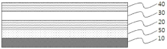
- A multilayer ITO structure comprising a first and third layer with high SnO2 content and a second layer with low SnO2 content, acting as a crystallization seed, allows for low sheet resistance without increasing crystallization temperature, achieved by forming layers with specific SnO2 content ratios and a possible undercoating layer for improved optical properties.
Patent
Innovation
- Development of graphene-based transparent conductive films with comparable or superior conductivity to ITO while maintaining high optical transparency, offering a flexible and mechanically robust alternative.
- Implementation of cost-effective and scalable manufacturing processes for graphene TCFs, such as roll-to-roll production, that can compete economically with established ITO manufacturing.
- Integration of graphene TCFs into flexible and stretchable electronic devices where ITO's brittleness is a limitation, enabling new form factors and applications.
Environmental Impact and Sustainability Considerations
The environmental impact of transparent conductive films (TCFs) has become increasingly important as electronics manufacturers face growing pressure to adopt sustainable practices. ITO (Indium Tin Oxide), the industry standard for decades, presents significant environmental concerns throughout its lifecycle. Indium mining is particularly problematic, causing habitat destruction, soil contamination, and water pollution. The extraction process is energy-intensive and often occurs in regions with limited environmental regulations, leading to substantial ecological damage.
Manufacturing ITO films requires high-temperature processes that consume considerable energy, contributing to carbon emissions. The etching processes used in ITO production typically involve hazardous chemicals such as hydrochloric acid and nitric acid, which can cause environmental harm if not properly managed. Additionally, the scarcity of indium as a resource raises sustainability concerns about long-term viability.
Graphene-based TCFs offer a promising alternative from an environmental perspective. The carbon-based nature of graphene means it can be derived from abundant and renewable resources. Production methods such as chemical vapor deposition (CVD) and solution processing can be optimized to reduce energy consumption compared to ITO manufacturing. Notably, graphene films can be produced at lower temperatures, potentially reducing the carbon footprint of manufacturing processes.
Waste management represents another critical difference between these technologies. ITO waste contains heavy metals that require specialized disposal procedures to prevent environmental contamination. In contrast, graphene waste management presents fewer hazardous material concerns, though nanomaterial safety protocols must still be observed during production and disposal.
Life cycle assessment (LCA) studies comparing ITO and graphene TCFs indicate that graphene solutions could reduce environmental impact by 50-70% when considering factors such as global warming potential, resource depletion, and ecotoxicity. However, these benefits depend heavily on the specific graphene production method employed, as some approaches remain energy-intensive.
Recyclability further differentiates these materials. ITO recycling processes are complex and often economically unfeasible, resulting in significant electronic waste. Graphene-based films show greater potential for recycling and recovery, particularly when integrated into circular economy frameworks. Some research indicates that graphene can be recovered from devices and repurposed, extending its useful life and reducing resource consumption.
Manufacturing Scalability and Cost Analysis
The manufacturing scalability of transparent conductive films (TCFs) represents a critical factor in their commercial viability. ITO (Indium Tin Oxide) benefits from decades of established manufacturing infrastructure, with mature sputtering and vapor deposition techniques enabling consistent production at industrial scales. Current global ITO production capacity exceeds 1,600 tons annually, supporting a market valued at approximately $3.5 billion. However, ITO manufacturing faces significant limitations including high energy consumption (typically 7-10 kWh per square meter), process temperatures exceeding 300°C, and vacuum requirements that increase capital expenditure and operational costs.
Graphene TCFs present a contrasting manufacturing profile with emerging scalable production methods. Roll-to-roll chemical vapor deposition (CVD) has demonstrated throughput capabilities of up to 5 meters per minute for single-layer graphene, while solution-processing techniques offer even higher theoretical throughput at 20+ meters per minute. These ambient-temperature processes consume substantially less energy, with estimates suggesting 60-70% reduction compared to ITO manufacturing. The elimination of vacuum requirements further reduces capital equipment costs by approximately 40-50%.
Cost analysis reveals ITO's current economic advantage due to scale economies, with production costs ranging from $8-15 per square meter for standard specifications. The primary cost driver remains indium, which accounts for 35-45% of material expenses and faces supply constraints as a rare earth element. Price volatility has seen indium fluctuate between $200-800/kg over the past decade, creating significant cost uncertainties for manufacturers.
Graphene TCF production costs currently range from $20-60 per square meter, with substantial variation based on production method and quality requirements. However, cost projection models indicate potential for graphene TCFs to achieve price parity with ITO within 3-5 years as production scales increase. The primary cost drivers for graphene include catalyst substrates (typically copper foil) and transfer processes, which together represent approximately 60% of current production expenses.
Manufacturing yield presents another critical distinction, with mature ITO processes achieving 85-95% yields in high-volume production. Graphene manufacturing currently demonstrates more variable yields ranging from 60-80%, though rapid improvements have been observed as process optimizations continue. The defect density in commercially produced graphene films has decreased by an order of magnitude over the past five years, suggesting continued yield improvements are achievable through further process refinement and quality control advancements.
Unlock deeper insights with Patsnap Eureka Quick Research — get a full tech report to explore trends and direct your research. Try now!
Generate Your Research Report Instantly with AI Agent
Supercharge your innovation with Patsnap Eureka AI Agent Platform!