What are the key material challenges in transparent conductive films development
SEP 24, 20259 MIN READ
Generate Your Research Report Instantly with AI Agent
Patsnap Eureka helps you evaluate technical feasibility & market potential.
TCF Development Background and Objectives
Transparent conductive films (TCFs) represent a critical component in modern optoelectronic devices, enabling the development of touchscreens, displays, solar cells, and other technologies that require both optical transparency and electrical conductivity. The evolution of TCFs began in the 1930s with the development of tin-doped indium oxide (ITO), which has dominated the market for decades due to its excellent combination of transparency and conductivity.
The technological trajectory of TCFs has been shaped by increasing demands for flexibility, cost reduction, and sustainability. Initially focused on rigid glass substrates, the field has progressively moved toward flexible electronics applications, necessitating materials that maintain performance under mechanical stress. This shift has accelerated research into alternative materials beyond traditional metal oxides.
Current technological trends in TCF development include the exploration of nanomaterials such as carbon nanotubes, graphene, metal nanowires, and conductive polymers. These materials offer potential advantages in flexibility, stretchability, and resource efficiency compared to conventional ITO films. Additionally, hybrid approaches combining multiple materials are emerging as promising strategies to overcome individual material limitations.
The primary technical objectives in TCF development center on achieving an optimal balance between transparency and conductivity while addressing several key challenges. These include enhancing mechanical durability for flexible applications, reducing manufacturing costs, minimizing environmental impact, and ensuring compatibility with existing production infrastructure. Specifically, the industry aims to develop TCFs with sheet resistance below 100 Ω/sq while maintaining optical transparency above 90% in the visible spectrum.
Market pressures are driving TCF innovation toward materials that can be processed at lower temperatures, enabling compatibility with temperature-sensitive substrates such as polymers. Additionally, there is growing interest in developing TCFs through solution-based processing methods that could significantly reduce production costs compared to vacuum-based deposition techniques traditionally used for ITO.
The environmental sustainability of TCF materials has become increasingly important, with particular concern regarding the scarcity and environmental impact of indium mining. This has accelerated research into earth-abundant alternatives that can match or exceed the performance of conventional materials while reducing reliance on critical raw materials.
As we look toward future applications, TCF development is increasingly focused on emerging technologies such as flexible displays, wearable electronics, smart windows, and building-integrated photovoltaics. These applications present unique technical requirements that are shaping research priorities and material development strategies in the field.
Market Analysis for Transparent Conductive Applications
The transparent conductive films (TCF) market has witnessed substantial growth driven by the proliferation of touch-enabled devices across consumer electronics, automotive interfaces, and emerging display technologies. Currently valued at approximately 5.1 billion USD in 2023, the market is projected to reach 8.7 billion USD by 2028, representing a compound annual growth rate of 11.3% during the forecast period.
The consumer electronics segment dominates the TCF market, accounting for over 60% of the total demand. Smartphones and tablets remain the primary application areas, with annual production volumes exceeding 1.5 billion units globally. The increasing adoption of larger display sizes and flexible form factors in premium devices has intensified the demand for high-performance TCFs with enhanced optical and mechanical properties.
Automotive applications represent the fastest-growing segment, with a projected CAGR of 17.2% through 2028. The integration of touch panels in vehicle infotainment systems, heads-up displays, and digital instrument clusters is driving this growth. Premium automotive manufacturers are increasingly incorporating curved and irregularly shaped displays, creating demand for TCFs with superior formability and durability characteristics.
The geographical distribution of TCF demand closely follows electronics manufacturing hubs, with East Asia accounting for approximately 72% of global consumption. China leads with 43% market share, followed by South Korea (16%) and Japan (13%). However, emerging manufacturing centers in Southeast Asia and India are showing accelerated growth rates exceeding 15% annually.
Material-wise, indium tin oxide (ITO) continues to dominate with approximately 68% market share despite material challenges. Alternative technologies including silver nanowires, metal mesh, carbon nanotubes, and PEDOT:PSS collectively represent 32% of the market, with silver nanowire solutions showing the most rapid adoption at 24% annual growth.
Price sensitivity varies significantly across application segments. While consumer electronics manufacturers prioritize cost-effectiveness, automotive and premium device manufacturers demonstrate willingness to pay premium prices for TCFs offering superior performance characteristics. The average selling price for high-end TCFs ranges from 15-25 USD per square meter, while standard-grade materials average 8-12 USD per square meter.
Future market growth will be driven by emerging applications including flexible displays, transparent heaters for autonomous vehicle sensors, transparent antennas for 5G/6G communications, and smart architectural glass. These applications collectively represent a potential additional market of 3.2 billion USD by 2030, contingent upon overcoming current material limitations in flexibility, durability, and cost-effectiveness.
Current Challenges in TCF Material Science
Transparent conductive films (TCFs) face several critical material challenges that impede their widespread adoption across various applications. The most significant obstacle remains the trade-off between optical transparency and electrical conductivity. As film thickness decreases to improve transparency, electrical resistance typically increases, creating an inherent conflict between these two essential properties. This fundamental limitation has driven researchers to explore novel materials and structures beyond traditional indium tin oxide (ITO).
Material cost and scarcity present another major challenge, particularly with ITO-based films. Indium is a rare earth element with limited global reserves, leading to price volatility and supply chain vulnerabilities. The semiconductor and display industries' growing demand for indium further exacerbates this issue, necessitating the development of alternative materials that utilize more abundant elements.
Mechanical flexibility represents a crucial hurdle for next-generation flexible electronics. Conventional TCF materials like ITO are inherently brittle, exhibiting performance degradation or complete failure when subjected to bending or stretching. This limitation severely restricts their application in emerging flexible displays, wearable devices, and conformable solar cells, where mechanical durability under repeated deformation is essential.
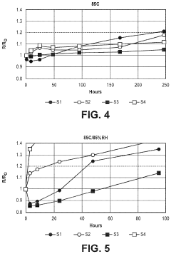
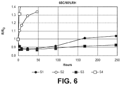
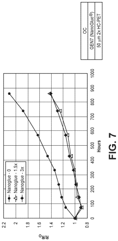
Environmental stability poses significant challenges for many promising TCF materials. Silver nanowire networks and conductive polymers often suffer from oxidation, corrosion, or degradation when exposed to ambient conditions, humidity, or UV radiation. These degradation mechanisms lead to diminished performance over time, reducing device lifespan and reliability in real-world applications.
Manufacturing scalability remains problematic for many novel TCF technologies. While materials like graphene, carbon nanotubes, and metal nanowires show promising performance in laboratory settings, transitioning these to large-scale, cost-effective production processes presents considerable technical difficulties. Uniform deposition over large areas, process reproducibility, and integration with existing manufacturing infrastructure are particularly challenging.
Interface engineering between TCFs and adjacent device layers introduces additional complexity. Contact resistance, work function matching, and adhesion issues can significantly impact overall device performance. These challenges are especially pronounced in multilayer devices like OLEDs, solar cells, and touch panels, where charge transfer across interfaces is critical for device functionality.
Balancing multiple performance parameters simultaneously—including transparency, conductivity, flexibility, stability, and cost—represents perhaps the most formidable challenge in TCF development. Most current solutions excel in one or two aspects but fall short in others, highlighting the need for comprehensive materials engineering approaches that address all critical performance metrics concurrently.
Material cost and scarcity present another major challenge, particularly with ITO-based films. Indium is a rare earth element with limited global reserves, leading to price volatility and supply chain vulnerabilities. The semiconductor and display industries' growing demand for indium further exacerbates this issue, necessitating the development of alternative materials that utilize more abundant elements.
Mechanical flexibility represents a crucial hurdle for next-generation flexible electronics. Conventional TCF materials like ITO are inherently brittle, exhibiting performance degradation or complete failure when subjected to bending or stretching. This limitation severely restricts their application in emerging flexible displays, wearable devices, and conformable solar cells, where mechanical durability under repeated deformation is essential.
Environmental stability poses significant challenges for many promising TCF materials. Silver nanowire networks and conductive polymers often suffer from oxidation, corrosion, or degradation when exposed to ambient conditions, humidity, or UV radiation. These degradation mechanisms lead to diminished performance over time, reducing device lifespan and reliability in real-world applications.
Manufacturing scalability remains problematic for many novel TCF technologies. While materials like graphene, carbon nanotubes, and metal nanowires show promising performance in laboratory settings, transitioning these to large-scale, cost-effective production processes presents considerable technical difficulties. Uniform deposition over large areas, process reproducibility, and integration with existing manufacturing infrastructure are particularly challenging.
Interface engineering between TCFs and adjacent device layers introduces additional complexity. Contact resistance, work function matching, and adhesion issues can significantly impact overall device performance. These challenges are especially pronounced in multilayer devices like OLEDs, solar cells, and touch panels, where charge transfer across interfaces is critical for device functionality.
Balancing multiple performance parameters simultaneously—including transparency, conductivity, flexibility, stability, and cost—represents perhaps the most formidable challenge in TCF development. Most current solutions excel in one or two aspects but fall short in others, highlighting the need for comprehensive materials engineering approaches that address all critical performance metrics concurrently.
Current Material Solutions for TCF Development
01 Carbon nanotube-based transparent conductive films
Carbon nanotubes (CNTs) offer a promising alternative to traditional transparent conductive materials due to their excellent electrical conductivity, mechanical flexibility, and optical transparency. These films can be fabricated through various methods including solution processing and direct growth techniques. The challenges include achieving uniform dispersion, reducing junction resistance between nanotubes, and balancing transparency with conductivity. Recent advancements focus on surface functionalization and hybrid structures to enhance performance.- Carbon nanotube-based transparent conductive films: Carbon nanotubes (CNTs) offer a promising alternative to traditional transparent conductive materials due to their excellent electrical conductivity, mechanical flexibility, and optical transparency. These films can be fabricated through various methods including solution processing and direct growth. The challenge lies in achieving uniform dispersion of CNTs and establishing good contact between individual nanotubes to ensure optimal conductivity while maintaining high transparency.
- Metal nanowire transparent conductors: Metal nanowires, particularly silver nanowires, are emerging as viable materials for transparent conductive films due to their high conductivity and flexibility. These nanowires can be deposited using solution-based processes, making them suitable for large-area applications. Key challenges include improving the adhesion of nanowires to substrates, reducing junction resistance between nanowires, and enhancing environmental stability against oxidation and corrosion while maintaining optical clarity.
- Indium Tin Oxide (ITO) alternatives and limitations: While Indium Tin Oxide (ITO) has been the industry standard for transparent conductive films, its brittleness, limited flexibility, and the scarcity of indium have driven research toward alternatives. The material faces challenges in flexible electronics applications due to crack formation under bending stress. Additionally, the high-temperature processing requirements and increasing cost of indium have accelerated the search for alternative materials that can match ITO's combination of high transparency and conductivity.
- Graphene-based transparent conductive materials: Graphene offers exceptional potential for transparent conductive films due to its theoretical conductivity, optical transparency, and mechanical strength. However, practical challenges include developing scalable production methods that maintain graphene's intrinsic properties, controlling the number of layers to optimize the transparency-conductivity trade-off, and improving the sheet resistance to levels comparable with conventional materials. Doping strategies and hybrid structures are being explored to enhance graphene's performance in transparent electrode applications.
- Conductive polymers and hybrid composite films: Conductive polymers such as PEDOT:PSS and hybrid composites combining organic and inorganic materials offer solutions for flexible transparent electrodes. These materials can be processed at low temperatures using solution-based methods, making them compatible with plastic substrates. The main challenges include improving their electrical conductivity while maintaining high transparency, enhancing environmental stability against moisture and UV degradation, and developing scalable manufacturing processes for uniform film deposition.
02 Metal nanowire transparent conductors
Metal nanowires, particularly silver nanowires, are emerging as viable alternatives for transparent conductive films. These materials offer high conductivity and flexibility while maintaining good optical transparency. The main challenges include long-term stability against oxidation, mechanical durability during bending or stretching, and achieving consistent performance across large areas. Research focuses on protective coatings, embedding techniques, and junction engineering to overcome these limitations.Expand Specific Solutions03 Indium tin oxide (ITO) limitations and alternatives
While indium tin oxide (ITO) has been the industry standard for transparent conductive films, it faces significant challenges including indium scarcity, brittleness limiting flexibility, and high processing temperatures. Various alternative materials are being developed to address these limitations, including doped metal oxides, conductive polymers, and hybrid structures. The key challenge is finding materials that can match ITO's combination of high transparency and low sheet resistance while offering additional benefits like flexibility and lower cost.Expand Specific Solutions04 Graphene-based transparent conductive materials
Graphene offers exceptional potential for transparent conductive films due to its theoretical conductivity, optical transparency, and mechanical properties. However, practical challenges include large-scale production of high-quality graphene, controlling layer numbers, and reducing sheet resistance without compromising transparency. Research focuses on doping strategies, transfer techniques, and hybrid structures combining graphene with other conductive materials to enhance overall performance for applications in flexible electronics and optoelectronic devices.Expand Specific Solutions05 Conductive polymer composites for flexible transparent electrodes
Conductive polymers like PEDOT:PSS and their composites offer advantages for flexible transparent electrodes including solution processability, mechanical flexibility, and compatibility with roll-to-roll manufacturing. The main challenges include achieving sufficient conductivity, long-term environmental stability, and uniform electrical properties. Recent developments focus on secondary dopants, solvent treatments, and incorporation of nanomaterials to enhance conductivity while maintaining transparency for applications in flexible displays and photovoltaics.Expand Specific Solutions
Leading Companies in TCF Industry
The transparent conductive films (TCF) market is currently in a growth phase, with increasing demand driven by touch screens, displays, and photovoltaic applications. The market is expected to reach significant scale as consumer electronics and renewable energy sectors expand. Technologically, silver nanowire solutions from companies like C3 Nano are challenging traditional indium tin oxide (ITO) dominance. Major players including Sony, Canon, and BOE Technology are advancing material innovations to address key challenges such as flexibility, transparency-conductivity balance, and cost reduction. Japanese corporations like Konica Minolta, TDK, and FUJIFILM lead in high-performance TCF development, while academic institutions like South China University of Technology and Beihang University contribute fundamental research to overcome material limitations.
Sony Group Corp.
Technical Solution: Sony has developed proprietary transparent conductive film technology focusing on hybrid materials that combine the advantages of different conductive systems. Their approach centers on silver nanowire networks embedded in conductive polymer matrices, creating synergistic effects that address key material challenges. Sony's technology employs a specialized deposition process that ensures uniform nanowire distribution and optimal junction formation, achieving sheet resistance below 20 ohms/square while maintaining transparency above 90%. Their films incorporate proprietary surface treatments that enhance environmental stability and adhesion to various substrate materials. Sony has developed specialized encapsulation techniques to protect silver nanowires from oxidation and sulfidation, significantly improving long-term stability. Their manufacturing process is compatible with flexible substrates, enabling applications in foldable displays and wearable electronics. Sony has also pioneered techniques to minimize haze and maximize clarity in their TCFs, addressing optical quality challenges critical for high-end display applications.
Strengths: Excellent balance of optical-electrical properties; superior flexibility for next-generation display applications; good compatibility with existing manufacturing infrastructure; enhanced environmental stability compared to standard silver nanowire films. Weaknesses: Complex manufacturing process requiring precise control of multiple parameters; higher production costs compared to single-material approaches; challenges with scaling to very large area applications; potential for optical interference effects requiring additional engineering solutions.
Heraeus Epurio GmbH
Technical Solution: Heraeus Epurio has developed CLEVIOS™, an advanced family of conductive polymer formulations based on poly(3,4-ethylenedioxythiophene) polystyrene sulfonate (PEDOT:PSS) for transparent conductive film applications. Their technology addresses key material challenges through proprietary formulation techniques that enhance conductivity while maintaining transparency. Heraeus has achieved sheet resistance values below 100 ohms/square with transparency exceeding 90% through specialized secondary doping strategies and post-treatment processes. Their formulations incorporate unique additives that improve film formation, adhesion to various substrates, and environmental stability. Heraeus has developed specialized processing techniques that enable uniform thin film deposition through various methods including slot-die coating, screen printing, and inkjet printing. Their PEDOT:PSS formulations feature tunable work functions, making them suitable for various electronic device architectures, particularly in organic electronics and photovoltaics where energy level matching is critical.
Strengths: Excellent flexibility and stretchability; solution processability at low temperatures; compatibility with roll-to-roll manufacturing; environmentally friendly compared to metal-based alternatives. Weaknesses: Lower conductivity compared to metal-based TCFs; sensitivity to humidity and UV exposure requiring encapsulation; challenges achieving ultra-low sheet resistance needed for large-area applications; limited thermal stability at high temperatures.
Key Innovations in TCF Material Engineering
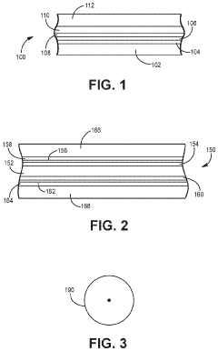
Coatings and processing of transparent conductive films for stabilization of sparse metal conductive layers
PatentPendingUS20240161943A1
Innovation
- A transparent conductive film comprising a sparse metal conductive layer supported by a polymer substrate with a polymer overcoat containing noble metal ions, where the film is processed with heat and optionally humidity to achieve a sheet resistance of no more than 120 ohms/sq and transmittance of at least 88% through the formation of a fused metal nanostructured network.
Transparent conductive film
PatentWO2014167960A1
Innovation
- A transparent conductive film with a substrate and a conductive layer having specific surface roughness parameters (Ra75, Rz, RzJIS94) and containing polythiophene-based resin with controlled particle size and thickness, along with a semimetal film for improved gas barrier properties, to ensure stable conductivity and transparency.
Environmental Impact of TCF Manufacturing
The manufacturing processes of Transparent Conductive Films (TCFs) present significant environmental challenges that warrant careful consideration. Traditional TCF production, particularly those based on indium tin oxide (ITO), involves energy-intensive sputtering processes that consume substantial electricity and generate considerable carbon emissions. The extraction of rare earth elements like indium creates additional environmental burdens through habitat disruption, water pollution, and soil contamination at mining sites. These environmental impacts are exacerbated by the limited global supply of indium, with reserves concentrated primarily in China, leading to geopolitical tensions and sustainability concerns.
Chemical processes in TCF manufacturing often utilize hazardous substances including strong acids, organic solvents, and heavy metals. These chemicals pose risks of air pollution, water contamination, and potential health hazards for workers and surrounding communities. The etching processes employed in patterning TCFs generate toxic waste streams that require specialized treatment and disposal protocols to prevent environmental contamination.
The life cycle assessment of TCFs reveals concerning end-of-life management issues. Most electronic devices containing TCFs are not designed for easy disassembly or material recovery, resulting in significant material loss when these products reach end-of-life. The complex multi-layer structure of many TCFs complicates recycling efforts, with valuable materials often ending up in landfills or being incinerated, releasing harmful substances into the environment.
Recent regulatory developments worldwide are increasingly addressing these environmental concerns. The European Union's Restriction of Hazardous Substances (RoHS) and Registration, Evaluation, Authorization and Restriction of Chemicals (REACH) regulations have placed stricter controls on materials used in electronics manufacturing, including TCFs. Similar regulatory frameworks are emerging in North America and Asia, pushing manufacturers to adopt greener production methods.
In response to these challenges, the industry is exploring more sustainable alternatives. Carbon-based TCFs utilizing graphene and carbon nanotubes offer potentially lower environmental impacts during production and disposal. Metal nanowire networks, particularly those using silver, present another promising direction with manufacturing processes that can be less energy-intensive than traditional methods. Water-based production techniques are gradually replacing solvent-based processes, reducing volatile organic compound emissions and improving workplace safety profiles.
Supply Chain Considerations for Critical TCF Materials
The global supply chain for transparent conductive films (TCFs) faces significant vulnerabilities due to the concentration of critical raw materials in specific geographic regions. Indium, essential for ITO (Indium Tin Oxide) production, is primarily sourced from China, which controls approximately 55% of global reserves. This geographic concentration creates substantial supply risks, as evidenced by price volatilities exceeding 300% during past trade tensions.
Material scarcity represents another critical challenge, particularly for rare elements like indium and silver used in nanowire-based TCFs. Current extraction rates suggest potential supply constraints within 15-20 years, necessitating the development of recycling technologies and alternative materials. Recovery rates for indium from end-of-life electronics currently remain below 15%, highlighting significant improvement opportunities.
Processing capabilities for high-purity TCF materials are similarly concentrated, with Japan and South Korea dominating advanced manufacturing techniques for premium-grade films. This specialization creates bottlenecks when demand surges, as witnessed during the 2020-2021 period when lead times extended from 8 weeks to over 20 weeks for specialized TCF variants.
Environmental regulations increasingly impact TCF supply chains, with the EU's REACH regulations and similar frameworks in other regions restricting certain processing chemicals. Manufacturers must navigate complex compliance requirements across different markets, often necessitating region-specific material formulations that complicate global distribution strategies.
Vertical integration strategies are emerging among major TCF producers to mitigate supply risks. Companies like Nitto Denko and 3M have established strategic partnerships with mining operations and material refiners to secure priority access to critical raw materials. This trend is reshaping industry dynamics, potentially disadvantaging smaller manufacturers without similar supply chain control.
Alternative material development offers promising pathways to reduce dependency on scarce resources. Carbon-based TCFs utilizing graphene and carbon nanotubes present lower supply chain risks due to carbon's abundance, though manufacturing scale-up challenges remain. Similarly, metal mesh technologies using aluminum rather than silver could reduce dependency on precious metals, provided technical performance barriers can be overcome.
Just-in-time inventory practices have proven particularly vulnerable in the TCF sector, with the COVID-19 pandemic exposing systemic weaknesses. Industry leaders are now implementing strategic stockpiling of critical materials, typically maintaining 6-12 month reserves of essential components to buffer against supply disruptions.
Unlock deeper insights with Patsnap Eureka Quick Research — get a full tech report to explore trends and direct your research. Try now!
Generate Your Research Report Instantly with AI Agent
Supercharge your innovation with Patsnap Eureka AI Agent Platform!