Transparent conductive films in aerospace communication device integration
SEP 24, 20259 MIN READ
Generate Your Research Report Instantly with AI Agent
Patsnap Eureka helps you evaluate technical feasibility & market potential.
Aerospace TCF Technology Background and Objectives
Transparent conductive films (TCFs) have emerged as a critical enabling technology in aerospace communication systems over the past three decades. Initially developed for consumer electronics displays, these films have evolved significantly to meet the rigorous demands of aerospace applications, where extreme temperatures, radiation exposure, and mechanical stress present unique challenges.
The evolution of TCFs in aerospace began with indium tin oxide (ITO) films in the 1990s, which offered reasonable conductivity and transparency but suffered from brittleness and limited flexibility. As aerospace communication systems advanced toward more integrated and conformal designs, the limitations of traditional TCFs became increasingly apparent, driving innovation toward alternative materials and fabrication methods.
Current aerospace communication systems require TCFs that can maintain performance integrity across temperature ranges from -65°C to +150°C while withstanding vibration, radiation, and vacuum conditions. These films serve multiple functions in modern aerospace communication devices, including electromagnetic interference (EMI) shielding, touch interfaces for control systems, transparent antennas, and solar cell integration for power generation.
The global push toward satellite constellations for broadband internet and advanced defense communication networks has accelerated the demand for specialized TCFs that can be integrated into curved surfaces and complex geometries while maintaining optimal radio frequency (RF) transmission characteristics. This represents a significant shift from earlier applications where optical transparency was the primary concern.
Recent advancements in nanomaterials, particularly carbon nanotubes, graphene, and silver nanowire networks, have opened new possibilities for aerospace TCFs with enhanced durability and performance. These materials offer promising alternatives to traditional ITO, potentially addressing key limitations in flexibility, weight, and radiation resistance.
The primary technical objectives for aerospace TCF development include achieving sheet resistance below 10 ohms/square while maintaining optical transparency above 90% in the relevant wavelength ranges. Additionally, these films must demonstrate mechanical flexibility with minimal performance degradation after 10,000+ bending cycles, resistance to atomic oxygen erosion in low Earth orbit, and compatibility with standard aerospace manufacturing processes.
Long-term goals include developing TCFs capable of self-healing after micrometeoroid impacts, adaptive conductivity in response to changing environmental conditions, and integration with structural health monitoring systems. These advancements would significantly enhance the reliability and functionality of next-generation aerospace communication platforms, particularly for deep space missions and advanced satellite networks.
Market Analysis for Aerospace Communication Devices
The aerospace communication devices market has experienced significant growth over the past decade, driven by increasing satellite deployments, space exploration missions, and the modernization of aircraft communication systems. The global market for aerospace communication equipment was valued at approximately $6.7 billion in 2022 and is projected to reach $9.8 billion by 2028, representing a compound annual growth rate (CAGR) of 6.5%.
Transparent conductive films (TCFs) have emerged as critical components in modern aerospace communication devices, enabling the integration of touch interfaces, displays, and antennas while maintaining optical clarity and electromagnetic performance. The market for TCFs specifically in aerospace applications was estimated at $320 million in 2022, with expectations to grow at 8.2% annually through 2027.
Key market drivers include the rapid expansion of satellite constellations for global internet coverage, with companies like SpaceX, OneWeb, and Amazon's Project Kuiper planning to deploy thousands of satellites in the coming years. Each satellite requires multiple communication systems incorporating TCF technology. Additionally, the commercial aviation sector's demand for enhanced in-flight connectivity and entertainment systems has created substantial opportunities for TCF integration in cabin communication devices.
Military and defense applications represent another significant market segment, with advanced fighter aircraft, unmanned aerial vehicles (UAVs), and military satellites requiring high-performance communication systems that can operate in extreme conditions. This sector values the lightweight, durable, and EMI-shielding properties that advanced TCFs provide.
Regional analysis indicates North America dominates the market with approximately 42% share, followed by Europe (28%) and Asia-Pacific (23%). However, the Asia-Pacific region is experiencing the fastest growth rate at 9.7% annually, driven by China's ambitious space program and increasing defense modernization efforts across the region.
Customer requirements in this market emphasize reliability under extreme temperature fluctuations (-65°C to +150°C), radiation resistance, low weight, flexibility, and compatibility with curved surfaces. Additionally, there is growing demand for TCFs that can provide multiple functions simultaneously, such as combining touch sensitivity with antenna capabilities or integrating solar energy harvesting with communication functions.
Market challenges include the high cost of specialty TCFs designed for aerospace applications, which can be 5-10 times more expensive than consumer electronics equivalents, and the stringent certification requirements that extend product development cycles. Supply chain vulnerabilities have also been exposed during recent global disruptions, with 68% of aerospace manufacturers reporting TCF component shortages affecting production schedules.
Current TCF Technology Status and Challenges
Transparent conductive films (TCFs) have become increasingly critical components in aerospace communication devices, with current global development showing significant regional disparities. North America and Europe lead in advanced TCF research and aerospace applications, while Asia-Pacific countries, particularly China, Japan, and South Korea, dominate in manufacturing capacity and commercial production. This geographical distribution has created complex supply chain dependencies that present strategic challenges for aerospace industries.
The current state-of-the-art TCF technologies primarily revolve around indium tin oxide (ITO), which has maintained market dominance due to its excellent combination of optical transparency (>90%) and electrical conductivity (<100 Ω/sq). However, ITO faces significant limitations in aerospace applications, including brittleness that compromises durability under extreme conditions, limited flexibility that restricts integration with curved surfaces common in aerospace designs, and vulnerability to cosmic radiation that can degrade performance over time.
Alternative TCF materials have emerged to address these challenges, including silver nanowires, carbon nanotubes, graphene, and PEDOT:PSS conductive polymers. While these materials offer improved flexibility and radiation resistance compared to ITO, they still face substantial technical hurdles. Silver nanowires struggle with long-term stability in space environments, carbon nanotubes and graphene encounter scalability and uniformity issues, and conductive polymers typically demonstrate lower conductivity than their inorganic counterparts.
The aerospace sector imposes uniquely stringent requirements on TCFs that exceed those of consumer electronics. These include operational stability across extreme temperature ranges (-150°C to +150°C), resistance to intense radiation exposure, minimal outgassing in vacuum conditions, and exceptional mechanical durability under high vibration and G-forces during launch. Current TCF technologies struggle to simultaneously satisfy all these demanding parameters.
Manufacturing challenges further complicate TCF advancement for aerospace applications. Achieving consistent quality at scale remains problematic, particularly for newer nanomaterial-based films. The specialized deposition techniques required for aerospace-grade TCFs, including advanced sputtering methods and controlled atmosphere processing, significantly increase production costs and limit widespread adoption.
The integration of TCFs with other aerospace communication components presents additional technical barriers. Interface compatibility issues between TCFs and underlying substrates can lead to delamination under thermal cycling, while electromagnetic interference (EMI) shielding requirements often conflict with optical transparency needs. These integration challenges have slowed the implementation of advanced TCF solutions in critical aerospace communication systems.
Current TCF Integration Solutions for Aerospace
01 Carbon nanotube-based transparent conductive films
Carbon nanotubes (CNTs) can be used to create transparent conductive films with excellent electrical conductivity and optical transparency. These films can be fabricated through various methods such as solution processing, vacuum filtration, or direct growth. The CNT networks form conductive pathways while maintaining high transparency, making them suitable for applications in touch screens, displays, and solar cells. The films can be further enhanced by doping or functionalization to improve their conductivity.- Carbon nanotube-based transparent conductive films: Carbon nanotubes (CNTs) can be used to create highly transparent and conductive films. These films exhibit excellent electrical conductivity while maintaining high optical transparency, making them suitable for various electronic applications. The CNTs can be dispersed in solutions and coated onto substrates using methods such as spray coating or vacuum filtration. These films offer advantages such as flexibility, chemical stability, and compatibility with various substrates.
- Metal oxide-based transparent conductive films: Metal oxides, particularly indium tin oxide (ITO), are widely used for transparent conductive films. These materials provide a good balance of optical transparency and electrical conductivity. The films can be deposited using techniques such as sputtering, chemical vapor deposition, or sol-gel methods. Metal oxide films are commonly used in displays, touch screens, and photovoltaic devices. Research focuses on improving their flexibility and finding alternatives to reduce dependence on scarce elements like indium.
- Metal nanowire transparent conductive films: Metal nanowires, particularly silver nanowires, can form networks that create transparent conductive films. These nanowire networks provide conductive pathways while allowing light to pass through the spaces between wires. The films can be fabricated using solution-based processes such as spray coating, spin coating, or roll-to-roll printing. Metal nanowire films offer advantages including high flexibility, stretchability, and potential for low-cost manufacturing compared to traditional transparent conductors.
- Graphene-based transparent conductive films: Graphene, a single layer of carbon atoms arranged in a hexagonal lattice, can be used to create transparent conductive films with exceptional properties. These films exhibit high electrical conductivity, optical transparency, and mechanical flexibility. Graphene films can be produced through methods such as chemical vapor deposition, reduced graphene oxide, or exfoliation techniques. The unique combination of properties makes graphene films promising for applications in flexible electronics, solar cells, and touch screens.
- Hybrid and composite transparent conductive films: Hybrid or composite transparent conductive films combine multiple materials to achieve enhanced performance. These can include combinations of metal nanowires with graphene, carbon nanotubes with conductive polymers, or metal oxides with metallic grids. The synergistic effects of combining different materials can lead to improved conductivity, transparency, flexibility, and stability. These hybrid approaches often aim to overcome the limitations of single-material films while maintaining their advantages for applications in optoelectronic devices.
02 Metal nanowire transparent conductive films
Metal nanowires, particularly silver nanowires, can be used to create highly transparent and conductive films. These nanowires form a percolating network that allows for electrical conductivity while maintaining optical transparency. The films can be fabricated through solution-based processes such as spray coating, spin coating, or roll-to-roll printing. Metal nanowire films offer advantages such as flexibility, stretchability, and compatibility with various substrates, making them suitable for flexible electronics and touch panels.Expand Specific Solutions03 Indium tin oxide (ITO) transparent conductive films
Indium tin oxide (ITO) is a widely used material for transparent conductive films due to its high conductivity and transparency in the visible spectrum. These films are typically deposited using techniques such as sputtering, chemical vapor deposition, or sol-gel methods. ITO films are used in various applications including displays, touch screens, and photovoltaic devices. However, the limited supply and high cost of indium have led to research into alternative materials.Expand Specific Solutions04 Graphene-based transparent conductive films
Graphene, a single layer of carbon atoms arranged in a hexagonal lattice, can be used to create transparent conductive films with exceptional electrical, optical, and mechanical properties. These films can be produced through methods such as chemical vapor deposition, reduced graphene oxide, or exfoliation. Graphene-based films offer advantages such as high flexibility, chemical stability, and potentially lower cost compared to traditional transparent conductors, making them promising for next-generation flexible electronics and optoelectronic devices.Expand Specific Solutions05 Hybrid and composite transparent conductive films
Hybrid or composite transparent conductive films combine different materials to achieve enhanced performance characteristics. These may include combinations of metal nanowires with carbon nanotubes, graphene with metal grids, or conductive polymers with inorganic materials. The synergistic effects of these combinations can lead to improved conductivity, transparency, flexibility, and stability. These hybrid films are particularly useful for applications requiring specific performance metrics that cannot be achieved with single-material films.Expand Specific Solutions
Leading Players in Aerospace TCF Development
The transparent conductive films (TCFs) market in aerospace communication device integration is currently in a growth phase, with increasing demand driven by the need for lightweight, flexible, and high-performance communication systems. The global market size is expanding rapidly, projected to reach significant value as aerospace technologies advance. Technologically, the field shows moderate maturity with ongoing innovation. Leading players include C3 Nano, which has pioneered solution-based silver nanowire technologies as ITO replacements, BOE Technology Group offering advanced display solutions, and Nitto Denko providing specialized optical films. Japanese corporations like Sumitomo Metal Mining and AGC are contributing significant materials expertise, while research institutions such as Industrial Technology Research Institute and Korea Electrotechnology Research Institute are advancing fundamental technologies through collaborative industry partnerships.
AGC, Inc. (Japan)
Technical Solution: AGC has developed a sophisticated transparent conductive film technology specifically engineered for aerospace communication applications. Their proprietary "Fluoro-ITO" combines indium tin oxide with fluorine-doped compounds to create films with exceptional environmental stability. These films achieve sheet resistance of 8-12 ohms/square while maintaining optical transparency above 92% in the critical communication wavelengths. AGC's technology incorporates a multi-layer structure with specialized barrier films that prevent oxygen and moisture penetration, critical for maintaining performance in space environments. Their manufacturing process employs advanced sputtering techniques that create highly uniform films with thickness variations below 2% across large areas, essential for consistent signal transmission in phased array systems. AGC has developed a proprietary surface treatment that enhances adhesion to aerospace-grade substrates while maintaining flexibility for integration onto curved surfaces. Their films demonstrate exceptional thermal stability, maintaining conductivity within 5% of baseline performance through temperature cycling from -150°C to +200°C, making them ideal for satellites and spacecraft communication systems that experience extreme temperature variations.
Strengths: Exceptional optical clarity and uniformity; superior environmental stability in space conditions; excellent adhesion to aerospace substrates; proven reliability in extreme temperature environments. Weaknesses: Higher production costs due to specialized materials and processing; slightly higher sheet resistance compared to some metal nanowire alternatives; limited flexibility compared to polymer-based solutions.
Industrial Technology Research Institute
Technical Solution: The Industrial Technology Research Institute (ITRI) has pioneered a hybrid transparent conductive film technology specifically engineered for aerospace communication systems. Their approach combines graphene with metal mesh structures in a multi-layer configuration that achieves sheet resistance of approximately 5-7 ohms/square while maintaining over 88% optical transparency. ITRI's films feature a specialized anti-reflection coating that enhances signal transmission quality and reduces interference in aerospace communication bands (X, Ku, and Ka). The institute has developed a proprietary roll-to-roll manufacturing process that enables production of large-area films with exceptional uniformity (±3% variation) critical for phased array antennas and radar systems. Their films incorporate self-healing properties through a unique polymer matrix that can repair minor damage from micrometeoroid impacts, extending operational lifespan in space environments. ITRI's technology has been successfully tested under simulated space conditions including thermal cycling (-150°C to +150°C) and vacuum exposure for over 5,000 hours.
Strengths: Exceptional durability in extreme aerospace environments; self-healing capabilities extend operational lifespan; excellent EMI shielding properties; scalable manufacturing process. Weaknesses: Higher production complexity requiring specialized equipment; slightly lower optical transparency compared to some competing technologies; requires specialized bonding techniques for integration with aerospace substrates.
Key Patents and Innovations in Aerospace TCF
Transparent conductive film, electronic device, and method for manufacturing electronic device
PatentWO2012056774A1
Innovation
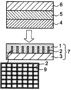
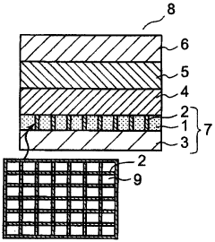
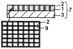
- A transparent conductive film is developed with a conductive layer composed of a water-soluble vinyl polymer, an organic additive, and a conductive organic polymer compound, specifically polyanilines, polypyrroles, or polythiophenes, integrated into the openings of a conductive metal mesh layer on a transparent substrate, optimizing adhesiveness and conductivity.
Method of manufacturing transparent conductive film, the transparent conductive film, element and transparent conductive substrate using the film, as well as device using the substrate
PatentInactiveUS9701849B2
Innovation
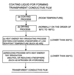
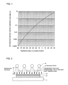
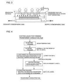
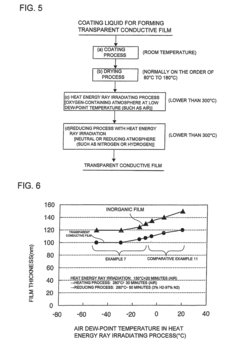
- A method involving a coating process with a liquid containing organic indium, tin, or zinc compounds, followed by energy ray irradiation under an oxygen-containing atmosphere at a low dew-point temperature, which promotes mineralization and densification of the film, forming a densely packed conductive oxide fine-particle layer with improved transparency, conductivity, and strength.
Material Durability in Extreme Aerospace Environments
Transparent conductive films (TCFs) deployed in aerospace communication devices face extraordinary durability challenges due to the extreme conditions encountered in aerospace environments. These materials must withstand temperature fluctuations ranging from -150°C to +150°C during orbital transitions from shadow to direct solar exposure. Such thermal cycling induces significant mechanical stress that can compromise film integrity and conductivity performance over time.
Radiation exposure presents another critical durability concern, with high-energy particles and UV radiation causing progressive degradation of both the conductive and transparent properties of these films. Studies indicate that conventional ITO (Indium Tin Oxide) films experience up to 30% reduction in conductivity after equivalent exposure to one year in low Earth orbit conditions, while newer graphene-based alternatives show improved radiation resistance with only 8-12% degradation under similar conditions.
Atomic oxygen erosion, particularly prevalent in low Earth orbit at altitudes between 180-650 km, aggressively attacks carbon-based materials through oxidation processes. This phenomenon has been documented to erode unprotected carbon nanotube-based TCFs at rates of 3-5 nm per day, necessitating specialized protective coatings that maintain optical transparency while providing chemical resistance.
Mechanical vibration and shock during launch sequences subject TCFs to acceleration forces exceeding 10g, requiring exceptional adhesion between the conductive film and substrate materials. Delamination failures represent approximately 40% of documented TCF failures in aerospace applications, highlighting the importance of interface engineering in film construction.
Vacuum conditions in space environments introduce additional challenges through outgassing phenomena, where volatile components within the film structure evaporate, potentially contaminating sensitive optical equipment and permanently altering film composition. Industry standards now require TCF materials to demonstrate less than 1% total mass loss under standardized outgassing tests (ASTM E595).
Micrometeoroid and orbital debris impacts, though rare, present catastrophic failure risks for exposed TCF surfaces. Current research focuses on self-healing film technologies incorporating microcapsules with conductive repair materials that activate upon impact damage, though these solutions currently sacrifice 15-20% of initial conductivity performance.
Recent advances in material science have yielded promising durability enhancements, including atomic layer deposition techniques for creating ultra-thin protective barriers and hybrid nanocomposite structures that combine the durability advantages of multiple material systems. These innovations have extended projected service lifetimes from 3-5 years to potentially 7-10 years for next-generation aerospace TCF implementations.
Space Qualification Standards for TCF Technologies
Transparent conductive films (TCFs) deployed in aerospace communication systems must adhere to rigorous space qualification standards that far exceed terrestrial requirements. These standards are primarily governed by organizations such as NASA, ESA, JAXA, and military specifications like MIL-STD-810. The qualification process encompasses extensive testing regimes designed to verify TCF performance under extreme space conditions.
Radiation hardness testing represents a critical qualification parameter, as TCFs must maintain conductivity and transparency when exposed to high-energy particles and solar radiation. Standards typically require materials to withstand total ionizing doses of 100 krad to 1 Mrad depending on mission profile and orbital parameters. Vacuum stability testing evaluates outgassing characteristics, with ASTM E595 specifying maximum total mass loss (TML) of less than 1.0% and collected volatile condensable materials (CVCM) below 0.1%.
Thermal cycling qualification subjects TCFs to extreme temperature fluctuations ranging from -150°C to +150°C for low Earth orbit applications, with more demanding requirements for deep space missions. Standards mandate materials maintain performance through hundreds or thousands of cycles without delamination, cracking, or significant changes in electrical conductivity.
Atomic oxygen resistance testing is particularly important for LEO applications, where highly reactive atomic oxygen can rapidly degrade organic materials. Qualification standards require TCFs to demonstrate minimal erosion rates when exposed to AO fluences representative of mission duration, typically measured in atoms/cm².
Mechanical durability standards assess TCF resistance to launch vibration and acoustic loads. Vibration testing follows NASA-STD-7001A protocols, subjecting components to random vibration profiles that simulate launch conditions. Additionally, TCFs must meet strict outgassing requirements to prevent contamination of sensitive optical equipment.
Electromagnetic compatibility testing ensures TCFs do not interfere with communication systems and can withstand electromagnetic interference. Standards like MIL-STD-461 define acceptable emission and susceptibility levels. Finally, accelerated lifetime testing protocols estimate long-term performance, with qualification standards typically requiring TCFs to maintain at least 80% of initial performance metrics after simulated exposure equivalent to the mission duration plus margin.
Unlock deeper insights with Patsnap Eureka Quick Research — get a full tech report to explore trends and direct your research. Try now!
Generate Your Research Report Instantly with AI Agent
Supercharge your innovation with Patsnap Eureka AI Agent Platform!