Why transparent conductive films are critical for next generation OLED displays
SEP 24, 20259 MIN READ
Generate Your Research Report Instantly with AI Agent
Patsnap Eureka helps you evaluate technical feasibility & market potential.
TCF Technology Background and Objectives
Transparent conductive films (TCFs) have evolved significantly since their inception in the early 20th century, transitioning from rudimentary materials to sophisticated components essential for modern display technologies. The journey began with the development of tin-doped indium oxide (ITO) in the 1940s, which revolutionized transparent electronics with its unique combination of optical transparency and electrical conductivity. As display technologies progressed from CRTs to LCDs and now to OLEDs, TCFs have continuously adapted to meet increasingly demanding performance requirements.
The evolution of OLED displays, particularly flexible and foldable variants, has created unprecedented challenges for TCF technology. Traditional rigid TCFs are no longer sufficient for next-generation displays that require both flexibility and durability under repeated mechanical stress. This technological inflection point has spurred intensive research into alternative TCF materials and structures that can maintain performance while accommodating physical deformation.
Current technical objectives for TCF development focus on achieving an optimal balance of seemingly contradictory properties. These include maximizing optical transparency (>90% in the visible spectrum) while maintaining low sheet resistance (<10 ohms/square), ensuring mechanical flexibility with minimal performance degradation after thousands of bending cycles, and developing manufacturing processes that are both economically viable and environmentally sustainable. Additionally, there is a growing emphasis on reducing reliance on scarce materials like indium, which faces supply constraints and price volatility.
The strategic importance of TCF technology extends beyond display applications. As the electronics industry moves toward transparent, flexible, and wearable devices, advanced TCFs will become enabling components for innovations in solar cells, touch sensors, and smart surfaces. This broader applicability has intensified research efforts and investment in TCF development globally, with significant contributions from both academic institutions and industrial R&D centers.
Recent technological breakthroughs, including nanomaterial-based alternatives like silver nanowires, carbon nanotubes, and graphene, have demonstrated promising results in laboratory settings. However, translating these advances into commercially viable products requires overcoming substantial challenges in scalability, long-term stability, and integration with existing manufacturing infrastructure. The technical trajectory suggests a hybrid approach may ultimately prevail, combining the strengths of different materials to achieve performance targets that no single material can deliver independently.
The ultimate goal of current TCF research is to develop solutions that not only enable the next generation of OLED displays but also anticipate future requirements for emerging technologies such as microLED displays, augmented reality interfaces, and transparent electronics. This forward-looking approach ensures that TCF technology will continue to evolve in parallel with the display technologies it enables.
OLED Display Market Demand Analysis
The OLED display market has experienced remarkable growth over the past decade, driven primarily by increasing consumer demand for superior visual experiences across various electronic devices. Market research indicates that the global OLED display market reached approximately $38 billion in 2022 and is projected to grow at a compound annual growth rate (CAGR) of 13.4% through 2028. This growth trajectory underscores the expanding market opportunity for next-generation display technologies that incorporate advanced transparent conductive films.
Consumer electronics, particularly smartphones and premium televisions, represent the largest application segments for OLED displays. The smartphone sector alone accounts for over 60% of the current OLED market, with major manufacturers like Samsung, Apple, and Huawei increasingly adopting OLED technology in their flagship and mid-range devices. This trend is expected to continue as consumers demonstrate willingness to pay premium prices for devices offering superior display quality, color accuracy, and energy efficiency.
Emerging application areas are further expanding market demand for advanced OLED displays. The automotive industry is increasingly incorporating OLED technology in dashboard displays and entertainment systems, with projections suggesting a 25% annual growth rate in this segment. Similarly, wearable technology manufacturers are adopting flexible OLED displays to enable innovative form factors and enhanced user experiences.
Regional analysis reveals that Asia-Pacific dominates the OLED display market, accounting for approximately 70% of global production capacity. South Korea leads manufacturing output, followed by China, which is rapidly expanding its production capabilities through substantial government and private sector investments. North America and Europe represent significant consumer markets but have limited manufacturing presence.
Consumer preference surveys indicate growing demand for specific display characteristics that next-generation OLEDs must address. These include higher resolution (beyond 4K), improved brightness levels, reduced power consumption, and enhanced durability. Additionally, there is increasing market interest in flexible, foldable, and transparent display options, particularly in premium device segments.
The sustainability aspect is becoming increasingly important in market dynamics. Consumers and regulatory bodies are placing greater emphasis on energy-efficient displays and environmentally responsible manufacturing processes. This trend favors OLED technology, which typically offers lower power consumption compared to traditional LCD displays, but also creates pressure for further efficiency improvements in next-generation products.
Price sensitivity analysis reveals that while consumers demonstrate willingness to pay premium prices for advanced display technologies, there exists a critical price threshold beyond which adoption rates decline significantly. This underscores the importance of cost-effective manufacturing processes for transparent conductive films and other key OLED components to enable broader market penetration.
Current TCF Development Status and Challenges
Transparent conductive films (TCFs) have evolved significantly over the past decade, with indium tin oxide (ITO) dominating the market despite its inherent limitations. Currently, ITO accounts for approximately 85% of the global TCF market due to its established manufacturing infrastructure and reliable performance characteristics. However, the industry faces critical challenges as next-generation OLED displays demand increasingly stringent performance metrics that traditional ITO struggles to meet.
The primary technical challenges facing TCF development center around achieving an optimal balance between transparency and conductivity. Current ITO films typically offer 85-90% transparency with sheet resistance of 10-100 ohms/square, which becomes insufficient for larger, flexible OLED panels. Additionally, ITO's brittleness (cracking at bend radii below 8mm) severely limits its application in foldable and rollable displays—a rapidly growing segment of the market.
Material scarcity presents another significant challenge, as indium is classified as a critical raw material with limited global reserves primarily concentrated in China (approximately 50% of world production). This geographic concentration creates supply chain vulnerabilities and price volatility, with indium prices fluctuating by over 30% in recent years.
Manufacturing scalability issues further complicate TCF advancement. Current vacuum deposition methods for ITO are energy-intensive and relatively slow, with limitations in processing speed and substrate compatibility. The industry requires deposition techniques compatible with roll-to-roll manufacturing to achieve the cost efficiencies needed for mass production of next-generation displays.
Alternative TCF technologies have emerged to address these limitations, including silver nanowire networks, carbon nanotubes, graphene, and metal mesh structures. Silver nanowire films have demonstrated promising performance with transparency exceeding 90% and sheet resistance below 10 ohms/square, while maintaining flexibility with bend radii below 1mm. However, these alternatives face their own challenges in long-term stability, uniformity at scale, and integration with existing manufacturing processes.
Regional development patterns show Asia-Pacific dominating TCF production, with South Korea and Japan leading in high-performance TCF research. European efforts focus primarily on sustainable alternatives to ITO, while North American research emphasizes novel nanomaterials and deposition techniques. This geographic distribution of expertise creates both collaboration opportunities and competitive challenges in the global supply chain.
The environmental impact of TCF production represents an additional challenge, with traditional ITO manufacturing processes generating significant waste and consuming substantial energy. Regulatory pressures in key markets are increasingly demanding more sustainable production methods and materials, driving research toward greener alternatives and recycling technologies.
Current TCF Solutions for OLED Applications
01 Carbon nanotube-based transparent conductive films
Carbon nanotubes (CNTs) can be used to create transparent conductive films with excellent electrical conductivity and optical transparency. These films can be fabricated through various methods such as solution processing, vacuum filtration, or direct growth. The unique structure of carbon nanotubes allows for high electron mobility while maintaining transparency, making them suitable for applications in touch screens, displays, and solar cells.- Carbon nanotube-based transparent conductive films: Carbon nanotubes (CNTs) can be used to create transparent conductive films with excellent electrical conductivity and optical transparency. These films can be fabricated through various methods such as solution processing or direct growth. The unique structure of carbon nanotubes allows for high electron mobility while maintaining transparency, making them suitable for applications in touch screens, displays, and solar cells. The conductivity and transparency can be tuned by controlling the density and alignment of the nanotubes.
- Metal oxide transparent conductive films: Metal oxides, particularly indium tin oxide (ITO), are widely used for transparent conductive films due to their combination of high electrical conductivity and optical transparency. These films can be deposited using techniques such as sputtering, chemical vapor deposition, or sol-gel methods. The electrical and optical properties can be optimized by controlling the composition, thickness, and deposition parameters. Alternative metal oxides like zinc oxide, aluminum-doped zinc oxide, and fluorine-doped tin oxide are also being developed to address the scarcity and cost issues associated with indium.
- Silver nanowire transparent conductive films: Silver nanowire networks offer a promising alternative for transparent conductive films with high flexibility. These films consist of randomly distributed silver nanowires that form a conductive network while allowing light to pass through the spaces between wires. The conductivity and transparency can be tuned by adjusting the nanowire density, length, and diameter. Silver nanowire films can be fabricated using solution-based processes such as spray coating, spin coating, or roll-to-roll printing, making them suitable for flexible electronics applications.
- Graphene-based transparent conductive films: Graphene, a single layer of carbon atoms arranged in a hexagonal lattice, can be used to create transparent conductive films with exceptional electrical, optical, and mechanical properties. These films exhibit high electron mobility, excellent transparency, and remarkable flexibility. Various methods can be employed to produce graphene films, including chemical vapor deposition, reduced graphene oxide, and exfoliation techniques. The conductivity and transparency can be enhanced by doping, stacking multiple layers, or creating hybrid structures with other materials.
- Hybrid and composite transparent conductive films: Hybrid and composite transparent conductive films combine different materials to achieve enhanced performance characteristics. These films typically integrate two or more conductive materials such as metal nanowires with graphene, carbon nanotubes with metal oxides, or conductive polymers with metallic grids. The synergistic effects between the components can lead to improved conductivity, transparency, flexibility, and stability. These hybrid structures can overcome the limitations of individual materials and offer tailored properties for specific applications in flexible electronics, solar cells, and touch panels.
02 Metal oxide transparent conductive films
Metal oxides, particularly indium tin oxide (ITO), are widely used as transparent conductive materials. These films offer a good balance between optical transparency and electrical conductivity. Various deposition techniques such as sputtering, chemical vapor deposition, and sol-gel methods can be employed to create these films with controlled thickness and properties. Doping strategies can be used to enhance conductivity while maintaining high transparency.Expand Specific Solutions03 Silver nanowire transparent conductive films
Silver nanowires can form networks that exhibit high transparency and conductivity. These nanowires can be deposited using solution-based processes such as spray coating, spin coating, or roll-to-roll printing, making them suitable for flexible electronics. The aspect ratio of the nanowires and their junction resistance significantly affect the overall performance of the transparent conductive film. Post-treatment methods can be applied to improve conductivity by reducing junction resistance.Expand Specific Solutions04 Graphene-based transparent conductive films
Graphene, a single layer of carbon atoms arranged in a hexagonal lattice, offers exceptional electrical conductivity and optical transparency. Graphene films can be produced through chemical vapor deposition, reduction of graphene oxide, or exfoliation methods. The quality of graphene, including its defect density and layer number, significantly impacts the balance between transparency and conductivity. Various doping strategies can be employed to enhance the conductivity of graphene films.Expand Specific Solutions05 Composite and hybrid transparent conductive films
Composite or hybrid structures combining different conductive materials can achieve enhanced performance by leveraging the advantages of each component. These may include combinations of metal nanowires with graphene, carbon nanotubes with conductive polymers, or metal oxides with metallic grids. Such hybrid approaches can overcome the limitations of individual materials, offering improved mechanical flexibility, stability, and performance. These composite films often exhibit synergistic effects that result in better transparency-conductivity trade-offs.Expand Specific Solutions
Major TCF and OLED Industry Players
Transparent conductive films (TCFs) are emerging as a critical component in next-generation OLED displays, with the market currently in a growth phase characterized by expanding applications and technological refinement. The global TCF market is projected to reach significant scale as OLED technology becomes mainstream in consumer electronics. From a technological maturity perspective, industry leaders like Samsung Display and BOE Technology are driving innovation with advanced TCF solutions that enable flexible, foldable, and transparent displays. TCL China Star Optoelectronics and LG Display are also making substantial contributions to TCF development, while materials specialists like Merck Patent GmbH and Konica Minolta are advancing novel conductive materials. Research partnerships between these companies and institutions like Northwestern University are accelerating the evolution from traditional ITO-based films toward next-generation nanomaterial solutions with superior optical and electrical properties.
BOE Technology Group Co., Ltd.
Technical Solution: BOE has developed a comprehensive transparent conductive film (TCF) portfolio specifically engineered for next-generation OLED applications. Their flagship technology involves hybrid metal mesh structures that combine silver nanowires with copper microgrid patterns, achieving sheet resistance as low as 5 ohms/square while maintaining over 88% transparency. This dual-material approach addresses the critical balance between conductivity and transparency required for high-resolution OLED panels. BOE's proprietary "FlexConnect" TCF technology incorporates a specialized stress-distribution layer that enables repeated bending cycles (over 200,000 folds) without performance degradation, making it ideal for foldable OLED implementations. The company has also pioneered a vacuum sputtering process for indium-free transparent conductive oxides, reducing reliance on scarce indium resources while achieving comparable performance to traditional ITO films. Their TCF solutions feature multi-functional coatings that provide EMI shielding, reducing interference with other electronic components in thin OLED stacks.
Strengths: Excellent mechanical durability for flexible/foldable applications; cost-effective manufacturing processes suitable for large-scale production; reduced dependence on rare materials through innovative material combinations. Weaknesses: Slightly lower optical clarity compared to leading competitors; potential for visible patterns in certain lighting conditions; more complex manufacturing process requiring precise quality control.
Samsung Display Co., Ltd.
Technical Solution: Samsung Display has pioneered advanced transparent conductive film (TCF) technologies for next-generation OLED displays, focusing on metal mesh and silver nanowire solutions. Their proprietary metal mesh technology creates ultra-fine conductive patterns with line widths below 3μm, achieving transparency exceeding 90% while maintaining sheet resistance under 10 ohms/square. This enables the development of flexible and foldable OLED panels with enhanced touch sensitivity and reduced response time. Samsung has also developed a unique silver nanowire embedding process that integrates nanowires directly into polymer substrates, improving durability while maintaining optical clarity. Their TCF solutions incorporate multi-layer structures with anti-reflection and anti-fingerprint coatings to enhance outdoor visibility and user experience. These technologies have been crucial for Samsung's implementation of under-display cameras and sensors in their latest OLED products.
Strengths: Industry-leading transparency-to-conductivity ratio; exceptional flexibility supporting foldable displays; proprietary manufacturing processes enabling mass production; seamless integration with other display components. Weaknesses: Higher production costs compared to traditional ITO films; potential for optical haze in certain viewing conditions; silver nanowire solutions may face long-term stability challenges in extreme environments.
Key TCF Materials and Properties Analysis
Method for OLED device fabrication using patterned film mask
PatentInactiveEP3371840A1
Innovation
- A patterned film mask with a base layer and through holes is used to apply thin film layers to substrates, allowing for precise patterning and deposition of film materials like silver or graphene at room temperature and atmospheric pressure, ensuring compatibility with various substrates and reducing environmental impact.
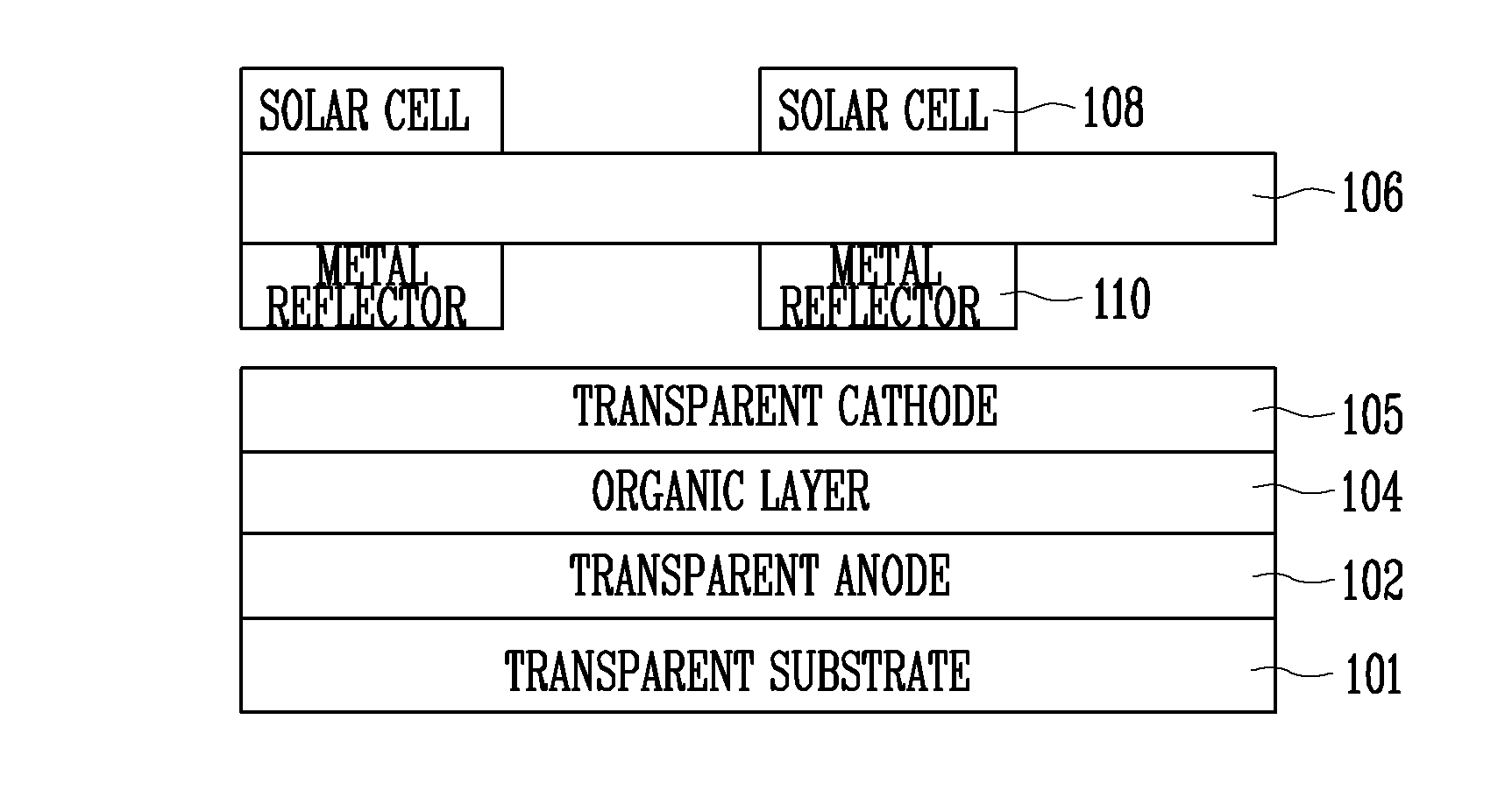
Transparent Organic Light Emitting Diode Lighting Device
PatentInactiveUS20100237374A1
Innovation
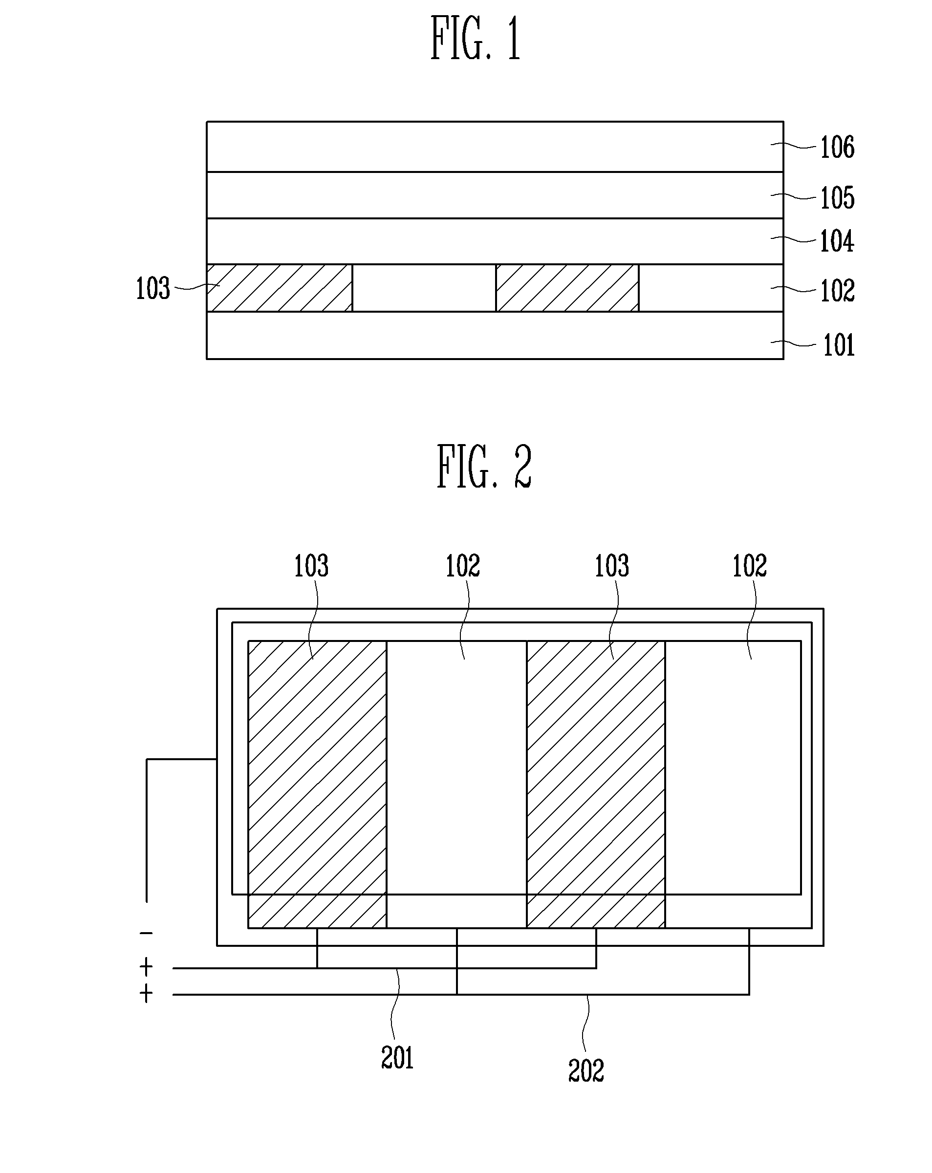
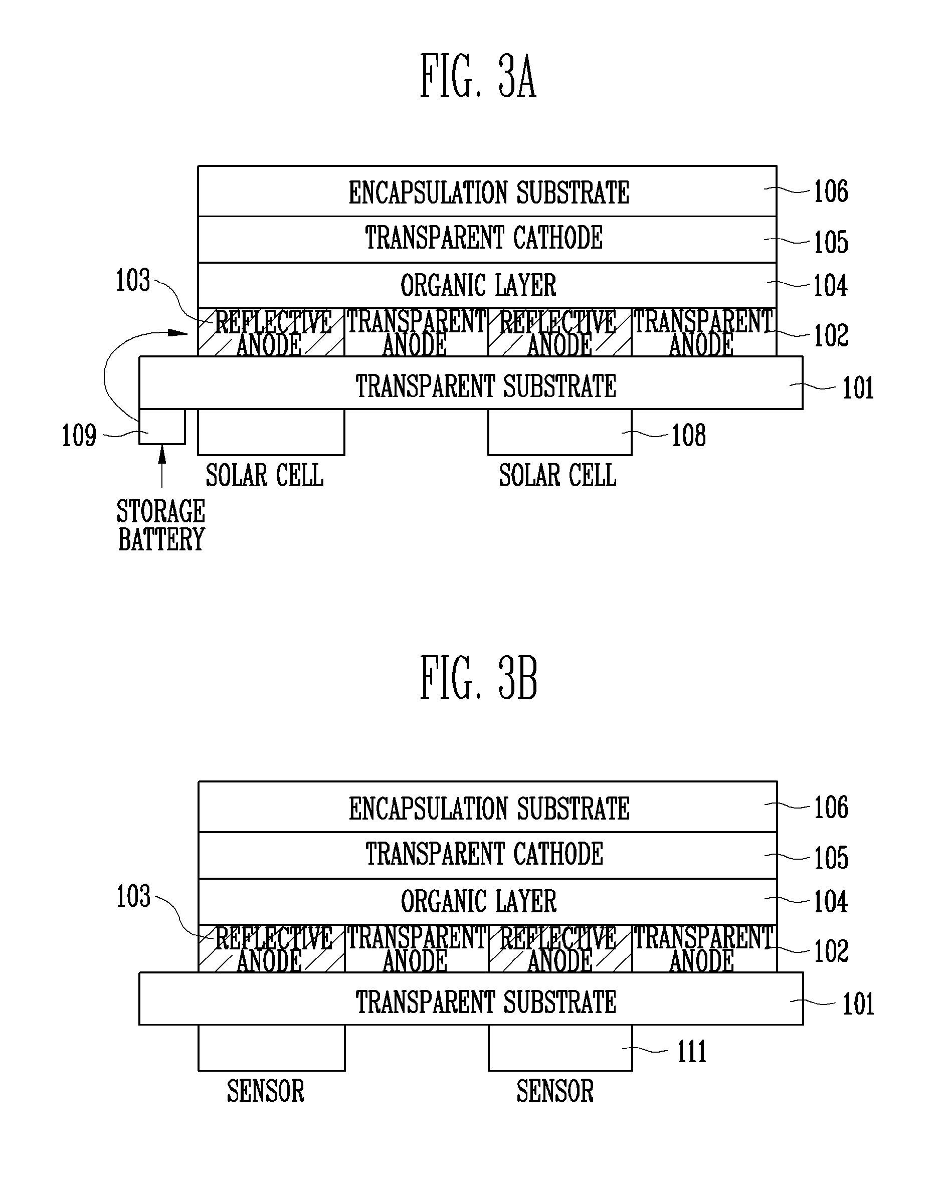
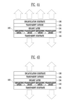
- A transparent OLED lighting device is designed with a transparent substrate, alternating transparent and reflective anodes, an organic layer, and a transparent cathode, where the light emission direction is controlled by current application to the anodes, and a metal reflector is used to direct light emission.
Environmental Impact of TCF Manufacturing
The manufacturing of transparent conductive films (TCFs) for OLED displays presents significant environmental challenges that warrant careful consideration as production scales increase to meet growing demand. Traditional TCF production processes, particularly those involving indium tin oxide (ITO), consume substantial energy during vacuum deposition and high-temperature annealing stages, contributing to considerable carbon emissions. A single manufacturing facility producing ITO films can consume electricity equivalent to thousands of households annually.
Material extraction represents another critical environmental concern. Indium, the primary component in ITO films, is classified as a critical raw material due to its scarcity and geographically concentrated mining operations. Current extraction methods generate substantial tailings and wastewater containing heavy metals that can contaminate local ecosystems when improperly managed. Studies indicate that for every kilogram of indium produced, approximately 600 kilograms of mining waste is generated.
Chemical processes in TCF manufacturing introduce additional environmental hazards. Etching procedures typically employ strong acids and solvents that require careful handling and disposal. These chemicals, including hydrofluoric acid and various chlorinated compounds, pose risks to aquatic ecosystems if released untreated into water systems. Industry data suggests that chemical waste from TCF production facilities can contain concentrations of hazardous substances exceeding environmental safety thresholds by factors of 10-100.
The end-of-life management of TCF-containing displays presents further environmental challenges. The complex integration of TCFs with other display components complicates recycling efforts, resulting in valuable materials being landfilled rather than recovered. Current estimates indicate less than 30% of indium from discarded displays is successfully reclaimed through existing recycling infrastructure.
Emerging alternative TCF technologies offer promising environmental improvements. Metal nanowire networks and carbon-based materials like graphene require less energy-intensive manufacturing processes and utilize more abundant raw materials. Life cycle assessments indicate that silver nanowire TCFs can reduce manufacturing energy requirements by up to 50% compared to traditional ITO, with corresponding reductions in greenhouse gas emissions.
Industry initiatives are increasingly focusing on developing closed-loop manufacturing systems for TCFs, with several major display manufacturers implementing water recycling programs that reduce freshwater consumption by 30-40%. Advanced filtration systems are being deployed to capture and reuse valuable materials from production waste streams, gradually moving the industry toward more sustainable practices as next-generation OLED displays enter mass production.
Supply Chain Resilience for TCF Materials
The resilience of transparent conductive film (TCF) supply chains has become a critical concern for the OLED display industry, particularly as these materials form the backbone of next-generation display technologies. Recent global disruptions, including the COVID-19 pandemic and geopolitical tensions, have exposed vulnerabilities in the TCF material supply network that threaten production continuity for display manufacturers.
The TCF supply chain is characterized by geographic concentration, with over 70% of indium tin oxide (ITO) production—the dominant TCF material—concentrated in East Asia. This regional dependency creates significant risk exposure, as evidenced by the 43% price volatility of indium observed between 2020-2022. Display manufacturers have begun implementing multi-sourcing strategies, with leading companies now maintaining relationships with at least three TCF suppliers across different regions.
Material diversification represents another key resilience strategy. The industry is actively qualifying alternative TCF materials such as silver nanowires, PEDOT:PSS, and graphene-based films to reduce dependency on ITO. These alternatives not only mitigate supply risks but also offer technical advantages for flexible OLED applications. Companies investing in material diversification have reported 30% lower supply disruption impacts during recent shortages.
Vertical integration efforts are accelerating among major display manufacturers, with several companies acquiring or establishing joint ventures with TCF material producers. This approach provides greater control over critical material inputs and has demonstrated a 25% reduction in lead time variability. Samsung Display and LG Display have notably invested in captive TCF production capabilities to ensure consistent quality and supply security.
Inventory management practices are evolving toward more sophisticated models that balance just-in-time efficiency with strategic stockpiling of critical TCF materials. Advanced analytics and AI-driven demand forecasting have enabled a 40% improvement in inventory optimization while maintaining supply assurance. The industry standard has shifted from 30-day to 60-90 day safety stocks for critical TCF components.
Technological innovation in manufacturing processes is also enhancing supply chain resilience. Developments in roll-to-roll processing and additive manufacturing techniques have reduced material waste by up to 35% and enabled more distributed production models. These advancements allow for smaller, more numerous production facilities closer to end markets, reducing logistics vulnerabilities and transportation-related carbon emissions by approximately 28%.
Unlock deeper insights with Patsnap Eureka Quick Research — get a full tech report to explore trends and direct your research. Try now!
Generate Your Research Report Instantly with AI Agent
Supercharge your innovation with Patsnap Eureka AI Agent Platform!