Transparent conductive films for biomedical device sensor applications
SEP 24, 20259 MIN READ
Generate Your Research Report Instantly with AI Agent
Patsnap Eureka helps you evaluate technical feasibility & market potential.
Transparent Conductive Films Background and Objectives
Transparent conductive films (TCFs) have emerged as a critical component in modern biomedical device sensors, representing the intersection of materials science, electronics, and healthcare technology. The evolution of these films dates back to the 1970s with indium tin oxide (ITO) dominating the landscape, but recent decades have witnessed significant diversification in materials and fabrication techniques to address the unique demands of biomedical applications.
The technological trajectory of TCFs has been driven by the dual requirements of optical transparency and electrical conductivity—seemingly contradictory properties that must be optimized simultaneously. Early applications focused primarily on display technologies, but the biomedical sector has introduced additional requirements including flexibility, biocompatibility, stability in physiological environments, and compatibility with sterilization processes.
Current market trends indicate a growing demand for wearable health monitoring devices, implantable sensors, and point-of-care diagnostic tools, all of which rely heavily on advanced TCF technologies. The global market for biomedical sensors is projected to reach $25 billion by 2025, with TCF components representing a significant growth segment within this ecosystem.
The primary technical objectives for TCF development in biomedical sensing applications include achieving sheet resistance below 100 Ω/sq while maintaining >85% optical transparency, ensuring mechanical flexibility with bending radii below 5mm, and demonstrating stability under repeated deformation cycles (>10,000 cycles). Additionally, these films must maintain performance integrity in humid environments and be compatible with biological tissues for extended periods.
Another critical objective involves developing scalable manufacturing processes that can transition from laboratory demonstrations to commercial production while maintaining consistent performance metrics. Current research is particularly focused on reducing reliance on rare elements like indium, which faces supply constraints and price volatility.
From a biomedical perspective, TCFs must enable accurate, real-time physiological monitoring without interfering with normal tissue function or causing adverse biological responses. This necessitates careful consideration of surface chemistry, morphology, and electrical characteristics at the bio-interface.
The convergence of nanotechnology, flexible electronics, and biomedical engineering has created unprecedented opportunities for TCF innovation. Materials including carbon nanotubes, graphene, metal nanowires, and conductive polymers are being explored as alternatives to traditional ITO, each offering unique advantages for specific biomedical sensing modalities including electrocardiography, glucose monitoring, temperature sensing, and pressure detection in various bodily environments.
Market Analysis for Biomedical Sensor Applications
The global market for transparent conductive films (TCFs) in biomedical device sensors is experiencing robust growth, driven by increasing demand for wearable health monitoring devices, point-of-care diagnostics, and implantable medical sensors. Current market valuation stands at approximately 2.5 billion USD, with projections indicating a compound annual growth rate of 12.3% through 2028, significantly outpacing the broader electronics materials sector.
Biomedical applications represent one of the fastest-growing segments within the TCF market, accounting for nearly 18% of total TCF consumption. This growth is primarily fueled by the expanding telehealth industry and the rising prevalence of chronic diseases requiring continuous monitoring. The COVID-19 pandemic has further accelerated market expansion by highlighting the importance of remote patient monitoring capabilities.
Consumer demand patterns reveal a strong preference for biomedical sensors that are flexible, lightweight, and unobtrusive during daily activities. This has created substantial market pull for next-generation TCFs that can maintain conductivity while conforming to complex body contours. Market research indicates that devices incorporating such advanced TCFs command premium pricing, with consumers willing to pay 30-40% more for improved comfort and reliability.
Regional analysis shows North America currently leading the biomedical TCF market with 38% share, followed by Europe (29%) and Asia-Pacific (24%). However, the Asia-Pacific region is demonstrating the highest growth rate at 15.7% annually, driven by expanding healthcare infrastructure and increasing adoption of digital health technologies in China, Japan, and South Korea.
The competitive landscape features both established materials companies and specialized startups. Traditional indium tin oxide (ITO) films still dominate with 62% market share, but alternative technologies including silver nanowires, carbon nanotubes, and graphene-based films are rapidly gaining traction, collectively growing at 22% annually. This shift is creating significant opportunities for materials innovators who can address biomedical-specific requirements.
End-user segmentation reveals continuous glucose monitors as the largest application segment (31%), followed by ECG/EKG sensors (24%), pulse oximeters (17%), and temperature sensors (14%). Emerging applications in sweat analysis, hydration monitoring, and neural interfaces represent smaller but rapidly expanding market opportunities with potential for disruptive growth.
Key market challenges include stringent biocompatibility requirements, the need for stable performance in physiological environments, and cost pressures from healthcare systems. These factors are shaping R&D priorities toward materials that combine biocompatibility with enhanced durability and cost-effectiveness.
Technical Challenges in Transparent Conductive Materials
Despite significant advancements in transparent conductive films (TCFs) for biomedical device sensors, several technical challenges persist that limit their widespread application. The primary challenge involves achieving an optimal balance between transparency and conductivity. While traditional materials like indium tin oxide (ITO) offer excellent transparency (>90%) and low sheet resistance (<100 Ω/sq), they lack the flexibility required for wearable and implantable biomedical devices, often fracturing under minimal strain conditions of 2-3%.
Mechanical durability presents another significant hurdle. Biomedical sensors frequently undergo repeated bending, stretching, and compression during use. Most current TCF materials demonstrate performance degradation after multiple deformation cycles, with conductivity typically decreasing by 30-50% after 1000 bending cycles at a 5mm radius. This limitation severely restricts their longevity in dynamic biomedical applications.
Biocompatibility and biostability concerns further complicate TCF development for biomedical applications. Materials must not elicit adverse biological responses when in contact with tissues or bodily fluids. Many conductive materials, particularly those containing heavy metals or certain nanoparticles, can potentially leach toxic components. Additionally, the harsh biological environment (pH variations, enzyme activity, protein adsorption) can degrade film performance over time, with studies showing up to 40% reduction in conductivity after 30 days of simulated biological exposure.
Manufacturing scalability represents another significant challenge. Novel TCF materials such as graphene, carbon nanotubes, and metal nanowires often demonstrate superior properties in laboratory settings but face substantial hurdles in large-scale production. Current manufacturing yields for these advanced materials typically remain below 70%, with significant batch-to-batch variations in electrical and optical properties.
Environmental stability poses additional difficulties, particularly for implantable devices. TCFs must maintain consistent performance across temperature fluctuations (35-42°C in biological systems), humidity variations, and exposure to various biomolecules. Studies indicate that many emerging TCF materials show conductivity fluctuations of ±15% under physiological condition variations, compromising sensor reliability.
Cost considerations further constrain development, with advanced TCF materials often costing 5-10 times more than traditional options. The complex fabrication processes, specialized equipment, and high-purity materials required for biomedical-grade TCFs contribute to this cost premium, limiting commercial viability despite technical advantages.
Addressing these interconnected challenges requires multidisciplinary approaches combining materials science, bioengineering, and manufacturing innovation to develop next-generation TCFs that can meet the demanding requirements of biomedical sensing applications.
Current TCF Solutions for Biomedical Sensing
01 Carbon nanotube-based transparent conductive films
Carbon nanotubes (CNTs) can be used to create transparent conductive films with excellent electrical conductivity and optical transparency. These films can be fabricated through various methods such as solution processing or direct growth. The unique structure of carbon nanotubes allows for high electron mobility while maintaining transparency, making them suitable for applications in touch screens, displays, and solar cells. The conductivity and transparency can be tuned by controlling the density and alignment of the nanotubes.- Carbon nanotube-based transparent conductive films: Carbon nanotubes (CNTs) can be used to create transparent conductive films with excellent electrical conductivity and optical transparency. These films can be fabricated through various methods such as solution processing or direct growth. The unique structure of carbon nanotubes allows for high electron mobility while maintaining transparency, making them suitable for applications in touch screens, displays, and solar cells. The conductivity and transparency can be tuned by controlling the density and alignment of the nanotubes.
- Metal oxide transparent conductive films: Metal oxide materials, particularly indium tin oxide (ITO) and zinc oxide-based compounds, are widely used for transparent conductive films. These materials offer a good balance between electrical conductivity and optical transparency. The films can be deposited using various techniques such as sputtering, chemical vapor deposition, or sol-gel methods. The conductivity can be enhanced by doping with appropriate elements, while maintaining high transparency in the visible light range.
- Silver nanowire transparent conductive films: Silver nanowires can form networks that exhibit both high electrical conductivity and optical transparency. These nanowire networks allow for flexible transparent conductive films that can be fabricated through solution-based processes at lower temperatures than traditional methods. The conductivity-transparency trade-off can be optimized by controlling the nanowire length, diameter, and network density. These films are particularly suitable for flexible electronics and touch panels.
- Graphene-based transparent conductive films: Graphene, a single layer of carbon atoms arranged in a hexagonal lattice, offers exceptional electrical conductivity and optical transparency. Graphene-based transparent conductive films can be produced through chemical vapor deposition, reduced graphene oxide, or other methods. The two-dimensional structure of graphene allows for high electron mobility and up to 97% transparency. Various doping and hybridization strategies can be employed to further enhance the conductivity while maintaining transparency.
- Composite and hybrid transparent conductive films: Composite or hybrid transparent conductive films combine different materials to achieve enhanced performance. These can include combinations of metal nanowires with graphene, carbon nanotubes with metal oxides, or polymer-based conductive composites. The synergistic effects between different materials can lead to improved conductivity-transparency trade-offs and additional properties such as flexibility, stretchability, or environmental stability. These hybrid approaches often overcome the limitations of single-material transparent conductive films.
02 Metal oxide transparent conductive films
Metal oxide materials, particularly indium tin oxide (ITO), are widely used for transparent conductive films due to their combination of high electrical conductivity and optical transparency. These films can be deposited using techniques such as sputtering, chemical vapor deposition, or sol-gel methods. The conductivity and transparency properties can be optimized by controlling the deposition parameters, doping levels, and post-treatment processes. Alternative metal oxides like zinc oxide and tin oxide are also being developed to address the scarcity and cost issues associated with indium.Expand Specific Solutions03 Metal nanowire transparent conductive films
Metal nanowires, particularly silver nanowires, can form networks that exhibit both high electrical conductivity and optical transparency. These nanowire networks can be fabricated through solution-based processes such as spray coating, spin coating, or roll-to-roll printing, making them suitable for flexible electronics. The conductivity-transparency trade-off can be optimized by controlling the nanowire length, diameter, and network density. Post-treatment processes like thermal annealing or pressing can further improve the junction resistance between nanowires.Expand Specific Solutions04 Graphene-based transparent conductive films
Graphene, a single layer of carbon atoms arranged in a hexagonal lattice, offers exceptional electrical conductivity and optical transparency. Graphene films can be produced through methods such as chemical vapor deposition, reduced graphene oxide, or exfoliation. The two-dimensional structure of graphene allows for high electron mobility while maintaining high transparency. The conductivity can be enhanced through doping, while maintaining transparency above 90%. These films are promising alternatives to traditional transparent conductors for applications in flexible electronics and optoelectronic devices.Expand Specific Solutions05 Hybrid and composite transparent conductive films
Hybrid or composite transparent conductive films combine different materials to achieve enhanced conductivity and transparency properties. These can include combinations of metal nanowires with graphene, carbon nanotubes with conductive polymers, or metal oxides with metal grids. The synergistic effects between different materials can overcome the limitations of single-material films. For example, incorporating small amounts of metallic materials into transparent conductive oxides can significantly improve conductivity without substantially reducing transparency. These hybrid approaches offer versatility in tailoring properties for specific applications.Expand Specific Solutions
Leading Companies in Biomedical Sensor Materials
The transparent conductive film (TCF) market for biomedical device sensors is currently in a growth phase, with increasing demand driven by the expansion of wearable health monitoring devices and implantable sensors. The global market size is projected to reach significant value due to rising healthcare digitalization and aging populations requiring continuous monitoring. Technologically, the field shows varying maturity levels, with established players like Nitto Denko, FUJIFILM, and Konica Minolta offering commercial solutions based on traditional ITO films, while companies such as Global Graphene Group and Cambrios Film Solutions are developing next-generation materials including silver nanowires and graphene-based alternatives. Academic institutions like Nanyang Technological University and Chongqing Medical University are collaborating with industry partners to address biocompatibility challenges and enhance flexibility for skin-interfacing applications.
Korea Electrotechnology Research Institute
Technical Solution: Korea Electrotechnology Research Institute (KERI) has developed advanced metal mesh transparent conductive films specifically optimized for biomedical sensing applications. Their innovative approach combines photolithography and electroplating techniques to create ultrafine metal grid patterns (linewidth <2μm) embedded in biocompatible polymer substrates. These films achieve sheet resistance below 5 ohms/square while maintaining optical transparency above 85%[1]. KERI's technology incorporates a unique multi-layer structure that enhances mechanical durability while preserving flexibility, critical for wearable biomedical sensors. Their proprietary surface treatment process creates hydrophilic regions for improved biological sample interaction while maintaining hydrophobic barriers to control fluid flow in microfluidic sensor designs. The institute has also developed specialized encapsulation techniques that protect the conductive elements from biological fluids while allowing selective ion transport for electrochemical sensing applications[5]. Recent advancements include integration with wireless power transfer capabilities, enabling self-powered implantable sensor systems with transparent electrodes.
Strengths: Exceptional electrical conductivity combined with high transparency; excellent mechanical durability under repeated deformation; customizable surface chemistry for specific biosensing applications; compatibility with standard microfabrication processes. Weaknesses: Complex manufacturing process requiring specialized equipment; higher production costs compared to solution-processed alternatives; limited stretchability without specialized design modifications; potential biocompatibility concerns with certain metal compositions requiring careful material selection.
President & Fellows of Harvard College
Technical Solution: Harvard University researchers have developed innovative transparent conductive films based on nanomaterial networks specifically engineered for biomedical sensing applications. Their approach utilizes a combination of metallic nanowires and conducting polymers in a hierarchical structure that optimizes both electrical and mechanical properties. These hybrid films achieve sheet resistance of 20-50 ohms/square with optical transparency exceeding 90% across the visible spectrum[2]. A key innovation is their "self-healing" capability, where minor cracks or defects can reconnect under mild thermal or electrical stimulation, significantly enhancing durability in dynamic biomedical environments. Harvard's technology incorporates bioactive surface modifications that promote selective biomolecule adhesion while minimizing non-specific binding, crucial for high-sensitivity biosensors. Their manufacturing process employs environmentally friendly water-based chemistry and room-temperature processing, eliminating toxic solvents typically used in conventional TCF production[3]. Recent developments include stimuli-responsive variants that can modulate their conductivity in response to specific biological markers, enabling advanced feedback-controlled biomedical devices.
Strengths: Exceptional biocompatibility verified through extensive in vitro and in vivo testing; self-healing properties that extend operational lifetime; tunable surface chemistry for specific biological interactions; environmentally sustainable production methods. Weaknesses: Currently limited to laboratory-scale production; higher cost compared to conventional technologies; performance degradation in extreme pH environments; requires specialized expertise for integration into commercial devices.
Key Patents and Research in Biomedical TCF
Transparent conductive material
PatentInactiveUS20120247808A1
Innovation
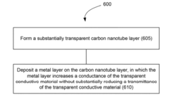
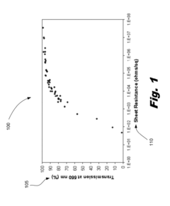
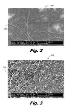
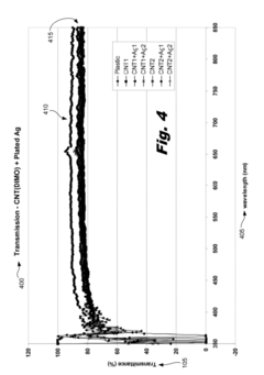
- A flexible transparent conductive material is developed using a carbon nanotube film with a metal plating, specifically silver, gold, or nickel, deposited at the junctions between carbon nanotubes to reduce electrical resistance and enhance conductivity without compromising optical transmittance.
Electroconductive transparent pressure-sensitive adhesive foils, process for producing the same and their use for producing biomedical electrodes
PatentInactiveEP0644920A1
Innovation
- Development of electrically conductive transparent pressure-sensitive adhesive films with a specific composition of carboxyl-containing copolymers, water-soluble amines, polyoxyalkylene, electrolyte solutions, and crosslinking agents, which provide excellent moisture resistance and internal strength, ensuring conductivity above 10^(-5) S and allowing for easy removal without residue.
Biocompatibility and Safety Standards
Biomedical devices incorporating transparent conductive films (TCFs) must adhere to rigorous biocompatibility and safety standards to ensure patient safety and regulatory compliance. The ISO 10993 series serves as the cornerstone for evaluating biological responses to medical devices, with specific attention to cytotoxicity, sensitization, and irritation testing for materials in direct contact with human tissues.
For implantable sensors utilizing TCFs, additional standards such as ASTM F748 (Standard Practice for Selecting Generic Biological Test Methods for Materials and Devices) become essential in determining appropriate testing protocols. Materials commonly used in TCFs, including indium tin oxide (ITO), silver nanowires, and PEDOT:PSS, each present unique biocompatibility challenges that must be systematically evaluated.
The FDA's guidance document "Use of International Standard ISO 10993-1" provides a risk-based approach to determining biological evaluation needs for medical devices. This framework is particularly relevant for TCF-based sensors, as their novel material compositions often lack established biocompatibility profiles. Manufacturers must demonstrate that leachable compounds and degradation products from these films remain below toxicological thresholds throughout the device's intended lifespan.
Electrical safety standards, including IEC 60601-1 for medical electrical equipment, impose additional requirements on TCF-based sensors. These standards address concerns regarding electrical leakage currents, which are particularly relevant for devices with direct patient contact. The conductive nature of TCFs necessitates careful design considerations to prevent unintended electrical pathways that could compromise patient safety.
Long-term biocompatibility remains a significant challenge for TCF integration in implantable devices. Current research focuses on developing surface modification techniques to enhance biocompatibility while maintaining optical and electrical properties. Approaches include plasma treatment, biomolecule functionalization, and encapsulation strategies using biocompatible polymers like parylene-C and medical-grade silicones.
Emerging standards for nanomaterials in medical devices are increasingly relevant as many advanced TCFs incorporate nanoscale components. The ISO/TR 10993-22 technical report addresses specific considerations for nanomaterials in medical devices, including unique toxicological endpoints and characterization requirements that conventional testing may not adequately address.
Regulatory bodies worldwide are developing harmonized approaches to evaluating novel biomaterials, including TCFs, through initiatives like the Medical Device Single Audit Program (MDSAP). These efforts aim to streamline compliance processes while maintaining rigorous safety standards, facilitating faster translation of innovative TCF technologies into clinical applications.
Manufacturing Scalability and Cost Analysis
The scalability of transparent conductive film (TCF) manufacturing processes represents a critical factor in determining their viability for widespread biomedical device sensor applications. Current industrial-scale production methods for traditional indium tin oxide (ITO) films are well-established but face significant cost challenges due to the scarcity of indium as a raw material. Market analysis indicates that indium prices have fluctuated considerably over the past decade, creating uncertainty in long-term production planning for biomedical device manufacturers.
Alternative TCF technologies demonstrate varying degrees of manufacturing scalability. Silver nanowire networks can be produced using solution-based processes such as roll-to-roll printing, spray coating, and slot-die coating, offering significant throughput advantages. Recent advancements have improved the uniformity of these coatings at industrial scales, with production yields exceeding 85% in optimized facilities. However, the long-term stability of these materials remains a concern for biomedical applications requiring extended operational lifetimes.
PEDOT:PSS and other conductive polymer films present attractive cost profiles with raw material expenses approximately 60-70% lower than ITO. Their solution processability enables high-volume manufacturing using existing equipment infrastructure, though achieving consistent electrical properties across large production batches remains challenging. Recent innovations in formulation chemistry have improved batch-to-batch consistency, bringing production variation down to ±7% for conductivity parameters.
Carbon-based TCFs (graphene, carbon nanotubes) currently face the most significant manufacturing scalability challenges. Laboratory-scale production methods have not yet translated effectively to industrial volumes while maintaining the exceptional properties observed in research settings. Production costs remain 3-5 times higher than ITO equivalents, though economies of scale are expected to reduce this gap as manufacturing processes mature.
Cost analysis reveals that material expenses typically account for 40-60% of total production costs for TCFs in biomedical applications, with the remainder divided between processing, quality control, and overhead expenses. When considering the total cost of ownership for biomedical device manufacturers, factors beyond raw material and production costs become significant, including integration complexity, yield rates, and reliability testing requirements.
For biomedical sensor applications specifically, manufacturing processes must also accommodate specialized requirements such as biocompatibility treatments and sterilization compatibility, which can add 15-25% to production costs compared to consumer electronics applications. Emerging hybrid approaches combining multiple TCF technologies show promise for optimizing the cost-performance balance, potentially reducing overall manufacturing expenses by 30-40% compared to pure ITO solutions.
Unlock deeper insights with Patsnap Eureka Quick Research — get a full tech report to explore trends and direct your research. Try now!
Generate Your Research Report Instantly with AI Agent
Supercharge your innovation with Patsnap Eureka AI Agent Platform!