Transparent conductive films market regulations and qualification requirements
SEP 24, 20259 MIN READ
Generate Your Research Report Instantly with AI Agent
Patsnap Eureka helps you evaluate technical feasibility & market potential.
TCF Technology Background and Objectives
Transparent conductive films (TCFs) have evolved significantly since their inception in the early 20th century, with indium tin oxide (ITO) emerging as the dominant material since the 1970s. These films serve as critical components in modern electronic devices, providing the essential combination of optical transparency and electrical conductivity required for touchscreens, displays, photovoltaic cells, and various smart devices. The global TCF market has experienced exponential growth alongside the expansion of consumer electronics and renewable energy sectors.
The technological evolution of TCFs has been driven by several factors, including the increasing demand for flexible electronics, the scarcity of indium resources, and the push for more sustainable manufacturing processes. Initially developed for military applications and specialized industrial uses, TCFs have now become ubiquitous in consumer products, necessitating standardized regulations and qualification requirements across international markets.
Current technological objectives in the TCF sector focus on addressing several key challenges. First, developing alternative materials to ITO that offer comparable performance while reducing dependency on scarce indium resources. Second, enhancing flexibility and durability to meet the growing demand for bendable and foldable display technologies. Third, improving manufacturing scalability and cost-effectiveness to support mass production requirements. Fourth, meeting increasingly stringent environmental regulations regarding production processes and material recyclability.
The regulatory landscape for TCFs has become increasingly complex as these materials find applications in diverse industries with varying safety, performance, and environmental standards. Different regions have established specific qualification requirements that manufacturers must meet to access markets, creating a fragmented regulatory environment that presents significant challenges for global supply chains.
Technical objectives for the industry include standardizing testing methodologies for optical transparency, electrical conductivity, mechanical flexibility, and environmental durability. Additionally, there is a growing focus on developing universal certification frameworks that can harmonize requirements across different regions and applications, reducing compliance costs and market entry barriers for manufacturers.
As emerging technologies like Internet of Things (IoT) devices, augmented reality, and transparent electronics gain traction, the TCF industry faces new regulatory challenges related to product longevity, electromagnetic interference, and integration with other electronic components. The technical community aims to establish forward-looking standards that can accommodate these evolving applications while ensuring consumer safety and product reliability.
Market Demand Analysis for Transparent Conductive Films
The transparent conductive films (TCF) market is experiencing robust growth driven by the expanding electronics industry, particularly in touch screens, displays, photovoltaics, and emerging flexible electronics. Current market analysis indicates that the global TCF market is projected to grow at a compound annual growth rate of 8.5% through 2028, with the Asia-Pacific region maintaining its dominant position as both the largest producer and consumer.
Consumer electronics remains the primary demand driver, accounting for approximately 65% of TCF consumption. Smartphone and tablet manufacturers continue to seek higher performance films with improved optical clarity, lower resistance, and enhanced durability. The average replacement cycle for smartphones has shortened to 24 months in developed markets, sustaining steady demand for TCF components.
Automotive applications represent the fastest-growing segment, with advanced driver-assistance systems (ADAS) and in-vehicle infotainment systems incorporating more touch interfaces. This sector demands TCFs with exceptional environmental stability and reliability under extreme temperature conditions, creating premium pricing opportunities for specialized products.
The renewable energy sector, particularly photovoltaics, constitutes another significant market for TCFs. Solar panel manufacturers require films with high transparency and conductivity to maximize energy conversion efficiency. As global solar installation capacity continues to expand at double-digit rates annually, this application presents substantial growth potential for TCF suppliers.
Emerging applications in smart wearables, flexible displays, and Internet of Things (IoT) devices are creating new demand vectors. These applications often require TCFs with specialized properties such as flexibility, stretchability, and compatibility with non-traditional substrates. Market research indicates that flexible electronics applications will grow at twice the rate of traditional applications over the next five years.
Regional demand patterns show significant variation, with North American and European markets prioritizing performance and reliability, while price sensitivity remains higher in developing markets. However, this gap is narrowing as quality expectations rise globally. The premium segment focusing on high-performance TCFs for specialized applications shows stronger profit margins compared to the mass-market segment.
Customer requirements are evolving toward thinner, more durable films with improved optical and electrical properties. Manufacturers report increasing pressure to deliver TCFs with transmittance above 90% while maintaining sheet resistance below 100 ohms/square. Additionally, environmental considerations are gaining importance, with customers increasingly requesting halogen-free and recyclable materials to meet sustainability objectives and comply with evolving regulations.
Global TCF Technology Status and Challenges
Transparent conductive films (TCFs) have become a critical component in modern electronics, with global market adoption accelerating across multiple industries. Currently, indium tin oxide (ITO) dominates the commercial TCF landscape, accounting for approximately 85% of market share due to its excellent combination of optical transparency and electrical conductivity. However, ITO faces significant limitations including brittleness, limited flexibility, and the scarcity of indium resources, which have driven extensive research into alternative materials.
The global TCF technology landscape shows regional specialization patterns. East Asian countries, particularly South Korea, Japan, and Taiwan, lead in ITO film production and advanced manufacturing techniques. China has rapidly expanded its TCF manufacturing capacity, though often focusing on mid-range applications. North American and European entities generally concentrate on next-generation materials research, including carbon nanotubes, graphene, and metal nanowires.
A primary technical challenge facing the TCF industry is achieving the optimal balance between transparency and conductivity. Current alternatives to ITO, while promising in flexibility and cost, typically underperform in this critical trade-off. Silver nanowire networks offer excellent conductivity but struggle with long-term stability and uniformity in large-area applications. Carbon-based materials like graphene demonstrate theoretical superiority but face significant manufacturing scalability issues.
Regulatory frameworks present another substantial challenge, with inconsistent global standards creating market fragmentation. The European Union's RoHS and REACH regulations impose strict limitations on hazardous substances, affecting TCF manufacturing processes. Similarly, Japan's JIS standards and South Korea's KC certification create region-specific compliance requirements. The United States lacks a unified federal standard, instead relying on industry-specific requirements from bodies like ASTM International.
Environmental sustainability represents an emerging challenge, with increasing pressure to develop eco-friendly manufacturing processes and end-of-life recycling solutions. The indium recovery rate from discarded displays remains below 1%, creating significant resource inefficiency. Additionally, many alternative TCF technologies rely on toxic solvents or energy-intensive processes that face growing regulatory scrutiny.
Qualification testing requirements vary significantly across applications, with consumer electronics typically requiring 5,000-10,000 flex cycles for durability, while automotive applications demand up to 100,000 cycles plus temperature cycling from -40°C to 85°C. These divergent requirements complicate the development of universally applicable TCF solutions and necessitate application-specific optimization.
Current TCF Technical Solutions
01 Carbon nanotube-based transparent conductive films
Carbon nanotubes (CNTs) can be used to create highly transparent and conductive films. These films offer excellent electrical conductivity while maintaining high optical transparency, making them suitable for various electronic applications. The CNTs can be dispersed in solutions and coated onto substrates using methods such as spray coating or vacuum filtration. These films can be flexible and have adjustable conductivity based on the density and alignment of the nanotubes.- Carbon nanotube-based transparent conductive films: Carbon nanotubes (CNTs) can be used to create highly transparent and conductive films. These films offer excellent electrical conductivity while maintaining high optical transparency, making them suitable for various electronic applications. The CNTs can be dispersed in solutions and deposited onto substrates using methods such as spray coating or vacuum filtration. These films can be flexible and have adjustable conductivity based on the concentration and arrangement of the nanotubes.
- Metal oxide-based transparent conductive films: Metal oxides, particularly indium tin oxide (ITO), are widely used for transparent conductive films. These materials provide a good balance of optical transparency and electrical conductivity. The films can be deposited using techniques such as sputtering, chemical vapor deposition, or sol-gel processes. Metal oxide films are commonly used in displays, touch screens, and photovoltaic devices. Alternative metal oxides are being developed to replace ITO due to the scarcity and cost of indium.
- Silver nanowire transparent conductive films: Silver nanowires can be used to create networks that form transparent conductive films. These nanowires create conductive pathways while allowing light to pass through the spaces between them. The films can be fabricated through solution-based processes such as spray coating, spin coating, or roll-to-roll printing. Silver nanowire films offer advantages including high flexibility, stretchability, and compatibility with various substrates. They are particularly suitable for flexible electronics and touch screen applications.
- Graphene-based transparent conductive films: Graphene, a single layer of carbon atoms arranged in a hexagonal lattice, can be used to create highly transparent and conductive films. These films exhibit exceptional electrical conductivity, optical transparency, and mechanical flexibility. Graphene films can be produced through methods such as chemical vapor deposition, reduced graphene oxide, or exfoliation techniques. The properties of graphene films can be tuned by controlling the number of layers, doping, or creating hybrid structures with other materials.
- Hybrid and composite transparent conductive films: Hybrid or composite transparent conductive films combine multiple materials to achieve enhanced performance. These films may incorporate combinations of metal nanowires, carbon nanotubes, graphene, metal oxides, or conductive polymers. The hybrid approach allows for optimization of electrical, optical, and mechanical properties beyond what can be achieved with single-material films. These composite structures can overcome limitations of individual materials, such as improving stability, reducing sheet resistance, or enhancing flexibility.
02 Metal oxide-based transparent conductive films
Metal oxides, particularly indium tin oxide (ITO), are widely used for transparent conductive films. These materials provide a good balance of optical transparency and electrical conductivity. The films can be deposited using various techniques such as sputtering, chemical vapor deposition, or sol-gel methods. Metal oxide films are commonly used in displays, touch panels, and photovoltaic devices. Alternative metal oxides are being developed to replace ITO due to the scarcity and cost of indium.Expand Specific Solutions03 Silver nanowire transparent conductive films
Silver nanowires can be used to create transparent conductive films with excellent electrical and optical properties. These nanowires form a conductive network while allowing light to pass through the gaps between them. The films can be fabricated using solution-based processes such as spray coating, spin coating, or roll-to-roll printing. Silver nanowire films offer advantages such as flexibility, stretchability, and compatibility with various substrates, making them suitable for flexible electronics and touch screens.Expand Specific Solutions04 Graphene-based transparent conductive films
Graphene, a single layer of carbon atoms arranged in a hexagonal lattice, can be used to create transparent conductive films with exceptional properties. These films exhibit high electrical conductivity, optical transparency, and mechanical flexibility. Graphene films can be produced through methods such as chemical vapor deposition, reduced graphene oxide, or exfoliation. The unique combination of properties makes graphene films promising for applications in flexible electronics, solar cells, and touch screens.Expand Specific Solutions05 Hybrid and composite transparent conductive films
Hybrid or composite transparent conductive films combine different materials to achieve enhanced performance. These films may incorporate combinations of metal nanowires, carbon nanotubes, graphene, metal oxides, or conductive polymers. By combining materials with complementary properties, these hybrid films can achieve improved conductivity, transparency, flexibility, and stability. The synergistic effects between different components can overcome limitations of single-material films and enable new applications in optoelectronic devices.Expand Specific Solutions
Major TCF Industry Players Analysis
The transparent conductive films market is currently in a growth phase, driven by increasing demand in electronics, displays, and photovoltaic applications. The global market size is expanding rapidly, expected to reach significant valuation due to proliferation of touch-enabled devices and flexible electronics. Technologically, the field shows varying maturity levels with established players like AGC, Nitto Denko, and LG Chem offering commercial solutions, while companies such as Toray Advanced Film and JSR Corp focus on next-generation materials. Asian manufacturers, particularly from Japan, South Korea, and China (including Zhejiang Jingyi and Shanghai Langyi), dominate the landscape. Regulatory frameworks and qualification requirements are becoming more stringent, emphasizing environmental compliance, performance standardization, and reliability testing across global markets.
Nitto Denko Corp.
Technical Solution: Nitto Denko has developed ELECRYSTA™, a series of transparent conductive films that comply with global regulatory standards. Their TCFs meet Japan's Industrial Standards (JIS) C5010 for electrical properties and JIS K7105 for optical characteristics[1]. The company has obtained UL certification for their films, ensuring compliance with North American safety standards[2]. Nitto's manufacturing facilities maintain ISO 9001:2015 and ISO 14001:2015 certifications, guaranteeing consistent quality and environmental management[3]. Their TCFs undergo rigorous qualification testing including 1000-hour high temperature/high humidity exposure (85°C/85% RH) and 100,000 cycle bending tests according to IEC 62715-6-1 standards for mechanical durability[4]. Nitto's products comply with EU RoHS Directive 2011/65/EU and REACH Regulation EC 1907/2006, with full material declarations available to customers[5]. The company also meets the requirements of IEC 62788-1-5 for edge sealing materials used in photovoltaic modules.
Strengths: Excellent balance of optical clarity and conductivity; superior environmental stability in high humidity conditions; comprehensive global regulatory compliance. Weaknesses: Higher cost compared to conventional ITO films; limited flexibility in extreme cold environments; requires specialized handling during manufacturing integration.
AGC, Inc. (Japan)
Technical Solution: AGC has pioneered regulatory-compliant transparent conductive films through their EXCLEAR® product line, which utilizes a proprietary metal mesh technology. Their TCFs comply with Japan's Industrial Safety and Health Act and have received UL certification for safety standards in North America[1]. AGC's films meet the stringent requirements of IEC 61215 for long-term reliability and IEC 61646 for environmental testing[2]. The company has implemented a comprehensive qualification process that includes 1000-hour damp heat testing at 85°C/85% RH and adhesion testing according to ASTM D3359 standards[3]. Their TCFs have achieved ISO 10993 biocompatibility certification for wearable device applications and comply with EU's RoHS and REACH regulations[4]. AGC's manufacturing facilities maintain ISO 9001 and ISO 14001 certifications, ensuring consistent quality and environmental management systems throughout production[5].
Strengths: Exceptional durability with proven performance in extreme environmental conditions; comprehensive global regulatory compliance; versatile application range from consumer electronics to automotive displays. Weaknesses: Higher cost structure compared to emerging alternatives; limited scalability for very large area applications; requires specialized bonding techniques for optimal integration.
Key TCF Patents and Technical Literature
Method of manufacturing transparent conductive film, the transparent conductive film, element and transparent conductive substrate using the film, as well as device using the substrate
PatentInactiveUS9701849B2
Innovation
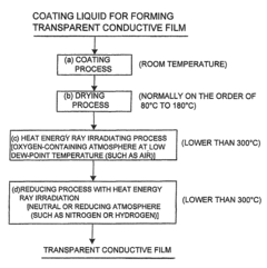
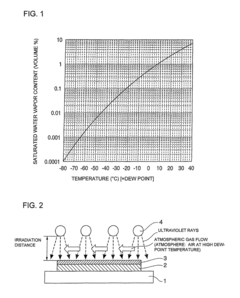
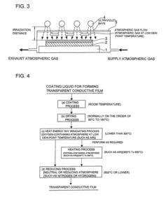
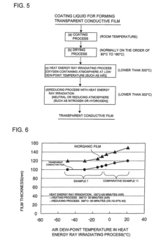
- A method involving a coating process with a liquid containing organic indium, tin, or zinc compounds, followed by energy ray irradiation under an oxygen-containing atmosphere at a low dew-point temperature, which promotes mineralization and densification of the film, forming a densely packed conductive oxide fine-particle layer with improved transparency, conductivity, and strength.
Transparent conductive films
PatentInactiveJP2013127985A
Innovation
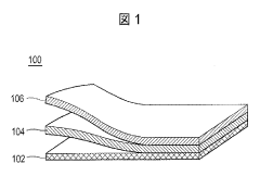
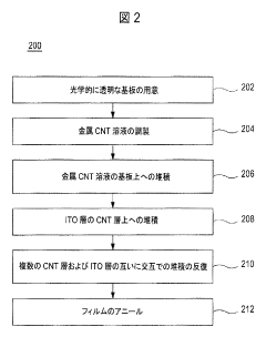
- A composite film comprising a carbon nanotube network and indium tin oxide layers, formed through methods like laser ablation, chemical vapor deposition, and sputtering, enhances conductivity and flexibility.
Regulatory Framework and Compliance Requirements
The regulatory landscape for transparent conductive films (TCFs) is complex and varies significantly across regions, creating a multifaceted compliance environment for manufacturers and suppliers. In the United States, TCFs must adhere to standards set by the Federal Communications Commission (FCC) for electromagnetic compatibility when used in electronic devices. Additionally, the Environmental Protection Agency (EPA) regulates the use of certain materials in TCFs, particularly those containing rare earth elements or potentially hazardous substances.
The European Union implements more stringent regulations through the Restriction of Hazardous Substances (RoHS) Directive, which limits the use of specific hazardous materials in electrical and electronic products. TCFs containing indium tin oxide (ITO) must comply with these restrictions, especially regarding heavy metal content. The EU's Registration, Evaluation, Authorization and Restriction of Chemicals (REACH) regulation further requires manufacturers to register chemical substances used in TCF production and provide safety data.
In Asia, Japan's Ministry of Economy, Trade and Industry (METI) has established the J-Moss (Japanese Material Declaration) standard, which requires disclosure of specific chemical substances in electronic products. China has implemented the China RoHS (Administrative Measure on the Control of Pollution Caused by Electronic Information Products), which mandates similar restrictions on hazardous substances in electronic products, including those utilizing TCFs.
Quality certification requirements for TCFs typically include ISO 9001 for quality management systems and ISO 14001 for environmental management systems. Specific to TCFs, the International Electrotechnical Commission (IEC) has developed standards for optical and electrical properties, including IEC 61646 for thin-film photovoltaic modules, which may apply to certain TCF applications in solar technology.
Performance qualification standards focus on key parameters such as optical transparency (typically requiring >80% in the visible spectrum), sheet resistance (commonly <100 ohms/square), and environmental stability. ASTM International provides testing methods for these properties, including ASTM D1003 for transparency and haze measurements and ASTM F390 for sheet resistance testing.
Emerging regulations are increasingly focusing on sustainability aspects of TCFs. The EU's Circular Economy Action Plan and similar initiatives worldwide are pushing for improved recyclability and reduced environmental impact of electronic components, including TCFs. This trend is driving research toward more environmentally friendly alternatives to traditional ITO-based films, such as silver nanowire, graphene, and conductive polymer technologies.
Environmental Impact and Sustainability Considerations
The environmental impact of transparent conductive films (TCFs) has become a critical consideration in market regulations and qualification requirements globally. Manufacturing processes for traditional indium tin oxide (ITO) films involve energy-intensive sputtering techniques and rare earth metals, raising significant sustainability concerns. Recent regulatory frameworks in the EU, North America, and Asia have established increasingly stringent environmental standards for TCF production, focusing on reducing carbon footprints and minimizing hazardous waste generation.
Life cycle assessments of TCFs reveal that indium extraction and processing contribute substantially to environmental degradation, with estimates suggesting that ITO-based technologies generate 30-40% more greenhouse gas emissions compared to emerging alternatives. This has prompted regulatory bodies to implement mandatory environmental impact reporting for manufacturers, with particular emphasis on resource depletion metrics and end-of-life management protocols.
The RoHS (Restriction of Hazardous Substances) and REACH regulations have directly impacted TCF qualification requirements, mandating the reduction or elimination of toxic substances in electronic components. Manufacturers must now demonstrate compliance through comprehensive documentation and third-party verification, creating additional market entry barriers but also driving innovation toward greener alternatives.
Emerging sustainability certification standards specifically for transparent conductive materials are gaining traction, with programs like EPEAT and TCO Certified incorporating criteria for renewable material content, energy efficiency in production, and recyclability. These voluntary standards are increasingly becoming de facto requirements for market access in environmentally conscious sectors such as consumer electronics and green building materials.
Water usage represents another critical environmental consideration in TCF production, with conventional manufacturing processes consuming significant quantities of ultra-pure water. Regulatory frameworks in water-stressed regions have implemented progressive reduction targets, compelling manufacturers to invest in closed-loop water recycling systems and alternative production techniques that minimize water consumption.
The transition toward alternative TCF technologies, including silver nanowire networks, carbon nanotubes, and graphene-based films, is partly driven by these environmental regulations. These alternatives often offer reduced environmental impacts through lower processing temperatures, decreased rare earth metal dependency, and improved recyclability profiles. Market analysis indicates that products featuring environmentally superior TCF technologies can command premium pricing in certain segments, creating economic incentives that align with regulatory compliance.
Unlock deeper insights with Patsnap Eureka Quick Research — get a full tech report to explore trends and direct your research. Try now!
Generate Your Research Report Instantly with AI Agent
Supercharge your innovation with Patsnap Eureka AI Agent Platform!