Transparent conductive films in flexible display panel applications
SEP 24, 20259 MIN READ
Generate Your Research Report Instantly with AI Agent
Patsnap Eureka helps you evaluate technical feasibility & market potential.
TCF Technology Background and Objectives
Transparent conductive films (TCFs) have emerged as a critical component in the evolution of display technologies, particularly in the transition from rigid to flexible display panels. The development of TCFs can be traced back to the 1970s with indium tin oxide (ITO) becoming the industry standard due to its excellent combination of optical transparency and electrical conductivity. Over the decades, TCF technology has evolved significantly to meet the increasingly demanding requirements of modern display applications.
The technological trajectory of TCFs has been shaped by several key factors, including the growing consumer demand for flexible, foldable, and wearable electronic devices. Traditional ITO-based films, while effective in rigid displays, exhibit inherent brittleness that limits their application in flexible panels. This fundamental limitation has driven extensive research into alternative materials and fabrication methods that can maintain high performance under mechanical stress.
Current technological trends in the TCF domain focus on developing materials that offer superior flexibility while maintaining optimal transparency and conductivity. These include metal nanowires (particularly silver), carbon-based materials (graphene, carbon nanotubes), conductive polymers (PEDOT:PSS), and various hybrid structures. Each approach presents unique advantages and challenges in terms of optical-electrical performance, mechanical durability, and manufacturing scalability.
The primary technical objectives for TCFs in flexible display applications include achieving sheet resistance below 100 Ω/sq with optical transparency exceeding 90% in the visible spectrum. Additionally, these films must maintain stable electrical properties under repeated bending (>100,000 cycles at radii <5mm) and demonstrate environmental stability against temperature fluctuations, humidity, and UV exposure. Manufacturing considerations further dictate that ideal TCF solutions should be compatible with roll-to-roll processing for cost-effective large-scale production.
Beyond current flexible displays, emerging technologies such as stretchable electronics and conformable displays are pushing TCF requirements toward even greater mechanical resilience. Future TCFs will need to withstand not only bending but also stretching, twisting, and other complex deformations while maintaining functional integrity.
The evolution of TCF technology represents a critical enabler for next-generation display innovations. As the industry continues to push boundaries in device form factors and functionality, advances in transparent conductive materials will remain fundamental to realizing truly flexible, durable, and high-performance display systems that can transform consumer electronics, healthcare devices, and industrial applications.
Flexible Display Market Analysis
The flexible display market has experienced remarkable growth in recent years, driven by increasing consumer demand for portable, lightweight, and durable electronic devices. As of 2023, the global flexible display market is valued at approximately 15.8 billion USD, with projections indicating a compound annual growth rate (CAGR) of 33.4% through 2028, potentially reaching 67.3 billion USD by that time.
Smartphones currently dominate the application landscape, accounting for nearly 60% of the flexible display market share. However, wearable devices, automotive displays, and smart home applications are rapidly expanding segments, collectively representing about 30% of the market. The remaining 10% is distributed across various emerging applications including medical devices, retail displays, and military equipment.
Geographically, East Asia leads manufacturing capacity, with South Korea, Japan, and China controlling over 75% of production. North America and Europe primarily contribute through research and development initiatives rather than manufacturing scale. Emerging markets in Southeast Asia are increasingly becoming important for both production and consumption.
Consumer preferences are shifting decisively toward devices with flexible displays, with market research indicating that 68% of smartphone users consider flexibility features important in their next purchase decision. This trend is particularly pronounced among younger demographics (18-34 years), where the preference rises to 78%.
The transparent conductive film (TCF) segment within the flexible display market is experiencing particularly robust growth, estimated at 41% annually, outpacing the overall market. This acceleration is attributed to TCFs' critical role in enabling touch functionality while maintaining optical clarity and mechanical flexibility in next-generation displays.
Supply chain challenges remain significant, with raw material constraints for indium tin oxide (ITO) alternatives creating periodic bottlenecks. Additionally, manufacturing yield rates for flexible displays incorporating advanced TCFs average 15-20% lower than traditional rigid display production, though this gap is narrowing through technological improvements.
Price sensitivity analysis reveals that while production costs for flexible displays with high-performance TCFs remain 30-40% higher than conventional displays, consumer willingness to pay premium prices has increased by 25% since 2020, creating favorable market conditions despite higher manufacturing expenses.
TCF Development Status and Technical Barriers
Transparent conductive films (TCFs) have evolved significantly over the past decade, with current global development showing a clear shift from traditional indium tin oxide (ITO) dominance to alternative materials. ITO has long been the industry standard due to its excellent combination of optical transparency (>90%) and electrical conductivity (<100 Ω/sq). However, its inherent brittleness, limited flexibility, and the scarcity of indium resources have driven extensive research into alternatives for flexible display applications.
The Asia-Pacific region, particularly South Korea, Japan, and China, leads TCF development with approximately 65% of global patents and production capacity. North America and Europe contribute significant research innovations but have comparatively smaller manufacturing footprints, focusing instead on high-value specialized applications and fundamental research.
Current technical barriers for TCFs in flexible displays center around five critical challenges. First, the trade-off between transparency and conductivity remains fundamental - as film thickness increases to improve conductivity, optical transparency typically decreases. Even the most advanced silver nanowire networks struggle to maintain performance beyond 1,000 bending cycles at a 5mm radius.
Second, mechanical durability presents significant challenges, with most TCFs showing performance degradation after repeated flexing. Metal mesh and silver nanowire technologies show promising flexibility but face uniformity and long-term reliability issues that limit commercial adoption in premium flexible displays.
Third, manufacturing scalability remains problematic. While roll-to-roll processing offers theoretical cost advantages, achieving consistent quality across large areas presents yield challenges that increase production costs. Current defect rates for alternative TCFs remain 2-3 times higher than established ITO processes.
Fourth, environmental stability is a persistent concern. Silver-based TCFs are particularly vulnerable to oxidation and sulfidation, while carbon-based materials like graphene and carbon nanotubes face challenges with moisture sensitivity and long-term performance degradation under display operating conditions.
Finally, integration compatibility with existing display manufacturing processes presents significant barriers. Alternative TCFs often require specialized handling, different deposition techniques, and modified encapsulation methods that necessitate substantial capital investment and process redesign for display manufacturers.
Recent advancements in hybrid structures combining different conductive materials (such as metal nanowires with graphene or PEDOT:PSS) show promise in addressing these limitations, but have yet to achieve the comprehensive performance profile needed for mainstream adoption in premium flexible displays.
Current TCF Solutions for Flexible Displays
01 Carbon nanotube-based transparent conductive films
Carbon nanotubes (CNTs) can be used to create highly transparent and conductive films. These films offer excellent electrical conductivity while maintaining high optical transparency, making them suitable for various electronic applications. The CNTs can be dispersed in solutions and deposited onto substrates using methods such as spray coating, dip coating, or printing techniques. These films can be further enhanced by surface treatments or additives to improve their conductivity and adhesion properties.- Carbon nanotube-based transparent conductive films: Carbon nanotubes (CNTs) can be used to create highly transparent and conductive films. These films exhibit excellent electrical conductivity while maintaining high optical transparency, making them suitable for various electronic applications. The CNTs can be dispersed in solutions and deposited onto substrates using methods such as spray coating or vacuum filtration. The resulting films can be further enhanced by chemical treatments to improve their conductivity and transparency.
- Metal oxide-based transparent conductive films: Metal oxides, particularly indium tin oxide (ITO), are widely used for transparent conductive films. These materials provide a good balance of optical transparency and electrical conductivity. The films can be deposited using various techniques such as sputtering, chemical vapor deposition, or sol-gel methods. Alternative metal oxides like zinc oxide and tin oxide are also being developed to address the scarcity and cost issues associated with indium.
- Silver nanowire transparent conductive films: Silver nanowires can be used to create transparent conductive films with excellent electrical and optical properties. These nanowires form a network structure that allows for high conductivity while maintaining transparency. The films can be fabricated using solution-based processes such as spin coating or spray coating, making them suitable for flexible electronics. Various treatments can be applied to enhance the adhesion and stability of the nanowire network.
- Graphene-based transparent conductive films: Graphene, a single layer of carbon atoms arranged in a hexagonal lattice, can be used to create transparent conductive films with exceptional properties. These films exhibit high electrical conductivity, optical transparency, and mechanical flexibility. Various methods can be employed to produce graphene films, including chemical vapor deposition and reduction of graphene oxide. The films can be further functionalized or doped to enhance their electrical properties.
- Hybrid and composite transparent conductive films: Hybrid or composite transparent conductive films combine different materials to achieve enhanced performance. These can include combinations of metal nanowires with carbon nanotubes, graphene with metal oxides, or polymer composites with conductive fillers. The synergistic effects of these combinations can lead to improved electrical conductivity, optical transparency, mechanical flexibility, and environmental stability compared to single-material films.
02 Metal nanowire transparent conductive films
Metal nanowires, particularly silver nanowires, can be used to create transparent conductive films with high performance. These nanowires form a network structure that allows for high electrical conductivity while maintaining optical transparency. The films can be fabricated through solution-based processes such as spin coating, spray coating, or roll-to-roll manufacturing. Metal nanowire films offer advantages such as flexibility, stretchability, and compatibility with various substrates, making them suitable for flexible electronics and touch screens.Expand Specific Solutions03 Indium tin oxide (ITO) transparent conductive films
Indium tin oxide (ITO) is widely used as a transparent conductive material in various electronic devices. ITO films provide high transparency in the visible light range while maintaining good electrical conductivity. These films can be deposited using techniques such as sputtering, chemical vapor deposition, or sol-gel methods. ITO films are commonly used in displays, touch panels, and photovoltaic devices, although they have limitations in terms of flexibility and indium scarcity.Expand Specific Solutions04 Graphene-based transparent conductive films
Graphene, a single layer of carbon atoms arranged in a hexagonal lattice, can be used to create transparent conductive films with exceptional properties. These films offer high electrical conductivity, optical transparency, and mechanical flexibility. Graphene films can be produced through methods such as chemical vapor deposition, reduced graphene oxide, or exfoliation techniques. The films can be further enhanced by doping or hybridization with other materials to improve their conductivity and stability.Expand Specific Solutions05 Composite and hybrid transparent conductive films
Composite and hybrid transparent conductive films combine multiple materials to achieve enhanced performance. These films may incorporate combinations of metal nanowires, carbon nanotubes, graphene, conductive polymers, or metal oxides. The synergistic effects between different materials can lead to improved electrical conductivity, optical transparency, mechanical flexibility, and environmental stability. These composite films can be tailored for specific applications such as flexible displays, solar cells, or electromagnetic interference shielding.Expand Specific Solutions
Leading Companies in TCF Industry
The transparent conductive film market for flexible displays is currently in a growth phase, with increasing demand driven by the proliferation of flexible electronics. The global market size is expanding rapidly, projected to reach significant value as major players compete for technological leadership. In terms of technical maturity, companies like Samsung Electronics, BOE Technology, and LG Chem are leading with advanced solutions, while Nitto Denko, Sony Group, and TDK Corp offer specialized innovations in film technology. Japanese manufacturers including Toyobo, Toray Advanced Film, and Dai Nippon Printing have established strong positions through proprietary technologies. The competitive landscape shows regional clusters of expertise, with Korean (Samsung, LG), Japanese (Nitto, Sony), and Chinese (BOE) companies driving different aspects of innovation in transparency, conductivity, and flexibility.
Nitto Denko Corp.
Technical Solution: Nitto Denko has developed a sophisticated transparent conductive film solution for flexible displays based on their proprietary ELECRYSTA™ technology. This approach utilizes ultra-thin silver nanowire networks embedded in specialized polymer matrices, creating films with sheet resistance below 15 ohms/square while maintaining optical transparency above 92%[9]. Their manufacturing process employs advanced coating techniques that ensure uniform nanowire distribution and strong adhesion to flexible substrates. Nitto's TCFs incorporate a multi-layer structure with specialized barrier and planarization layers that protect the conductive elements while providing an ultra-smooth surface for subsequent display layers. The films demonstrate exceptional mechanical durability, withstanding over 300,000 bending cycles at a 1mm radius without significant performance degradation[10]. A key innovation in Nitto's approach is their patented surface treatment that minimizes junction resistance between nanowires, enhancing overall conductivity while reducing power consumption in the final display. Their TCFs also feature specialized edge sealing technology that prevents moisture ingress and silver corrosion, significantly extending the operational lifetime of flexible displays in real-world conditions.
Strengths: Industry-leading combination of transparency, conductivity and flexibility; established mass production capabilities with high yield rates; excellent environmental stability with specialized barrier properties. Weaknesses: Premium pricing compared to conventional alternatives; requires careful handling during display assembly to prevent nanowire displacement; potential for optical haze under certain viewing conditions.
Sumitomo Metal Mining Co. Ltd.
Technical Solution: Sumitomo Metal Mining has developed an innovative transparent conductive film technology based on sputtered indium tin oxide (ITO) optimized specifically for flexible display applications. Unlike conventional ITO which is brittle, Sumitomo's approach incorporates a proprietary nanostructured ITO formulation with carefully controlled crystallinity that significantly enhances mechanical flexibility. Their films achieve sheet resistance of 25-30 ohms/square while maintaining transparency above 90% in the visible spectrum[7]. The manufacturing process involves specialized low-temperature deposition techniques that enable direct application onto temperature-sensitive polymer substrates. Sumitomo has also developed a unique buffer layer system that absorbs mechanical stress during bending, preventing crack propagation in the ITO layer. This allows their films to withstand bending radii down to 4mm with minimal resistance changes after repeated flexing[8]. Additionally, Sumitomo has created specialized versions with enhanced moisture barriers and anti-reflection properties to improve display performance in various environmental conditions. Their TCFs have been successfully implemented in commercial flexible e-readers and wearable display devices.
Strengths: Leverages established ITO manufacturing infrastructure; excellent optical clarity with minimal haze; good compatibility with existing display manufacturing processes. Weaknesses: Limited flexibility compared to metal mesh or nanowire alternatives; higher sheet resistance requiring careful circuit design; contains indium which faces supply constraints.
Key Patents and Innovations in TCF Technology
Transparent conductive film for flat panel displays
PatentWO2004042108A2
Innovation
- A method involving the deposition of a multi-layered conductive metallic film with indium cerium oxide (InCeO) or indium tin oxide (ITO) outer layers and a silver-palladium-copper (Ag/Pd/Cu) alloy interior layer on flexible plastic substrates using DC magnetron sputtering, with optional post-deposition annealing and plasma purging, to create a stable and conductive film.
Metal grid flexible transparent conductive film and its preparation method and applications
PatentPendingUS20250118454A1
Innovation
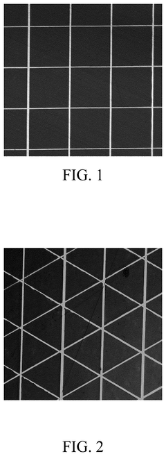
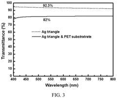
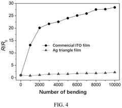
- A metal grid flexible transparent conductive film is developed, comprising a flexible substrate and a sputtered metal grid, specifically using a silver (Ag) grid with tunable microstructure and thickness to achieve optimal transparency and conductivity.
Manufacturing Processes and Scalability Challenges
The manufacturing of transparent conductive films (TCFs) for flexible display applications presents unique challenges that differ significantly from traditional rigid display production. Roll-to-roll (R2R) processing has emerged as the predominant manufacturing method for TCFs on flexible substrates, offering advantages in throughput and cost-effectiveness compared to batch processing. This continuous process allows for the deposition of conductive materials such as silver nanowires, carbon nanotubes, or PEDOT:PSS onto flexible polymer substrates at speeds reaching several meters per minute under optimized conditions.
Despite these advantages, R2R manufacturing faces several critical challenges. Maintaining uniform coating thickness across large areas remains problematic, with edge effects and substrate deformation during processing leading to performance variations. Current industrial implementations typically achieve thickness uniformity within ±5%, though premium applications require tighter tolerances of ±2% or better.
Material compatibility issues also present significant hurdles. The low temperature tolerance of polymer substrates (typically below 150°C) restricts processing options, eliminating many high-temperature annealing techniques used for traditional ITO on glass. This limitation has driven the development of alternative low-temperature curing methods, including photonic sintering, plasma treatment, and chemical approaches, each with their own efficiency-performance tradeoffs.
Scalability challenges extend beyond technical considerations to economic factors. The capital expenditure for establishing high-volume R2R production lines for TCFs can range from $10-50 million, depending on production capacity and technology sophistication. This substantial investment creates significant barriers to entry for smaller manufacturers and startups, contributing to market concentration among established players.
Yield management represents another critical challenge, with current industry benchmarks for high-quality TCF production typically ranging from 85-92%. Defects including pinholes, scratches, and conductivity variations can render significant portions of production unusable for premium display applications. Advanced in-line inspection systems utilizing machine vision and AI-based defect recognition have become essential components of modern production lines, though their implementation adds complexity and cost.
Environmental considerations are increasingly influencing manufacturing approaches. Traditional TCF production often involves hazardous chemicals and significant energy consumption. Recent innovations focus on developing water-based processing methods and ambient-temperature curing techniques that reduce environmental impact while maintaining performance specifications, though these approaches typically sacrifice some degree of conductivity or transparency.
Environmental Impact and Sustainability Considerations
The environmental impact of transparent conductive films (TCFs) in flexible display applications represents a critical consideration as the industry moves toward more sustainable manufacturing practices. Traditional indium tin oxide (ITO) films, while effective conductors, pose significant environmental challenges due to the scarcity of indium as a natural resource. Current estimates suggest that indium reserves may face depletion within the next few decades if consumption continues at present rates, highlighting the urgent need for alternative materials.
Manufacturing processes for TCFs typically involve energy-intensive methods such as sputtering, chemical vapor deposition, and high-temperature annealing. These processes contribute substantially to the carbon footprint of flexible display production. For instance, the energy consumption for ITO deposition can reach up to 2-3 kWh per square meter of film, resulting in considerable greenhouse gas emissions throughout the production lifecycle.
Chemical usage presents another environmental concern, particularly with wet etching processes that employ acids and other hazardous substances. These chemicals require careful handling and disposal to prevent environmental contamination. Additionally, the production of TCFs often involves solvents that can release volatile organic compounds (VOCs), contributing to air pollution and potential health risks for workers in manufacturing facilities.
Emerging alternatives such as silver nanowire networks, carbon nanotubes, and graphene-based films offer promising environmental advantages. These materials generally require less energy-intensive processing and reduce dependence on rare earth elements. For example, solution-processed silver nanowire films can be manufactured at lower temperatures, potentially reducing energy consumption by 40-60% compared to traditional ITO processing.
End-of-life considerations for flexible displays incorporating TCFs present recycling challenges due to the composite nature of these devices. The intimate integration of conductive films with polymeric substrates complicates material separation and recovery. Current recycling rates for display components remain below 20% globally, with most end-of-life products entering landfills or incineration streams.
Industry initiatives are increasingly focusing on developing closed-loop systems for TCF production and recycling. Several major manufacturers have implemented programs to recover indium from production waste and end-of-life products, achieving recovery rates of up to 70% in optimized processes. Additionally, design-for-recycling approaches are being explored to facilitate easier separation of display components at end-of-life.
Regulatory frameworks worldwide are evolving to address the environmental impacts of electronic components, including TCFs. The European Union's Restriction of Hazardous Substances (RoHS) directive and similar regulations in other regions are driving manufacturers toward more environmentally benign materials and processes, creating market incentives for sustainable innovation in the TCF space.
Unlock deeper insights with Patsnap Eureka Quick Research — get a full tech report to explore trends and direct your research. Try now!
Generate Your Research Report Instantly with AI Agent
Supercharge your innovation with Patsnap Eureka AI Agent Platform!