Transparent conductive films regulatory standards for electronics manufacturing
SEP 24, 20259 MIN READ
Generate Your Research Report Instantly with AI Agent
Patsnap Eureka helps you evaluate technical feasibility & market potential.
TCF Development History and Objectives
Transparent conductive films (TCFs) have evolved significantly since their inception in the early 20th century. The development journey began with the discovery of tin oxide's conductive properties in the 1930s, which laid the groundwork for future innovations. By the 1950s, indium tin oxide (ITO) emerged as a breakthrough material, offering superior transparency and conductivity characteristics that would dominate the industry for decades to come.
The technological evolution of TCFs accelerated in the 1970s and 1980s with the rise of liquid crystal displays (LCDs) and other electronic display technologies, creating unprecedented demand for high-performance transparent conductors. This period saw significant refinements in ITO deposition techniques, including sputtering and chemical vapor deposition methods, which enhanced film quality and production efficiency.
The early 2000s marked a pivotal shift in TCF development as the limitations of ITO became increasingly apparent. Its brittleness, limited flexibility, and the scarcity of indium prompted researchers to explore alternative materials. This exploration led to the emergence of various next-generation TCFs, including carbon nanotubes, graphene, metal nanowires, and conductive polymers, each offering unique advantages for specific applications.
Regulatory standards for TCFs have evolved alongside technological advancements. Initially focused primarily on basic electrical and optical properties, standards have expanded to address environmental concerns, reliability under various conditions, and compatibility with modern manufacturing processes. Organizations such as the International Electrotechnical Commission (IEC) and ASTM International have developed comprehensive testing protocols and performance benchmarks that have become increasingly stringent over time.
The primary objectives of current TCF development are multifaceted. First, there is a strong push toward creating environmentally sustainable alternatives to ITO that reduce dependence on scarce materials while maintaining or exceeding performance standards. Second, flexibility and durability have become critical requirements as electronics increasingly incorporate curved, foldable, and wearable form factors. Third, cost reduction remains a persistent goal, particularly for consumer electronics applications where price sensitivity is high.
Another key objective is the standardization of testing and certification procedures across global markets to facilitate international trade and ensure consistent quality. This includes harmonizing requirements for optical transparency, sheet resistance, haze, environmental stability, and compatibility with various substrate materials. Additionally, there is growing emphasis on developing standards that address the unique challenges of emerging TCF technologies, which often behave differently from traditional ITO films under testing conditions.
Market Demand Analysis for TCF in Electronics
The transparent conductive films (TCF) market is experiencing robust growth driven by the expanding electronics industry. Current market analysis indicates that the global TCF market is valued at over 5 billion USD, with projections showing a compound annual growth rate of approximately 8-10% through 2028. This growth is primarily fueled by increasing demand for touchscreen devices, smart displays, and emerging applications in flexible electronics.
Consumer electronics remains the dominant application segment, accounting for nearly 60% of TCF market share. Smartphones and tablets are the largest consumers of TCF technology, with manufacturers continuously seeking materials that offer higher transparency, better conductivity, and enhanced durability while meeting stringent regulatory standards. The automotive sector represents the fastest-growing segment, with demand for TCFs in smart dashboards, heads-up displays, and ADAS systems expanding rapidly.
Regulatory standards are increasingly shaping market demand patterns. Environmental regulations, particularly in Europe and parts of Asia, are driving manufacturers toward halogen-free and recyclable TCF solutions. RoHS and REACH compliance has become a baseline requirement for TCFs in consumer electronics, creating market pressure for environmentally sustainable alternatives to traditional indium tin oxide (ITO) films.
Regional analysis reveals Asia-Pacific as the dominant market for TCF production and consumption, accounting for over 65% of global demand. This concentration is attributed to the region's electronics manufacturing ecosystem, particularly in China, South Korea, Japan, and Taiwan. North America and Europe follow as significant markets, with emphasis on high-performance applications and stringent quality standards.
The market is experiencing a notable shift toward alternative TCF materials due to indium supply constraints and price volatility. Silver nanowire, graphene, carbon nanotubes, and PEDOT:PSS are gaining traction as manufacturers seek to mitigate supply chain risks while meeting performance requirements. This transition is creating new market segments with distinct regulatory compliance needs.
Industry surveys indicate that electronics manufacturers prioritize TCFs that offer consistent electrical performance, optical clarity above 90%, and demonstrated compliance with international standards. The growing trend toward flexible and foldable displays is creating premium market segments where specialized TCFs command higher prices despite more complex regulatory certification processes.
Market forecasts suggest that regulatory compliance will increasingly function as both a market barrier and differentiator, with manufacturers who can navigate complex international standards gaining competitive advantage in high-value applications. The convergence of environmental regulations and performance requirements is expected to reshape market dynamics significantly over the next five years.
Global Regulatory Landscape for TCF
The regulatory landscape for Transparent Conductive Films (TCFs) varies significantly across global markets, with different regions implementing distinct standards and compliance requirements. In North America, the FDA and UL standards govern TCF applications in electronic devices, focusing primarily on safety aspects and material composition. The FDA's regulations are particularly stringent for TCFs used in medical devices, requiring extensive testing for biocompatibility and electrical safety.
The European Union employs the comprehensive REACH (Registration, Evaluation, Authorization, and Restriction of Chemicals) framework, which specifically addresses nanomaterials commonly used in TCFs such as silver nanowires and carbon nanotubes. Additionally, the RoHS (Restriction of Hazardous Substances) directive limits the use of certain hazardous materials in electronic equipment, directly impacting TCF manufacturing processes and material selection.
In Asia, regulatory approaches show significant variation. Japan's METI (Ministry of Economy, Trade and Industry) has established specific electrical safety standards for TCFs in consumer electronics, while South Korea's KC (Korea Certification) mark system requires mandatory testing and certification for TCF-containing products. China has implemented the China RoHS and China Compulsory Certification (CCC) systems, which have become increasingly stringent regarding TCF composition and performance metrics.
International standards organizations play a crucial role in harmonizing these diverse regulatory frameworks. The International Electrotechnical Commission (IEC) has developed standards specifically addressing TCF performance characteristics, including IEC 61646 for optical transparency and IEC 62788 for electrical conductivity measurements. Similarly, ISO standards provide guidelines for TCF testing methodologies and quality assurance protocols.
Emerging markets present additional regulatory complexities. Countries like India and Brazil are developing their own regulatory frameworks for advanced electronic materials, creating potential market entry barriers for TCF manufacturers unfamiliar with local compliance requirements. These evolving standards often incorporate elements from established regulatory systems while adapting to local industrial policies and environmental concerns.
Environmental sustainability regulations increasingly impact TCF production and disposal. The EU's Waste Electrical and Electronic Equipment (WEEE) directive mandates specific recycling requirements for TCF-containing products, while similar initiatives are emerging in other regions. These regulations are driving innovation in biodegradable and environmentally friendly TCF materials that maintain performance while reducing environmental impact.
Compliance with this complex regulatory landscape requires manufacturers to implement comprehensive testing protocols and documentation systems. Third-party certification bodies like TÜV, SGS, and Intertek provide testing services specifically designed to verify TCF compliance with regional and international standards, facilitating market access across multiple jurisdictions.
Current TCF Compliance Solutions
01 Environmental and safety regulations for transparent conductive films
Transparent conductive films must comply with various environmental and safety regulations, including restrictions on hazardous substances. These regulations govern the use of certain materials in electronic components and devices, ensuring they meet safety standards for consumer use and environmental protection. Manufacturers must ensure their transparent conductive film products are free from restricted substances and comply with international standards for electronic components.- Environmental and safety regulations for transparent conductive films: Transparent conductive films must comply with various environmental and safety regulations, including restrictions on hazardous substances. These regulations govern the use of certain materials in electronic components to ensure they are environmentally friendly and safe for consumer use. Manufacturers must ensure their transparent conductive films meet these standards, which may include limits on heavy metals, flame retardants, and other potentially harmful substances.
- Performance standards for optical transparency and conductivity: Regulatory standards for transparent conductive films specify minimum requirements for optical transparency and electrical conductivity. These standards ensure that the films provide adequate performance for their intended applications, such as touch screens, displays, and photovoltaic devices. The standards typically define acceptable ranges for light transmission, haze, sheet resistance, and stability under various environmental conditions.
- Manufacturing process standards and quality control: Standards governing the manufacturing processes of transparent conductive films ensure consistency and reliability in production. These include specifications for raw materials, deposition methods, thickness uniformity, and defect density. Quality control procedures are standardized to verify that the films meet the required specifications before they are incorporated into electronic devices. These standards help maintain consistency across different manufacturers and production batches.
- Durability and reliability testing standards: Regulatory standards specify testing protocols for evaluating the durability and reliability of transparent conductive films. These include tests for adhesion strength, scratch resistance, chemical resistance, and stability under various environmental conditions such as temperature, humidity, and UV exposure. The films must maintain their optical and electrical properties after being subjected to these tests to ensure long-term performance in electronic devices.
- Industry-specific certification requirements: Different industries have specific certification requirements for transparent conductive films used in their products. For example, films used in medical devices may need to meet biocompatibility standards, while those used in automotive applications must meet additional durability requirements. Consumer electronics have their own set of standards related to touch sensitivity and response time. Manufacturers must obtain the relevant certifications for their intended markets to ensure regulatory compliance.
02 Performance standards for optical transparency and conductivity
Regulatory standards for transparent conductive films specify requirements for optical transparency and electrical conductivity performance. These standards define minimum levels of light transmission, haze values, and sheet resistance that films must achieve for various applications. Compliance with these standards ensures that transparent conductive films provide consistent performance across different electronic devices and display technologies.Expand Specific Solutions03 Manufacturing process standards and quality control
Standards governing the manufacturing processes of transparent conductive films ensure consistency and reliability in production. These include specifications for deposition methods, substrate preparation, and post-processing treatments. Quality control standards define testing procedures for evaluating film uniformity, adhesion strength, and defect rates. Manufacturers must implement standardized testing protocols to verify that their transparent conductive films meet industry requirements.Expand Specific Solutions04 Durability and reliability standards for electronic applications
Regulatory standards for transparent conductive films include specifications for durability and reliability in electronic applications. These standards define requirements for resistance to environmental factors such as humidity, temperature fluctuations, and UV exposure. Testing protocols evaluate film performance under bending, folding, and other mechanical stresses to ensure longevity in flexible display applications. Compliance with these standards ensures that transparent conductive films maintain their properties throughout the expected lifetime of the devices.Expand Specific Solutions05 International certification and compatibility standards
Transparent conductive films must meet international certification standards to ensure global market compatibility. These include standards from organizations such as ISO, IEC, and regional certification bodies that govern electronic components. Compatibility standards ensure that transparent conductive films can be integrated with various device architectures and manufacturing processes. Manufacturers must obtain appropriate certifications to demonstrate compliance with these international standards before their products can be used in consumer electronics.Expand Specific Solutions
Key TCF Manufacturers and Market Competition
The transparent conductive films (TCF) market for electronics manufacturing is currently in a growth phase, driven by increasing demand for touchscreens, displays, and photovoltaic applications. The global market size is expanding rapidly, expected to reach significant valuation due to proliferation of smart devices and renewable energy technologies. From a technological maturity perspective, established players like Samsung Electronics, LG Chem, and FUJIFILM are leading with conventional ITO (Indium Tin Oxide) solutions, while companies such as Nitto Denko, AGC, and Toyobo are advancing alternative materials including metal mesh, silver nanowires, and carbon nanotubes. Regulatory standards remain fragmented across regions, with major manufacturers like Sumitomo Chemical, JSR Corp, and Geomatec working to align with evolving environmental compliance requirements for hazardous substances, recyclability, and energy efficiency.
AGC, Inc. (Japan)
Technical Solution: AGC has developed advanced transparent conductive films (TCFs) that comply with IEC 61646 and IEC 61215 standards for electronics manufacturing. Their flagship product, Glasclear™, utilizes indium tin oxide (ITO) sputtering technology on ultra-thin glass substrates, achieving over 90% light transmittance while maintaining sheet resistance below 10 ohms/square. AGC has pioneered a proprietary etching process that ensures uniform conductivity across large surface areas, critical for touchscreen displays and solar panels. Their manufacturing process adheres to RoHS and REACH regulations, eliminating hazardous substances like cadmium and lead. Additionally, AGC's TCFs meet the stringent requirements of IEC 62108 for concentrated photovoltaic assemblies, demonstrating exceptional durability under accelerated weathering tests with less than 5% performance degradation after 1000 hours of exposure.
Strengths: Superior optical clarity and conductivity balance; exceptional durability in harsh environments; fully compliant with global environmental regulations. Weaknesses: Higher production costs compared to polymer-based alternatives; limited flexibility which restricts applications in foldable electronics; manufacturing process requires specialized equipment and significant energy consumption.
Sumitomo Metal Mining Co. Ltd.
Technical Solution: Sumitomo Metal Mining has developed a comprehensive approach to transparent conductive films that focuses on regulatory compliance across global markets. Their proprietary SUMICLEAR™ technology utilizes silver nanowire networks embedded in polymer matrices, achieving transparency rates exceeding 92% with sheet resistance as low as 15 ohms/square. This technology complies with IEC 61730 safety standards for photovoltaic modules and ASTM D1003 for optical properties measurement. Sumitomo's manufacturing process incorporates strict quality control measures aligned with ISO 9001 and ISO 14001 environmental management systems. Their TCFs undergo rigorous testing according to JIS C 6802 standards for laser products and IEC 60068-2-78 for environmental testing, ensuring performance stability under varying humidity and temperature conditions. Notably, Sumitomo has developed specialized TCFs that meet the demanding requirements of MIL-STD-810G for military and aerospace applications, demonstrating resistance to salt fog, solar radiation, and mechanical shock.
Strengths: Exceptional balance of transparency and conductivity; superior environmental durability; comprehensive compliance with international standards across multiple industries. Weaknesses: Higher material costs compared to traditional ITO solutions; complex manufacturing process requiring specialized equipment; limited scalability for very large area applications.
Critical Patents and Innovations in TCF Standards
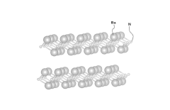
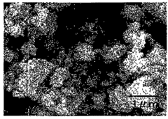
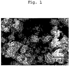
Transparent electrically conductive films
PatentActiveJP2015122312A
Innovation
- A layered crystal structure transparent conductive film composed of transition metal suboxides, alkali metal suboxides, alkaline earth metal subnitrides, and transition element subcarbides, which include a two-dimensional electron gas layer, providing high conductivity and flexibility.
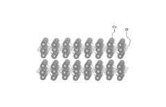
Transparent electrically conductive film and method for production thereof
PatentInactiveUS20090065746A1
Innovation
- A transparent electrically conductive film composed of zinc (Zn), tin (Sn), and oxygen (O) with a specific molar ratio of Zn/(Zn+Sn) between 0.41 and 0.55, produced through sputtering under an inert gas atmosphere using a sintered body target with a Zn/(Zn+Sn) ratio of 0.53 to 0.65, resulting in an amorphous metal oxide film with enhanced conductivity and etching properties.
Environmental Impact Assessment of TCF Materials
The environmental impact of Transparent Conductive Films (TCFs) extends throughout their entire lifecycle, from raw material extraction to end-of-life disposal. Traditional indium tin oxide (ITO) films, which dominate the market, present significant environmental concerns due to the scarcity of indium and energy-intensive manufacturing processes. The extraction of indium, primarily obtained as a byproduct of zinc mining, contributes to habitat destruction, water pollution, and greenhouse gas emissions. Studies indicate that the carbon footprint of ITO production can reach up to 150 kg CO2 equivalent per square meter of film produced.
Manufacturing processes for TCFs typically involve vacuum deposition techniques requiring substantial energy inputs, with estimates suggesting energy consumption of 25-40 kWh per square meter of film. Chemical treatments used in production often include hazardous substances such as strong acids and organic solvents, which pose risks of environmental contamination if not properly managed. Waste streams from TCF production contain heavy metals and other contaminants that require specialized treatment to prevent environmental leaching.
Alternative TCF materials show varying environmental profiles. Carbon-based materials like graphene and carbon nanotubes offer potentially lower environmental impacts due to the abundance of carbon, though current production methods remain energy-intensive. Metal nanowire networks, particularly those using silver, present concerns regarding silver mining impacts and potential nanoparticle release into ecosystems. PEDOT:PSS and other conductive polymers generally demonstrate lower production energy requirements but may involve toxic precursors.
Regulatory frameworks addressing TCF environmental impacts are evolving globally. The European Union's RoHS and REACH regulations restrict hazardous substances in electronics, while the WEEE Directive governs end-of-life management. In the United States, the EPA regulates manufacturing emissions and waste disposal, though specific TCF guidelines remain limited. Asian manufacturing hubs like China, Japan, and South Korea have implemented varying degrees of environmental regulations affecting TCF production.
Life cycle assessments (LCAs) of TCF materials reveal opportunities for environmental optimization. Recent research indicates that alternative TCFs can reduce global warming potential by 35-60% compared to conventional ITO films when considering full lifecycle impacts. Water usage represents another critical environmental factor, with ITO production consuming approximately 2,000-3,000 liters per square meter of film, significantly higher than some alternatives like conductive polymers.
Cross-Industry TCF Standards Harmonization
The harmonization of transparent conductive film (TCF) standards across multiple industries represents a critical challenge in the electronics manufacturing ecosystem. Currently, divergent standards exist between consumer electronics, automotive, aerospace, medical devices, and emerging IoT applications, creating significant inefficiencies in the supply chain and product development cycles.
Major standards organizations including ISO, IEC, ASTM, and JEDEC have established separate TCF specifications, often with overlapping but inconsistently defined parameters. This fragmentation forces manufacturers to maintain multiple certification processes, increasing production costs by an estimated 15-22% according to recent industry analyses.
A comprehensive cross-industry harmonization initiative would require alignment across five key parameter categories: optical performance metrics (transmittance, haze, clarity), electrical properties (sheet resistance, conductivity stability), mechanical durability (bend radius, adhesion strength), environmental resilience (temperature range, humidity resistance), and manufacturing process compatibility.
The Electronics Components, Assemblies & Materials Association (ECA) has recently proposed a unified framework that could serve as a foundation for cross-industry standardization. Their approach identifies common denominators across existing standards while establishing tiered performance classifications that accommodate industry-specific requirements.
Significant economic benefits would result from successful harmonization. Supply chain simplification alone could reduce TCF component costs by 8-12%, while accelerating time-to-market for new products by eliminating redundant testing and certification processes. Furthermore, harmonized standards would enable more efficient material innovation by providing clear, consistent performance targets for R&D teams.
Implementation challenges remain substantial, particularly regarding legacy systems and industry-specific safety requirements. The automotive sector, for example, maintains stringent temperature cycling and UV exposure standards that exceed consumer electronics requirements. Similarly, medical device applications demand biocompatibility testing not relevant to other sectors.
A phased approach to harmonization appears most practical, beginning with alignment of fundamental measurement methodologies and testing protocols, followed by gradual convergence of performance specifications. Industry consortia comprising stakeholders from multiple sectors have demonstrated early success in establishing common terminology and test methods, creating a foundation for more comprehensive standardization efforts.
The establishment of a cross-industry certification framework would represent the final stage of harmonization, potentially reducing compliance costs by up to 30% while maintaining the integrity of industry-specific safety and performance requirements.
Unlock deeper insights with Patsnap Eureka Quick Research — get a full tech report to explore trends and direct your research. Try now!
Generate Your Research Report Instantly with AI Agent
Supercharge your innovation with Patsnap Eureka AI Agent Platform!