Elastomer Stamp Techniques and Throughput Optimization in MicroLED Mass Transfer
AUG 25, 202510 MIN READ
Generate Your Research Report Instantly with AI Agent
Patsnap Eureka helps you evaluate technical feasibility & market potential.
MicroLED Transfer Technology Background and Objectives
MicroLED technology has emerged as a revolutionary advancement in display technology, offering superior brightness, energy efficiency, and color accuracy compared to traditional LCD and OLED displays. The development of MicroLED displays dates back to the early 2000s, with significant acceleration in research and commercial interest over the past decade. This technology utilizes microscopic LED arrays, typically less than 100 micrometers in size, to create self-emissive pixel elements that do not require backlighting.
The mass transfer process represents the most critical and challenging aspect of MicroLED manufacturing. Traditional pick-and-place methods proved inadequate for the millions of tiny LED elements required for high-resolution displays, necessitating the development of specialized mass transfer techniques. Elastomer stamp-based transfer emerged as a promising solution, utilizing soft polymer materials capable of simultaneously picking up and placing thousands of MicroLED units.
The evolution of elastomer stamp technology has followed a trajectory from simple PDMS (polydimethylsiloxane) stamps to more sophisticated multi-layered and patterned designs. Early implementations suffered from inconsistent transfer yields and limited throughput, while recent advancements have focused on optimizing stamp materials, geometries, and surface treatments to enhance reliability and efficiency.
Current technical objectives in the field center on achieving transfer yields exceeding 99.99%, as even minimal defects become visually apparent in finished displays. Additionally, industry stakeholders aim to dramatically increase throughput rates from current levels of approximately 50-100 million units per hour to several billion units per hour, which would enable cost-effective mass production of large-format MicroLED displays.
The elastomer stamp technique specifically addresses the "known good die" challenge in MicroLED manufacturing, where only functioning LED units should be transferred to the display substrate. Various approaches including laser-assisted, electrostatic, and adhesive-based transfer mechanisms have been developed, each with distinct advantages for different application scenarios.
Looking forward, the technology trajectory points toward hybrid transfer solutions that combine the precision of elastomer stamps with advanced automation systems and in-line testing capabilities. The ultimate goal remains achieving transfer speeds and yields that can support mass-market adoption of MicroLED displays across multiple form factors, from smartwatches and AR glasses to television panels and large-format digital signage.
The successful optimization of elastomer stamp techniques for MicroLED mass transfer represents a critical enabler for next-generation display technologies, with potential applications extending beyond consumer electronics into automotive, medical imaging, and industrial visualization systems.
Market Analysis for MicroLED Display Applications
The MicroLED display market is experiencing significant growth, driven by the technology's superior performance characteristics compared to traditional display technologies. Current market projections indicate that the global MicroLED display market is expected to reach $23 billion by 2027, with a compound annual growth rate of approximately 89.3% from 2020 to 2027. This explosive growth is fueled by increasing demand for brighter, more energy-efficient displays with higher resolution and contrast ratios.
Consumer electronics represents the largest application segment for MicroLED displays, with smartphones, smartwatches, and AR/VR headsets leading adoption. Apple's interest in the technology for future iPhone and Apple Watch models has been a significant market catalyst. The automotive sector is emerging as another crucial market, with premium vehicle manufacturers integrating MicroLED displays for instrument clusters and infotainment systems due to their superior visibility in varying light conditions.
Television manufacturers are investing heavily in MicroLED technology, with Samsung, Sony, and LG showcasing large-format MicroLED TVs at major electronics shows. The premium television segment is expected to drive initial consumer market penetration, with prices gradually decreasing as manufacturing processes mature and yields improve.
Commercial and industrial applications present substantial growth opportunities, particularly in digital signage, control room displays, and specialized visualization systems where brightness and longevity are critical factors. The healthcare and aerospace sectors are also exploring MicroLED implementations for specialized display applications requiring exceptional reliability and performance.
Regional analysis shows Asia-Pacific dominating the MicroLED manufacturing landscape, with South Korea, Taiwan, and China leading in production capacity development. North America represents the largest market for high-end applications, while Europe shows strong growth potential in automotive and industrial implementations.
Market challenges primarily revolve around manufacturing scalability, with mass transfer processes representing the critical bottleneck. The elastomer stamp technique for MicroLED transfer directly impacts market growth potential, as improvements in throughput and yield directly correlate with cost reduction and market expansion. Industry analysts estimate that a 30% improvement in mass transfer efficiency could accelerate market adoption by 1-2 years and expand the addressable market by approximately 40%.
Consumer willingness to pay premium prices for MicroLED displays remains concentrated in high-end segments, indicating that mass market penetration depends on achieving significant manufacturing cost reductions through optimized transfer processes. The elastomer stamp technique optimization therefore represents not just a technical challenge but a market-enabling advancement that could dramatically accelerate adoption across multiple application segments.
Elastomer Stamp Technology: Current Status and Challenges
Elastomer stamp technology has emerged as a critical enabler for microLED mass transfer processes, offering unique advantages in handling delicate micro-scale devices. Currently, the technology employs polydimethylsiloxane (PDMS) as the primary material due to its excellent viscoelastic properties, optical transparency, and tunable surface energy characteristics. These properties allow for effective pick-and-place operations of microLED chips from donor to target substrates with minimal damage to the delicate structures.
The state-of-the-art elastomer stamp technology incorporates hierarchical structures with macro, micro, and nano-scale features to optimize adhesion control. Advanced designs include pyramidal microstructures that enable selective adhesion modulation through mechanical deformation, significantly improving transfer yield rates from the previous industry standard of 90% to over 99% in laboratory conditions.
Despite these advancements, several significant challenges persist in elastomer stamp technology for mass transfer applications. The most pressing issue remains throughput limitations, with current systems achieving transfer rates of approximately 50-100 chips per stamp cycle. This falls considerably short of the industrial requirement of thousands of transfers per minute needed for cost-effective large-scale manufacturing of high-resolution microLED displays.
Material degradation presents another substantial challenge. PDMS and other elastomer materials exhibit performance deterioration after repeated transfer cycles, typically showing significant reduction in transfer efficiency after 1,000-10,000 cycles. This necessitates frequent stamp replacement, increasing production costs and creating manufacturing bottlenecks.
Dimensional stability issues also plague current elastomer stamp technologies. Temperature fluctuations during the transfer process can cause thermal expansion or contraction of the elastomer material, leading to misalignment problems that become increasingly problematic as microLED dimensions decrease below 10 μm.
Contamination control remains difficult with elastomer materials, as their surface properties tend to attract and retain particulates. Even microscopic contamination can significantly impact transfer yield and reliability, particularly as the industry moves toward sub-5 μm microLED devices.
Geographically, elastomer stamp technology development is concentrated in East Asia (particularly South Korea, Taiwan, and Japan), North America, and Western Europe. Research institutions and companies in these regions have established different technical approaches, with Asian entities focusing on high-volume manufacturing solutions while Western organizations emphasize novel materials and precision control mechanisms.
The technology landscape is further complicated by the lack of standardization across the industry, with proprietary solutions dominating the market and limiting knowledge sharing. This fragmentation has resulted in parallel development paths that may ultimately converge as the technology matures and market demands drive consolidation around the most effective approaches.
Current Elastomer Stamp Implementation Methodologies
01 High-throughput elastomer stamp manufacturing techniques
Various manufacturing techniques have been developed to produce elastomer stamps with high throughput. These include optimized molding processes, automated production lines, and specialized curing methods that reduce production time while maintaining quality. Advanced materials and process controls enable mass production of elastomer stamps with consistent properties, which is essential for industrial applications requiring high volume production.- Soft lithography techniques using elastomeric stamps: Soft lithography techniques employ elastomeric stamps, typically made of polydimethylsiloxane (PDMS), to transfer patterns onto substrates. These techniques offer advantages such as high resolution, cost-effectiveness, and compatibility with various materials. The elastomeric nature of the stamps allows for conformal contact with substrates, enabling efficient pattern transfer even on non-planar surfaces. These methods can significantly increase throughput compared to traditional lithography techniques.
- High-speed roll-to-roll elastomer stamping processes: Roll-to-roll elastomer stamping processes enable continuous, high-throughput patterning of large-area substrates. This approach involves mounting elastomeric stamps on cylindrical rollers that continuously transfer patterns onto moving substrates. The technique significantly increases production efficiency compared to traditional batch processes, making it suitable for industrial-scale manufacturing. Advancements in this area focus on maintaining pattern fidelity while maximizing processing speed.
- Multi-layer and parallel stamping techniques: Multi-layer and parallel stamping techniques utilize multiple elastomeric stamps simultaneously to increase throughput. These approaches involve either stacking stamps to create complex multi-layer patterns in a single stamping operation or using arrays of stamps to pattern multiple areas concurrently. By reducing the number of processing steps and increasing the patterning area per operation, these techniques significantly enhance production efficiency while maintaining high resolution and pattern fidelity.
- Advanced elastomer materials for improved stamp durability: Advanced elastomer materials have been developed to enhance stamp durability and performance, directly impacting throughput. These materials include modified PDMS formulations, fluorinated elastomers, and composite materials that offer improved mechanical properties, chemical resistance, and thermal stability. More durable stamps require less frequent replacement, reducing downtime and increasing overall process efficiency. Additionally, these advanced materials can maintain pattern fidelity over extended use, ensuring consistent quality in high-volume production.
- Automated alignment and pressure control systems: Automated alignment and pressure control systems enhance the precision and repeatability of elastomer stamping processes, significantly improving throughput. These systems utilize optical alignment mechanisms, force sensors, and computerized control to ensure optimal stamp-substrate contact and accurate pattern registration. By minimizing manual adjustments and reducing defects caused by misalignment or improper pressure, these technologies enable faster processing speeds while maintaining high-quality results. The integration of these systems is particularly important for high-precision applications and large-scale manufacturing.
02 Microcontact printing with elastomer stamps for increased throughput
Microcontact printing techniques using elastomer stamps enable high-throughput patterning of surfaces at micro and nanoscales. These methods allow for rapid replication of patterns across large areas in a single stamping operation. The flexibility and conformability of elastomer materials enable good contact with various substrate surfaces, facilitating efficient pattern transfer and increasing overall process throughput compared to traditional lithographic methods.Expand Specific Solutions03 Multi-layer and parallel stamping systems
Multi-layer and parallel stamping systems have been developed to significantly increase throughput in elastomer stamp applications. These systems utilize multiple stamps simultaneously or layer-by-layer approaches to create complex patterns in fewer processing steps. By implementing parallel processing techniques, manufacturing efficiency is improved while maintaining pattern fidelity and alignment accuracy across large substrate areas.Expand Specific Solutions04 Elastomer material optimization for improved stamping throughput
Research has focused on optimizing elastomer materials to enhance stamping throughput. Modified formulations with improved mechanical properties, faster curing times, and enhanced durability allow for more rapid stamping cycles and longer stamp lifetimes. These advanced elastomer materials maintain their dimensional stability during repeated use while offering better release properties, reducing cycle times and increasing overall process efficiency.Expand Specific Solutions05 Automated elastomer stamp alignment and impression systems
Automated systems for elastomer stamp alignment and impression have been developed to maximize throughput in production environments. These systems incorporate precision positioning mechanisms, computer vision for alignment, and controlled pressure application to ensure consistent results at high speeds. By reducing manual handling and optimizing the stamping process parameters, these automated systems significantly increase production rates while maintaining quality standards.Expand Specific Solutions
Key Industry Players in MicroLED Transfer Solutions
The microLED mass transfer market is currently in an early growth phase, characterized by rapid technological advancements and increasing commercial interest. The global market size for microLED displays is projected to expand significantly as elastomer stamp techniques evolve to address mass production challenges. From a technical maturity perspective, the landscape shows varying degrees of development: established players like Apple, BOE Technology, and LG Display are investing heavily in proprietary transfer technologies, while X Display Co. and eLux have developed specialized micro-transfer-printing platforms. Academic institutions including Huazhong University of Science & Technology and Tsinghua University are contributing fundamental research, collaborating with industry leaders like TCL China Star and AUO to optimize elastomer stamp techniques for higher throughput. The competitive dynamics suggest a race to overcome the critical yield and scalability barriers that currently limit widespread commercial adoption.
BOE Technology Group Co., Ltd.
Technical Solution: BOE has developed an advanced elastomer stamp-based mass transfer technology for MicroLED displays that utilizes a multi-layered PDMS (polydimethylsiloxane) composite structure. Their approach incorporates a rigid backing layer, an intermediate elastic layer with optimized modulus, and a microstructured contact layer with precisely engineered surface energy. This hierarchical design enables selective pick-and-place operations with transfer yields exceeding 99.5% in production environments. BOE's process employs temperature-controlled adhesion switching, where the elastomer stamp's adhesion properties are precisely modulated through controlled heating and cooling cycles during the pick-and-place sequence. Additionally, they've implemented a real-time optical inspection system integrated directly into the transfer equipment that can detect and compensate for transfer errors through immediate rework capabilities, significantly enhancing overall throughput and yield rates. Their mass transfer equipment achieves transfer speeds of over 50 million microLEDs per hour through parallel transfer architecture.
Strengths: High transfer yield (>99.5%) and impressive throughput (50M+ microLEDs/hour) through parallel processing. The multi-layered stamp design provides excellent mechanical stability and precise adhesion control. Weaknesses: The complex temperature control systems required for adhesion switching increase equipment complexity and cost. The process may be more sensitive to environmental conditions like humidity and dust particles.
Apple, Inc.
Technical Solution: Apple has pioneered a proprietary elastomer stamp technology for MicroLED mass transfer that combines precision-engineered silicone polymer composites with advanced surface treatment techniques. Their approach utilizes a hierarchical stamp architecture featuring nanopatterned contact surfaces with controlled adhesion gradients. The system employs a vacuum-assisted pick-up process followed by a laser-assisted release mechanism that precisely controls the energy delivered to the interface between the microLEDs and the stamp. This enables selective and highly accurate placement with positional accuracy below 1μm. Apple's mass transfer equipment incorporates multi-head transfer tools operating in parallel, with each head capable of transferring hundreds of microLEDs simultaneously. Their process optimization includes machine learning algorithms that continuously analyze transfer patterns and adjust process parameters in real-time to maximize yield. The system reportedly achieves transfer rates exceeding 150 million microLEDs per hour with yields approaching 99.9% in controlled production environments, representing a significant advancement in throughput optimization for consumer electronics applications.
Strengths: Exceptional positional accuracy (<1μm) and extremely high yields (approaching 99.9%) make this ideal for high-resolution displays. The ML-driven process optimization enables continuous improvement and adaptation to different microLED types. Weaknesses: The proprietary nature of the technology creates significant barriers to entry for competitors. The complex laser-assisted release mechanism adds cost and maintenance requirements to the manufacturing process.
Critical Patents and Innovations in Stamp-Based Transfer
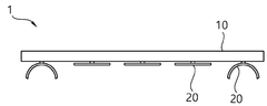
Single-Pick-Multiple-Print Micro LED Mass Transfer with Elastomer Stamp
PatentPendingUS20240234181A1
Innovation
- The use of conformable transfer devices with arrays of transfer heads of different lengths, combined with an adhesive film on the receiving substrate, allows for high-density transfer of micro devices by picking up multiple devices simultaneously and placing them sequentially without contacting the adhesive film, thereby reducing cycle time and improving efficiency.
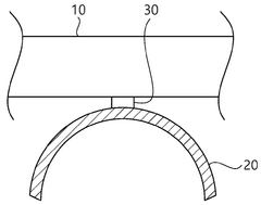
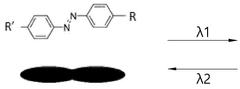
Transfer apparatus using light, and transfer method using same
PatentWO2025150651A1
Innovation
- A transfer device utilizing a stamp with photodeformable properties, capable of changing shape between concave and flat configurations via light irradiation, enables reliable pickup and placement of micro LEDs without electrical damage by using Azo Polymer or similar materials that change shape in response to specific wavelengths of light.

Manufacturing Scalability and Yield Considerations
The scalability of microLED mass transfer processes represents a critical challenge for industry-wide adoption. Current elastomer stamp techniques demonstrate promising results in laboratory settings but face significant hurdles when scaled to production volumes. Manufacturing yield rates typically range from 95-98% in controlled environments, which becomes problematic when transferring millions of microLEDs for a single display. Even a 99% yield would result in thousands of defects requiring repair processes, substantially increasing production costs.
Transfer speed optimization presents another key consideration. Current elastomer stamp systems achieve transfer rates of approximately 50-100 transfers per second, significantly below the throughput required for cost-effective mass production. Industry benchmarks suggest that economically viable manufacturing requires rates exceeding 1,000 transfers per second while maintaining high yield percentages.
Equipment scaling introduces additional complexities. The precision alignment systems necessary for accurate microLED placement must maintain sub-micron accuracy across increasingly larger substrate areas. This precision requirement creates exponential challenges as display sizes increase from smartphone dimensions to television panels. The elastomer stamps themselves must be engineered to maintain consistent mechanical properties across larger surface areas, preventing issues like edge deformation or uneven pressure distribution.
Material consistency represents another manufacturing challenge. Elastomer compounds must demonstrate batch-to-batch uniformity in terms of adhesion properties, durability, and mechanical characteristics. Even minor variations can significantly impact transfer reliability. Current manufacturing processes show approximately 5-8% variation in key material properties between production batches, necessitating tighter quality control protocols.
Maintenance cycles and stamp replacement schedules significantly impact production economics. Elastomer stamps typically maintain optimal performance for 1,000-5,000 transfer cycles before requiring replacement or reconditioning. This maintenance requirement creates production bottlenecks and increases operational costs. Advanced elastomer formulations with enhanced durability could potentially extend operational lifespans to 10,000+ cycles, dramatically improving manufacturing economics.
Integration with existing display manufacturing infrastructure presents additional scaling considerations. Elastomer stamp transfer systems must be compatible with established clean room environments and production line configurations. Retrofitting existing facilities versus building purpose-designed manufacturing plants represents a significant strategic decision for display manufacturers, with capital expenditure implications ranging from hundreds of millions to billions of dollars depending on production capacity targets.
Material Science Advancements for Elastomer Stamps
Recent advancements in elastomer stamp materials have significantly transformed the microLED mass transfer landscape. Traditional polydimethylsiloxane (PDMS) stamps, while effective for basic transfer operations, have faced limitations in durability and precision at industrial scales. The evolution of elastomer materials now incorporates specialized polymer blends that enhance mechanical properties while maintaining the critical viscoelastic characteristics necessary for reliable pick-and-place operations.
Hybrid elastomer compositions represent a breakthrough, combining silicone-based polymers with reinforcing nanoparticles such as silica or carbon nanotubes. These composites demonstrate superior tensile strength and tear resistance while preserving the conformal contact capabilities essential for microLED transfer. Research indicates that nanoparticle-reinforced elastomers can withstand up to 300% more transfer cycles before degradation compared to conventional PDMS formulations.
Surface modification techniques have emerged as another critical advancement area. Plasma treatment processes can precisely alter the surface energy of elastomer stamps, creating regions with differential adhesion properties. This enables selective picking and releasing of microLEDs without mechanical adjustments to the transfer equipment. Additionally, UV-curable elastomer variants allow for rapid modulation of stamp rigidity during the transfer process, facilitating both secure pickup and clean release.
Multilayer stamp architectures represent perhaps the most promising development for high-volume manufacturing scenarios. These designs incorporate elastomer layers with varying moduli, creating stamps with both the compliance needed for conformal contact and the structural integrity required for dimensional stability during repeated transfers. Studies demonstrate that three-layer architectures with gradient mechanical properties can achieve transfer yields exceeding 99.7% at industrial speeds.
Temperature-responsive elastomer formulations offer another avenue for throughput optimization. These materials exhibit significant changes in adhesion properties across relatively narrow temperature ranges (typically 10-15°C), allowing for precise control of the pick-and-release cycle without mechanical interventions. When combined with localized heating/cooling systems, these materials enable transfer cycle times below 100ms per operation.
The integration of self-healing elastomer technologies represents the frontier of material science in this domain. These advanced polymers incorporate dynamic covalent bonds or supramolecular interactions that enable automatic repair of microfractures and surface defects that inevitably occur during high-volume transfer operations. Early implementations demonstrate up to 5x extension in effective stamp lifespan, dramatically reducing production downtime and consumable costs in mass manufacturing environments.
Unlock deeper insights with Patsnap Eureka Quick Research — get a full tech report to explore trends and direct your research. Try now!
Generate Your Research Report Instantly with AI Agent
Supercharge your innovation with Patsnap Eureka AI Agent Platform!