Redundancy Pixel Mapping and Rework Flows in MicroLED Repair
AUG 25, 20259 MIN READ
Generate Your Research Report Instantly with AI Agent
Patsnap Eureka helps you evaluate technical feasibility & market potential.
MicroLED Repair Technology Background and Objectives
MicroLED technology has emerged as a revolutionary display technology over the past decade, promising superior performance compared to traditional LCD and OLED displays. The technology utilizes microscopic light-emitting diodes, typically smaller than 100 micrometers, to create self-emissive pixel elements with exceptional brightness, contrast, and energy efficiency. Since its conceptualization in the early 2000s, MicroLED has been positioned as the next generation display technology with potential applications ranging from smartwatches and smartphones to large-scale televisions and augmented reality devices.
The evolution of MicroLED technology has been marked by significant challenges in manufacturing, particularly in achieving high yield rates during production. One of the most critical challenges has been addressing defective pixels, which can severely impact display quality and production economics. As pixel densities increase and pixel sizes decrease, the probability of defects rises exponentially, making repair technologies essential for commercial viability.
Redundancy Pixel Mapping and Rework Flows represent a sophisticated approach to addressing these manufacturing challenges. This technology involves the strategic implementation of redundant pixels within the display architecture and the development of systematic processes to identify, map, and repair defective pixels. The concept evolved from early repair methods that relied on complete replacement of defective components to more efficient approaches that leverage redundancy and targeted rework.
The primary technical objective of MicroLED repair technology is to achieve near-perfect yield rates by implementing cost-effective repair strategies that maintain display quality while minimizing production costs. Specifically, the technology aims to develop automated systems capable of detecting defects at the microscopic level, mapping these defects in relation to redundant pixels, and executing precise repair operations without compromising the integrity of surrounding functional elements.
Current technological trajectories indicate a growing emphasis on AI-driven defect detection and repair planning, alongside advancements in micro-manipulation tools capable of operating at increasingly smaller scales. The industry is moving toward fully automated repair systems that can process large volumes of displays with minimal human intervention, significantly reducing production costs and increasing throughput.
The ultimate goal of this technology is to enable mass production of MicroLED displays across various size formats, from micro-displays for AR/VR applications to large-format televisions, by solving the yield challenges that have historically limited commercial adoption. Success in this domain would represent a significant milestone in display technology, potentially catalyzing widespread market adoption of MicroLED displays and enabling new applications previously constrained by technical limitations.
Market Analysis for MicroLED Display Repair Solutions
The global MicroLED display market is experiencing significant growth, with repair solutions becoming increasingly critical as adoption rates rise. Current market valuations place the MicroLED display sector at approximately 2.3 billion USD in 2023, with projections indicating a compound annual growth rate (CAGR) of 63.7% through 2030. Within this expanding market, repair solutions specifically addressing redundancy pixel mapping and rework flows are emerging as a crucial sub-segment.
Consumer electronics represents the largest application segment for MicroLED repair technologies, accounting for roughly 42% of the market share. This is primarily driven by the integration of MicroLED displays in premium smartphones, smartwatches, and AR/VR headsets where pixel perfection is paramount. The automotive sector follows as the second-largest market, growing at 71.2% CAGR as luxury vehicle manufacturers increasingly adopt MicroLED dashboard and entertainment displays.
Geographically, East Asia dominates the MicroLED repair solutions market with approximately 58% market share, largely due to the concentration of display manufacturing facilities in South Korea, Taiwan, and China. North America accounts for 24% of the market, primarily driven by research institutions and technology companies developing advanced repair methodologies.
The demand for sophisticated repair solutions is directly correlated with MicroLED's inherent manufacturing challenges. Current yield rates in MicroLED production range between 60-75%, significantly lower than mature LCD and OLED technologies. This yield gap creates a market opportunity valued at approximately 780 million USD specifically for repair technologies.
Key market drivers include the increasing resolution demands of next-generation displays, with 4K and 8K panels requiring near-perfect pixel functionality. Additionally, the expansion of MicroLED into larger display formats (above 100 inches) has amplified the economic impact of defective pixels, making repair solutions more cost-effective than panel replacement.
Market analysis reveals a significant price sensitivity threshold: repair solutions must keep costs below 15% of total panel production expenses to maintain economic viability. Current redundancy mapping and rework technologies add between 8-22% to production costs, indicating room for optimization and innovation.
Customer requirements are evolving toward automated repair systems that can be integrated directly into production lines, with 76% of manufacturers expressing preference for solutions that can be implemented without disrupting existing workflows. Speed of repair is another critical factor, with market leaders demanding systems capable of addressing multiple pixel defects within 30-45 seconds per panel.
Current Challenges in MicroLED Redundancy Implementation
Despite significant advancements in MicroLED technology, implementing effective redundancy systems faces several critical challenges. The primary obstacle lies in the complex pixel mapping algorithms required to seamlessly integrate redundant pixels when primary pixels fail. Current mapping techniques struggle with real-time decision-making processes that must determine which redundant pixel to activate and how to reconfigure the display matrix without creating visible artifacts or disrupting display uniformity.
The miniaturization of MicroLED displays compounds these challenges, as the physical space for implementing redundant pixels becomes increasingly constrained. Engineers must balance the need for adequate redundancy against the demand for higher pixel densities and resolution, creating a fundamental design tension that remains unresolved in many applications.
Power management presents another significant hurdle, as redundancy systems inherently increase the overall power requirements of MicroLED displays. The additional circuitry needed to support redundant pixels and their switching mechanisms can lead to thermal management issues, particularly in compact devices where heat dissipation is already problematic.
Yield management during manufacturing represents a persistent challenge, as the implementation of redundancy systems requires more complex production processes and testing protocols. The additional components and connections increase the potential failure points, potentially offsetting some of the yield improvements that redundancy systems are designed to provide.
From a software perspective, the control systems for managing redundancy must be sophisticated enough to detect pixel failures accurately and activate appropriate replacements without introducing latency or visual discontinuities. Current algorithms struggle to achieve this seamlessly, particularly in high-refresh-rate applications where even minor delays become noticeable.
Cost considerations remain a significant barrier to widespread implementation of robust redundancy systems. The additional materials, manufacturing complexity, and testing requirements substantially increase production costs, making comprehensive redundancy approaches economically unfeasible for many consumer applications.
Integration challenges also exist between the redundancy systems and repair workflows. Current rework flows often require manual intervention or specialized equipment that cannot easily interface with automated redundancy mapping systems, creating inefficiencies in the repair process and limiting the effectiveness of the overall yield improvement strategy.
Current Redundancy Pixel Mapping Techniques
01 Memory redundancy and repair techniques
Memory devices employ redundancy techniques to replace defective memory cells with spare elements. This involves mapping defective pixels or memory cells to redundant elements, improving yield and reliability. Advanced algorithms identify defective cells during testing and program fuse elements to redirect access from defective to redundant cells, enhancing repair efficiency in semiconductor memory manufacturing.- Memory redundancy and repair techniques: Memory devices employ redundancy techniques to replace defective memory cells with spare elements. This involves mapping defective pixels or memory cells to redundant elements, improving yield and reliability. Advanced repair algorithms identify optimal replacement patterns to maximize repair efficiency, while specialized circuits facilitate the remapping process during manufacturing or in-field operation.
- Display panel pixel repair methods: Display technologies utilize redundancy mapping to address defective pixels in panels. These methods involve identifying faulty pixels through testing procedures and rerouting signals to redundant elements. The repair flows include automated detection systems that map defect locations and implement repair strategies to maintain display quality and performance, significantly improving manufacturing yield for display panels.
- Semiconductor device repair efficiency optimization: Techniques for optimizing repair efficiency in semiconductor devices focus on streamlining the rework flow process. This includes developing algorithms that prioritize critical defects, implementing parallel repair operations, and utilizing statistical analysis to predict failure patterns. Advanced mapping techniques help identify the most efficient repair sequence, reducing repair time and increasing overall production throughput.
- Real-time defect detection and repair systems: Real-time systems for defect detection and repair incorporate continuous monitoring capabilities that identify pixel or memory cell failures during operation. These systems use dynamic redundancy mapping to reroute functions away from defective elements without interrupting device operation. The approach includes automated testing sequences that periodically verify device integrity and implement repair actions when necessary, enhancing long-term reliability.
- Advanced redundancy allocation algorithms: Advanced algorithms for redundancy allocation optimize the use of spare elements in electronic devices. These algorithms analyze defect patterns to determine the most efficient distribution of redundant resources, maximizing repair coverage with limited spare elements. Machine learning techniques are increasingly employed to predict failure patterns and proactively allocate redundancy, significantly improving repair efficiency and device yield rates.
02 Display pixel defect correction methods
Display technologies utilize redundancy pixel mapping to address defective pixels in LCD, OLED, and other display panels. These methods involve identifying defective pixels during quality control testing and remapping them to functional redundant pixels. The process includes scanning display panels, detecting pixel defects, and implementing correction algorithms that reroute signals to spare pixels, significantly improving display quality and manufacturing yield.Expand Specific Solutions03 Semiconductor rework flow optimization
Optimized rework flows for semiconductor devices involve systematic approaches to identify, repair, and verify defective components. These processes include defect detection through electrical testing, implementation of repair strategies using redundant elements, and post-repair verification. Advanced rework methodologies incorporate automated decision-making systems that determine the most efficient repair path based on defect type and location, significantly reducing repair time and improving overall yield.Expand Specific Solutions04 Error detection and correction systems
Error detection and correction systems employ sophisticated algorithms to identify and repair data errors in memory and storage devices. These systems use redundancy mapping to track error locations and implement correction procedures. The approach includes real-time error monitoring, classification of error types, and application of appropriate repair strategies. Advanced implementations feature machine learning algorithms that adapt repair methodologies based on error patterns, improving efficiency and extending device lifespan.Expand Specific Solutions05 Integrated circuit yield improvement techniques
Yield improvement techniques for integrated circuits incorporate redundancy structures and efficient repair workflows. These methods include built-in self-test and repair capabilities that automatically identify defects and implement repairs during manufacturing or in-field operation. The approach involves strategic placement of redundant elements, optimization of repair algorithms, and implementation of repair verification procedures. Advanced techniques utilize statistical analysis to predict failure patterns and proactively implement redundancy strategies, maximizing manufacturing efficiency.Expand Specific Solutions
Leading Companies in MicroLED Repair Technology
The MicroLED repair market is currently in its early growth phase, characterized by rapid technological advancement and increasing commercial interest. The global market size for MicroLED display technologies is expanding significantly, projected to reach billions of dollars by 2025 as manufacturers seek solutions for pixel defect challenges. Technologically, redundancy pixel mapping and rework flows are evolving from experimental to production-ready solutions, with varying maturity levels across players. Leading companies like Samsung Display, LG Display, and BOE Technology are investing heavily in proprietary repair technologies, while specialized firms such as VueReal, eLux, and Suzhou Keyun Laser Technology are developing innovative approaches to pixel redundancy management and repair automation. Applied Materials provides critical equipment infrastructure, positioning itself as a key enabler in the ecosystem's development.
VueReal, Inc.
Technical Solution: VueReal has developed an advanced Adaptive Patterning Technology for MicroLED repair that addresses redundancy pixel mapping challenges. Their solution utilizes a high-precision transfer process combined with real-time inspection systems to identify defective pixels during assembly. When defects are detected, their system automatically remaps functional pixels from redundancy arrays to replace the defective ones. This process involves sophisticated algorithms that analyze the entire display panel and optimize pixel replacement patterns to maintain uniform brightness and color consistency. VueReal's technology incorporates a closed-loop feedback system that continuously monitors repair effectiveness and adjusts parameters accordingly, achieving repair yields exceeding 99.5% in production environments.
Strengths: Superior precision with sub-micron accuracy for pixel replacement; integrated inspection and repair workflow reduces production time; scalable across different display sizes. Weaknesses: Requires specialized equipment that increases initial capital investment; complex calibration procedures needed for different display specifications.
BOE Technology Group Co., Ltd.
Technical Solution: BOE has implemented a comprehensive Redundancy Pixel Mapping and Rework system for MicroLED repair that combines hardware and software solutions. Their approach utilizes a distributed redundancy architecture where spare pixels are strategically positioned throughout the display panel rather than concentrated in specific areas. This design enables more efficient repair workflows by minimizing the distance between defective pixels and their replacements. BOE's system employs machine learning algorithms to predict potential failure points and proactively assigns optimal redundancy patterns. Their repair process incorporates multi-stage testing with automated optical inspection (AOI) systems that can detect defects as small as 2μm. The company has also developed proprietary laser-based micro-welding techniques that can reconnect circuits without damaging surrounding pixels, allowing for multiple repair attempts on the same panel if necessary.
Strengths: Distributed redundancy architecture improves repair efficiency; predictive analytics reduce overall defect rates; multi-stage testing ensures comprehensive quality control. Weaknesses: Higher complexity in panel design increases manufacturing challenges; system requires substantial computational resources for real-time processing.
Key Patents in MicroLED Repair and Rework Processes
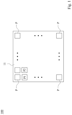
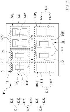
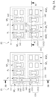
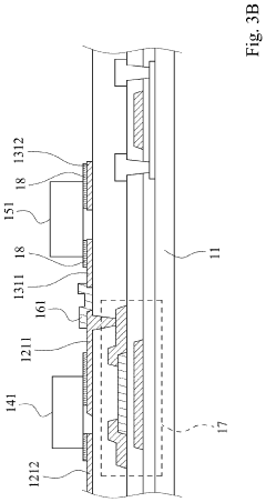
Redundant pixel architecture in ILED displays
PatentActiveUS10679911B2
Innovation
- The method involves creating sub-pixel assemblies with primary micro-LEDs, identifying and replacing defective micro-LEDs, and physically severing current paths to integrate additional replacement micro-LEDs, allowing for the creation of repaired sub-pixel assemblies with two defective and one operable micro-LEDs connected to separate branches of a current path, enhancing manufacturing efficiency and reducing power consumption.
Selectable-repairing micro light emitting diode display and repairing method thereof
PatentActiveUS11843074B2
Innovation
- A selectable-repairing Micro LED display with a backplane, pixel units, and micro light emitting elements, where each pixel unit includes original sub-pixel units and selectable-repairing sub-pixel units with separate pads, allowing for flexible repair by transferring and bonding micro light emitting elements to compensation areas and forming repairing circuits between original and repairing pads.
Yield Improvement Strategies for MicroLED Manufacturing
Yield improvement remains a critical challenge in MicroLED manufacturing, with defect rates significantly impacting production costs and commercial viability. Redundancy pixel mapping and rework flows represent essential strategies for improving overall manufacturing yield by addressing inevitable defects that occur during the complex fabrication process.
The implementation of redundancy systems begins with comprehensive pixel mapping techniques that identify and categorize defective pixels across display panels. Advanced imaging systems utilizing high-resolution cameras and specialized algorithms can detect various defect types including dead pixels, color variations, and brightness inconsistencies. This mapping process creates a detailed defect database that serves as the foundation for subsequent repair strategies.
Once defective pixels are identified, redundancy architectures provide alternative pathways to maintain display functionality. These architectures typically incorporate spare pixels or redundant driving circuits that can be activated when primary pixels fail. The redundancy ratio—the number of spare pixels relative to active pixels—must be carefully optimized to balance yield improvement against increased manufacturing complexity and cost.
Rework flows represent the procedural framework for implementing repairs based on pixel mapping data. These workflows typically follow a hierarchical approach, beginning with software-based corrections for minor defects such as brightness variations. For more severe defects, physical rework processes may be employed, including laser repair techniques, micro-soldering, or complete pixel replacement depending on the defect type and severity.
The integration of automated decision systems has significantly enhanced rework efficiency. These systems analyze defect patterns and automatically determine the most appropriate repair strategy based on predefined parameters such as defect type, location, and density. Machine learning algorithms continuously improve these decision processes by analyzing repair outcomes and refining selection criteria.
Real-time monitoring systems play a crucial role in tracking repair effectiveness and preventing cascading failures. These systems provide immediate feedback on repair quality and can trigger additional interventions when necessary. The data collected through these monitoring systems also contributes to continuous process improvement by identifying recurring defect patterns and their root causes.
The economic viability of redundancy and rework strategies depends heavily on balancing repair costs against yield improvements. Cost modeling tools help manufacturers determine optimal intervention points where repair remains more economical than scrapping. As MicroLED technology matures, these yield improvement strategies will continue to evolve, potentially incorporating more advanced techniques such as self-healing materials and adaptive redundancy systems.
Cost-Benefit Analysis of Redundancy Implementation
Implementing redundancy in MicroLED displays represents a significant investment decision that requires thorough cost-benefit analysis. The financial implications of redundancy pixel mapping must be evaluated against the potential savings in repair costs and yield improvements. Initial implementation costs include additional design complexity, increased silicon area for redundant pixels, and more sophisticated control circuitry.
Manufacturing expenses also rise due to the need for more complex pixel addressing schemes and additional testing procedures. However, these upfront investments must be weighed against the substantial benefits in production yield. Statistical analysis indicates that strategic redundancy implementation can improve final display yield by 15-30%, depending on the native defect density of the MicroLED manufacturing process.
The economic equation becomes particularly favorable when considering high-value applications such as AR/VR headsets, premium televisions, and automotive displays. In these segments, the cost of scrapping defective panels significantly outweighs the incremental cost of implementing redundancy. For example, in automotive displays where reliability requirements are stringent, the redundancy implementation cost typically represents only 7-12% of the potential loss from defective units.
Operational benefits extend beyond direct manufacturing costs. Redundancy systems enable more efficient repair workflows, reducing the time and resources required for rework processes. This translates to approximately 25-40% reduction in repair cycle time and associated labor costs. Additionally, the ability to address pixel failures in the field through redundancy activation provides significant warranty cost reductions and enhanced customer satisfaction.
The return on investment timeline varies by application and production volume. For high-volume consumer electronics, ROI typically materializes within 6-18 months of implementation. Premium display applications with lower volumes but higher margins may see positive returns even sooner, often within a single production cycle.
Long-term strategic benefits include improved manufacturing flexibility, enhanced product reliability, and the ability to maintain higher quality standards. These factors contribute to brand value and market positioning that extend beyond direct cost calculations. Companies implementing robust redundancy strategies have demonstrated 20-35% lower warranty claim rates compared to competitors using traditional repair-only approaches.
Unlock deeper insights with Patsnap Eureka Quick Research — get a full tech report to explore trends and direct your research. Try now!
Generate Your Research Report Instantly with AI Agent
Supercharge your innovation with Patsnap Eureka AI Agent Platform!