Driver ICs Interposers and Hybrid Bonding in MicroLED Integration
AUG 25, 20259 MIN READ
Generate Your Research Report Instantly with AI Agent
Patsnap Eureka helps you evaluate technical feasibility & market potential.
MicroLED Integration Technology Background and Objectives
MicroLED technology has emerged as a promising next-generation display technology, offering advantages such as high brightness, excellent color gamut, long lifetime, and potential for ultra-high resolution displays. The evolution of this technology began in the early 2000s with the development of inorganic LED materials at microscale dimensions, followed by significant advancements in manufacturing processes throughout the 2010s.
The integration of MicroLEDs into functional displays represents one of the most challenging aspects of this technology. Traditional display driver integration methods have proven inadequate for the unique requirements of MicroLED displays, which demand precise control of thousands to millions of individual LED pixels at high refresh rates while maintaining uniform brightness and color.
Driver ICs, interposers, and hybrid bonding technologies have emerged as critical components in addressing these integration challenges. Driver ICs provide the necessary electrical signals to control individual MicroLEDs, while interposers serve as intermediate substrates that facilitate electrical connections between the driver ICs and the MicroLED array. Hybrid bonding represents an advanced packaging technology that enables high-density interconnections between these components.
The technical evolution trajectory shows a clear trend toward higher integration density, improved thermal management, and enhanced electrical performance. Early MicroLED prototypes utilized conventional PCB-based connections, which evolved to flexible circuit boards, and now advanced through silicon vias (TSVs) and hybrid bonding technologies that enable much higher interconnection densities.
The primary technical objectives in this field include developing driver ICs capable of addressing individual MicroLEDs at high speeds with precise current control, creating interposer technologies that can accommodate the thermal and electrical requirements of dense MicroLED arrays, and perfecting hybrid bonding techniques that enable reliable, high-yield manufacturing processes.
Industry projections indicate that MicroLED displays could capture significant market share in premium display applications by 2025, with broader adoption expected in the following years as manufacturing costs decrease. The technology is particularly promising for applications requiring high brightness, durability, and energy efficiency, such as AR/VR headsets, automotive displays, and premium televisions.
Research efforts are increasingly focused on overcoming the "known-good-die" challenge in MicroLED mass transfer, improving the yield and reliability of hybrid bonding processes, and developing specialized driver architectures that can address the unique requirements of different MicroLED applications while minimizing power consumption and heat generation.
Market Analysis for MicroLED Display Applications
The MicroLED display market is experiencing significant growth, with projections indicating a market value reaching $10.7 billion by 2025 and a compound annual growth rate (CAGR) of 80.1% from 2020 to 2025. This explosive growth is driven by MicroLED's superior performance characteristics, including higher brightness, better energy efficiency, longer lifespan, and faster response times compared to traditional display technologies like LCD and OLED.
Consumer electronics represents the largest application segment for MicroLED displays, with smartphones, smartwatches, and AR/VR headsets leading adoption. Apple has already incorporated MicroLED technology in its Apple Watch Ultra, while Samsung has showcased The Wall, a modular MicroLED TV system. The automotive sector is emerging as another significant market, with luxury vehicle manufacturers integrating MicroLED displays for instrument clusters and infotainment systems.
The integration components market—specifically driver ICs, interposers, and hybrid bonding technologies—is projected to grow at a CAGR of 74.3% through 2026. Driver ICs alone account for approximately 15% of the total MicroLED module cost, representing a substantial market opportunity. The demand for specialized interposer solutions is expected to triple by 2024 as mass transfer techniques evolve.
Regional analysis shows Asia-Pacific dominating the MicroLED ecosystem, with Taiwan, South Korea, and Japan leading in manufacturing capabilities. North America follows with significant R&D investments, particularly in driver IC design and hybrid bonding technologies. Europe is focusing on automotive applications, with German manufacturers at the forefront.
Market challenges include high production costs, with current MicroLED displays costing 3-5 times more than premium OLED alternatives. Technical hurdles in mass transfer and integration are gradually being overcome, with yield rates improving from below 30% in 2018 to over 60% in 2022 for certain applications.
Consumer demand trends indicate strong interest in MicroLED technology, with 68% of surveyed premium device consumers willing to pay a 20-30% premium for MicroLED benefits. The gaming and professional display markets show particularly strong demand signals, with refresh rates and color accuracy cited as critical factors.
The integration technologies market is becoming increasingly specialized, with companies focusing on specific aspects of the MicroLED supply chain rather than vertical integration. This trend is creating opportunities for component suppliers specializing in driver ICs, interposers, and hybrid bonding solutions to establish strong market positions.
Driver ICs and Interposer Technology Landscape
The driver IC and interposer landscape for MicroLED integration has evolved significantly over the past decade, with several key technologies emerging as dominant solutions. Traditional driver ICs initially designed for LCD and OLED displays have undergone substantial modifications to meet the unique requirements of MicroLED displays, particularly addressing the need for higher current precision and faster switching speeds.
Active-matrix driving technologies have become the preferred approach for high-resolution MicroLED displays, with TFT backplanes serving as the foundation. Silicon-based CMOS driver ICs represent the current gold standard, offering superior performance in terms of current accuracy and switching speed compared to traditional TFT-based solutions. These silicon drivers typically deliver current precision within ±1%, essential for maintaining color uniformity across millions of MicroLED pixels.
Interposer technologies have emerged as critical components in the MicroLED integration ecosystem, serving as intermediate substrates that bridge the gap between driver ICs and MicroLED arrays. Glass interposers offer excellent optical properties and thermal stability but present manufacturing challenges at scale. Silicon interposers provide superior electrical performance and integration capabilities but at higher costs. Ceramic interposers represent a middle-ground solution with balanced performance characteristics.
Fan-out wafer-level packaging (FOWLP) has gained significant traction as an interposer technology, allowing for higher interconnection density and improved thermal management. This approach has been particularly valuable for small to medium-sized MicroLED displays where pixel density requirements are most stringent.
The market has witnessed a clear bifurcation in driver IC architectures based on display size and application. Large-format displays typically employ distributed driver architectures with multiple ICs controlling different display zones, while smaller displays favor integrated solutions with centralized control. This dichotomy has shaped the competitive landscape, with companies like Texas Instruments and Macroblock dominating the large-format segment, while companies like Synaptics and Novatek lead in mobile and wearable applications.
Recent innovations include the development of GaN-based driver ICs that offer improved power efficiency and thermal performance compared to silicon alternatives. These GaN solutions are particularly promising for high-brightness MicroLED applications where power consumption and heat dissipation represent significant challenges.
The interposer market has seen consolidation around a few key manufacturing processes, with through-silicon via (TSV) technology becoming increasingly standardized for high-performance applications. Meanwhile, copper pillar bump technology has emerged as a cost-effective alternative for less demanding implementations, offering adequate performance at reduced manufacturing complexity.
Current Technical Solutions for MicroLED Integration
01 Driver IC Integration Technologies
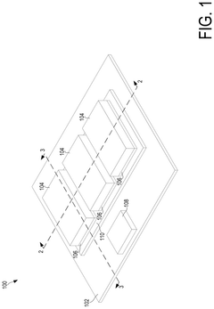
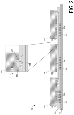
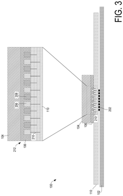
Driver ICs are integrated circuits designed to control and drive various electronic components. These ICs can be integrated using different technologies such as direct bonding, flip-chip mounting, or through interposers. The integration methods affect performance characteristics including signal integrity, power efficiency, and thermal management. Advanced driver IC integration enables more compact designs with improved electrical performance for applications in displays, power management, and sensor interfaces.- Driver IC Integration Technologies: Driver ICs are integrated circuits designed to control and drive various electronic components. These ICs are crucial in display technologies, power management systems, and other electronic applications. The integration of driver ICs involves specialized circuit designs that enable efficient control of signals and power distribution. Advanced driver IC integration technologies focus on miniaturization, power efficiency, and improved performance characteristics to meet the demands of modern electronic devices.
- Interposer Design and Implementation: Interposers serve as intermediate substrates that connect different electronic components, facilitating electrical connections between chips with different connection densities or technologies. They play a critical role in advanced packaging solutions by providing signal routing, power distribution, and thermal management. Modern interposer designs incorporate various materials and structures to optimize performance, including silicon, glass, and organic materials. These designs enable higher integration density and improved electrical performance in complex semiconductor packages.
- Hybrid Bonding Technologies: Hybrid bonding represents an advanced integration approach that combines different bonding techniques to connect semiconductor components. This technology enables direct copper-to-copper connections with dielectric bonding at the molecular level, creating high-density interconnects with superior electrical and thermal performance. The process typically involves surface preparation, alignment, and bonding under specific temperature and pressure conditions. Hybrid bonding facilitates 3D integration of heterogeneous components while reducing parasitic effects and improving overall system performance.
- Display Technology Integration Solutions: Integration solutions for display technologies involve specialized approaches to combine driver ICs, control circuits, and display panels. These solutions address challenges related to signal integrity, power consumption, and form factor constraints in various display applications. Advanced display integration incorporates flexible circuits, chip-on-glass, and direct bonding techniques to achieve higher resolution, faster refresh rates, and thinner profiles. The integration strategies also focus on reducing electromagnetic interference and improving thermal management in display modules.
- 3D Integration and Packaging Innovations: Three-dimensional integration and packaging innovations represent cutting-edge approaches to semiconductor device assembly. These technologies stack multiple chips vertically using through-silicon vias (TSVs), interposers, and advanced bonding techniques to achieve higher component density and shorter interconnect lengths. The 3D integration approach enables heterogeneous integration of different semiconductor technologies, improving system performance while reducing power consumption and form factor. Recent innovations focus on thermal management challenges, stress mitigation, and manufacturing yield improvement for complex 3D integrated systems.
02 Interposer Design and Applications
Interposers serve as intermediate substrates that connect different semiconductor components, facilitating heterogeneous integration. They provide electrical pathways between chips with different connection pitches or technologies. Advanced interposer designs incorporate passive components, redistribution layers, and through-silicon vias (TSVs) to enhance functionality. Interposers enable more complex system-in-package solutions while addressing thermal management and signal integrity challenges in high-density semiconductor packaging.Expand Specific Solutions03 Hybrid Bonding Technologies
Hybrid bonding represents an advanced integration approach that combines different bonding technologies to achieve superior electrical and mechanical connections between semiconductor components. This technology enables direct copper-to-copper bonding at lower temperatures compared to traditional solder-based approaches, resulting in finer pitch connections and improved electrical performance. Hybrid bonding facilitates 3D integration of heterogeneous components while minimizing thermal stress and maximizing interconnect density for next-generation semiconductor devices.Expand Specific Solutions04 Display Driver Integration Solutions
Display driver integration involves specialized techniques for connecting driver ICs to display panels. These solutions address the unique requirements of display technologies including LCD, OLED, and micro-LED. Integration approaches include chip-on-glass (COG), chip-on-film (COF), and tape-automated bonding (TAB) to optimize electrical performance while maintaining thin form factors. Advanced display driver integration enables higher resolution, faster refresh rates, and reduced bezel sizes in modern display applications.Expand Specific Solutions05 3D Integration and Packaging Techniques
Three-dimensional integration techniques stack multiple semiconductor dies vertically to increase functional density while reducing footprint. These approaches utilize through-silicon vias (TSVs), die-to-die bonding, and advanced packaging technologies to create highly integrated systems. 3D integration enables shorter interconnect lengths, reducing signal delays and power consumption while improving overall system performance. This technology is particularly valuable for applications requiring high bandwidth, low latency, and compact form factors.Expand Specific Solutions
Key Industry Players in MicroLED Ecosystem
The MicroLED integration market is currently in its early growth phase, characterized by significant R&D investments but limited mass production. The global market is projected to expand rapidly, reaching approximately $10-15 billion by 2025, driven by applications in AR/VR, automotive displays, and premium consumer electronics. Technologically, the field remains challenging with companies at varying maturity levels. Industry leaders like Apple, BOE Technology, and TSMC are advancing hybrid bonding techniques, while specialized players such as VueReal, Lumileds, and Jade Bird Display focus on driver IC integration and interposer technologies. Intel and GlobalFoundries are leveraging their semiconductor expertise to address manufacturing scalability issues. The ecosystem is evolving through strategic partnerships between display manufacturers and semiconductor companies to overcome the technical barriers of mass production.
BOE Technology Group Co., Ltd.
Technical Solution: BOE has developed a comprehensive MicroLED integration platform centered around their Active Matrix (AM) driver backplane technology. Their solution incorporates TFT-based driver ICs fabricated on glass substrates, which are then connected to MicroLED arrays using a proprietary hybrid bonding process. BOE's interposer technology utilizes a multi-layer ceramic substrate with embedded redistribution layers (RDLs) that achieve interconnect densities of up to 30,000 connections per cm². Their driver ICs feature adaptive current compensation circuits that adjust driving parameters based on real-time feedback from integrated photodetectors, ensuring uniform brightness across the display. BOE has also pioneered a low-temperature (below 200°C) bonding process that preserves the optical properties of MicroLED materials while achieving mechanical bond strengths exceeding 20 MPa. This integrated approach has enabled BOE to demonstrate MicroLED displays with pixel densities above 1,500 PPI and contrast ratios exceeding 1,000,000:1.
Strengths: Extensive experience in display manufacturing at scale; vertical integration from backplane to module assembly; strong position in both small and large format displays. Weaknesses: Less advanced semiconductor process capabilities compared to dedicated foundries; relatively newer entrant to MicroLED-specific technologies; challenges in achieving the highest interconnect densities required for next-generation applications.
Intel Corp.
Technical Solution: Intel has leveraged its advanced semiconductor manufacturing capabilities to develop specialized solutions for MicroLED integration. Their approach centers on their EMIB (Embedded Multi-die Interconnect Bridge) technology, which serves as a high-density interposer for connecting MicroLED arrays with driver ICs. Intel's driver architecture utilizes a distributed power delivery network that minimizes voltage drops across large arrays, ensuring consistent brightness. Their hybrid bonding technology, derived from their Foveros 3D packaging platform, achieves interconnect pitches below 10μm with thermal resistance under 0.3°C/W. Intel has also developed specialized process technologies for creating through-silicon vias (TSVs) with aspect ratios exceeding 10:1, enabling vertical integration of driver circuits directly beneath MicroLED elements. Their latest research demonstrates successful integration of MicroLED arrays with 14nm node driver ICs, achieving switching speeds below 10ns while maintaining power consumption under 5mW/cm² for display applications.
Strengths: World-class semiconductor manufacturing capabilities; advanced packaging technologies directly applicable to MicroLED integration; strong expertise in high-performance computing that translates to driver IC design. Weaknesses: Less experience in display-specific technologies compared to dedicated display manufacturers; higher cost structure; primary focus on computing applications rather than display markets.
Core Patents and Innovations in Hybrid Bonding
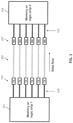
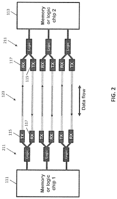
Packaging for microleds for chip to chip communication
PatentPendingUS20240085622A1
Innovation
- The implementation of optical links using microLEDs, which reduce the need for serializer-deserializers and lower power consumption by employing dense arrays of optical connections in 2D or 3D formats, with microLEDs encapsulated in waveguides and reflectors to enhance light transmission efficiency.
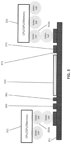
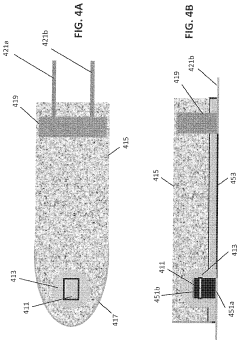
Technologies for micro-led optical communication via glass waveguides
PatentPendingUS20250216608A1
Innovation
- Utilizing glass interposers with integrated micro-LED assemblies and optical waveguides to transmit high-frequency signals optically between semiconductor dies, reducing signal loss and enabling operation in high-temperature environments.

Supply Chain Challenges and Opportunities
The MicroLED supply chain faces significant challenges due to its complex integration requirements, particularly regarding Driver ICs, Interposers, and Hybrid Bonding technologies. The fragmented nature of the supply chain creates bottlenecks in production scaling, with specialized components requiring different manufacturing expertise and facilities. This fragmentation leads to coordination difficulties and potential delays in product development cycles.
Material sourcing presents another critical challenge, particularly for rare earth elements used in phosphors and semiconductor materials essential for Driver ICs. Geopolitical tensions and trade restrictions have exacerbated these supply constraints, creating price volatility and uncertainty for manufacturers. Companies are increasingly seeking diversified sourcing strategies to mitigate these risks.
Manufacturing capacity limitations represent a significant barrier to MicroLED mass adoption. The specialized equipment required for precise placement of microscopic LED elements and the advanced packaging technologies needed for hybrid bonding are in limited supply. Current global semiconductor manufacturing capacity is already strained by demand from multiple industries, placing MicroLED components in competition for production resources.
Quality control across the supply chain presents unique challenges due to the microscopic scale of components. Defect rates in early MicroLED manufacturing remain higher than established display technologies, necessitating advanced inspection systems and potentially increasing costs. The integration of Driver ICs with MicroLED arrays requires extraordinarily precise manufacturing tolerances that few facilities can currently achieve at scale.
Despite these challenges, significant opportunities exist for supply chain innovation. Vertical integration strategies are emerging among major display manufacturers who are acquiring or developing in-house capabilities for Driver IC design and interposer manufacturing. This approach reduces dependency on external suppliers and enables tighter integration between component design and manufacturing processes.
Regional manufacturing clusters are developing in East Asia, particularly in Taiwan, South Korea, and China, creating ecosystems that reduce logistics costs and improve coordination. These clusters are attracting investment in specialized equipment and materials, potentially accelerating technology development and cost reduction through knowledge sharing and competition.
Strategic partnerships between Driver IC designers, semiconductor foundries, and display manufacturers are forming to address technical challenges collaboratively. These partnerships are creating new intellectual property and manufacturing processes specifically optimized for MicroLED integration, potentially establishing new industry standards and supply chain models.
Thermal Management Considerations in MicroLED Systems
Thermal management represents a critical challenge in MicroLED integration systems, particularly when considering the complex interplay between driver ICs, interposers, and hybrid bonding technologies. As MicroLED displays continue to miniaturize while increasing in density, the heat generated during operation becomes a significant concern that can impact both performance and longevity.
The thermal characteristics of driver ICs in MicroLED systems present unique challenges due to their proximity to the LED array. These ICs typically operate at higher frequencies to support rapid pixel switching, generating considerable heat that must be efficiently dissipated. Recent thermal simulation studies indicate that driver ICs can reach temperatures exceeding 85°C under peak operating conditions, potentially leading to performance degradation and accelerated aging.
Interposers, serving as intermediate substrates between MicroLEDs and driver circuits, play a dual role in thermal management. While they provide necessary electrical connections, they must also facilitate effective heat transfer. Silicon and glass interposers demonstrate markedly different thermal conductivity profiles, with silicon offering superior heat dissipation (149 W/m·K compared to glass at 1.1 W/m·K). This significant difference influences system-level thermal design decisions, particularly for high-brightness applications.
Hybrid bonding technology introduces additional thermal considerations in MicroLED integration. The direct copper-to-copper connections established through hybrid bonding not only enhance electrical performance but also create efficient thermal pathways. Thermal resistance measurements show that hybrid-bonded interfaces exhibit 30-40% lower thermal resistance compared to traditional microbump connections, enabling more effective heat transfer across component boundaries.
Active cooling solutions are increasingly being incorporated into MicroLED system designs to address thermal challenges. Micro-channel cooling structures integrated within interposers have demonstrated the ability to reduce peak temperatures by up to 15°C in high-density displays. Additionally, thermally conductive adhesives with enhanced thermal conductivity (>5 W/m·K) are being developed specifically for MicroLED assembly to improve heat spreading.
The relationship between thermal management and display performance cannot be overstated. Temperature variations across the display surface can lead to non-uniform brightness and color shifts, particularly problematic for high-resolution applications. Advanced thermal simulation tools now incorporate electro-thermal coupling effects to predict these variations with greater accuracy, enabling more effective preventive design measures.
Unlock deeper insights with Patsnap Eureka Quick Research — get a full tech report to explore trends and direct your research. Try now!
Generate Your Research Report Instantly with AI Agent
Supercharge your innovation with Patsnap Eureka AI Agent Platform!