Roadmap from Pilot Production to High Volume MicroLED Manufacturing
AUG 25, 20259 MIN READ
Generate Your Research Report Instantly with AI Agent
Patsnap Eureka helps you evaluate technical feasibility & market potential.
MicroLED Manufacturing Evolution and Objectives
MicroLED technology has evolved significantly since its inception in the early 2000s, transitioning from laboratory experiments to pilot production lines. The journey began with fundamental research on inorganic LED materials and their potential application in display technologies. Early developments focused on overcoming basic technical challenges such as pixel formation and light emission efficiency, with limited production capabilities restricted to small-scale laboratory environments.
The mid-2010s marked a pivotal shift as major technology companies began acquiring MicroLED startups, signaling industry recognition of the technology's potential. This period saw the establishment of the first pilot production facilities, characterized by semi-automated processes with significant manual intervention and relatively low yields. These pilot lines typically produced small quantities of specialized displays for premium applications, demonstrating the technology's capabilities while highlighting the challenges of scaling production.
Current MicroLED manufacturing stands at a critical juncture between pilot production and high-volume manufacturing. The industry faces the challenge of transitioning from batch processing with moderate yields to continuous production flows with consistently high yields necessary for mass market adoption. This evolution requires significant advancements in automation, process control, and quality assurance systems.
The primary objective of MicroLED manufacturing evolution is to establish economically viable high-volume production capabilities that can compete with established display technologies like OLED and LCD. This requires achieving several key technical milestones: reducing defect rates to below 1 part per million, increasing transfer yields to over 99.9%, and developing fully automated production lines capable of handling millions of microscopic LED elements with precision and reliability.
Secondary objectives include reducing manufacturing costs through economies of scale and process optimization, shortening production cycle times, and developing flexible manufacturing systems capable of producing various display sizes and configurations without major retooling. These improvements aim to position MicroLED as a mainstream display technology rather than a niche premium offering.
The roadmap toward high-volume manufacturing must address several critical challenges, including mass transfer techniques for efficiently placing millions of tiny LED elements, developing inspection and repair systems capable of identifying and correcting defects at unprecedented scales, and creating integrated supply chains for specialized materials and components. Success in these areas will determine whether MicroLED can fulfill its promise as the next generation of display technology.
Market Demand Analysis for MicroLED Displays
The MicroLED display market is experiencing significant growth potential driven by several key factors. Consumer electronics manufacturers are increasingly seeking advanced display technologies that offer superior brightness, energy efficiency, and color accuracy. MicroLED displays, with their self-emissive pixels and absence of backlighting requirements, deliver exceptional contrast ratios and power efficiency that exceed both LCD and OLED technologies. This positions them as the next evolutionary step in display technology.
Market research indicates that the global MicroLED market is projected to grow substantially over the next decade, with particularly strong demand emerging in premium segments. The automotive industry represents a significant growth vector, as vehicle manufacturers integrate more sophisticated display systems into dashboards and entertainment consoles. The inherent durability and brightness of MicroLED technology make it especially suitable for automotive applications where displays must function reliably under varying light conditions.
The wearable technology sector presents another substantial market opportunity. Smartwatch manufacturers are exploring MicroLED implementation due to its superior power efficiency, which directly addresses battery life limitations in compact devices. Additionally, the augmented reality (AR) and virtual reality (VR) segments show promising demand forecasts, as these applications benefit from MicroLED's high brightness, low latency, and compact form factor.
Premium television and professional display markets are demonstrating early adoption patterns. High-end consumers and commercial users are willing to pay premium prices for the superior visual experience offered by MicroLED displays. This segment is expected to drive initial market growth while manufacturing processes mature and costs decrease.
Regional analysis reveals that East Asian markets, particularly South Korea, Japan, and Taiwan, show the strongest immediate demand due to their established electronics manufacturing ecosystems. North American and European markets follow closely, primarily driven by premium consumer segments and professional applications.
The transition from pilot to high-volume manufacturing is being accelerated by increasing consumer expectations for display quality. As smartphone and television manufacturers compete on display specifications, the pressure to commercialize advanced technologies like MicroLED intensifies. This competitive landscape is creating market pull that encourages investment in manufacturing scale-up.
Despite strong demand signals, price sensitivity remains a critical factor. Current manufacturing costs position MicroLED displays at premium price points, limiting mass-market penetration. However, industry forecasts suggest that as production volumes increase and manufacturing processes mature, price points will decrease sufficiently to address broader market segments within the next 3-5 years.
Technical Barriers in MicroLED Mass Production
Despite significant advancements in MicroLED technology, mass production remains hindered by several critical technical barriers. The miniaturization of LED chips to microscale dimensions introduces unprecedented manufacturing challenges that conventional LED production techniques cannot adequately address.
Mass transfer represents perhaps the most formidable obstacle in MicroLED manufacturing. Current technologies struggle to achieve the necessary precision, speed, and yield when transferring millions of tiny MicroLED chips from growth substrates to display backplanes. Pick-and-place methods, while precise, are prohibitively slow for high-volume production, whereas stamp transfer techniques face challenges with consistent yield across large areas.
Defect management presents another significant hurdle. The microscopic size of MicroLED chips magnifies the impact of even minor defects, with a single defective pixel potentially compromising an entire display. Current inspection and repair technologies cannot efficiently identify and address these defects at production speeds required for commercial viability.
Color conversion and uniformity control pose substantial technical difficulties. Achieving consistent performance across millions of individual MicroLED elements requires unprecedented precision in manufacturing. Variations in chip size, epitaxial quality, or transfer process can result in visible non-uniformities in brightness and color, significantly impacting display quality.
Interconnection and integration challenges further complicate production scaling. The electrical connection of millions of microscopic elements demands novel approaches to circuit design and manufacturing. Traditional bonding techniques prove inadequate at the microscale, necessitating innovations in interconnection technology.
Substrate and backplane compatibility issues create additional complexity. The integration of MicroLED elements with driving circuitry requires precise alignment and electrical connectivity across different material systems, presenting significant thermal and mechanical challenges during manufacturing.
Testing and quality assurance methodologies suitable for high-volume production remain underdeveloped. Current testing approaches are too time-consuming for production environments, yet comprehensive testing is essential given the high precision requirements of MicroLED displays.
Cost-effective manufacturing equipment specifically designed for MicroLED production represents a critical gap in the industry. Existing semiconductor and display manufacturing tools require substantial modification to address the unique requirements of MicroLED fabrication, creating significant capital investment barriers for manufacturers entering this space.
Current Production Scaling Solutions
01 Mass production techniques for MicroLED displays
Various manufacturing techniques have been developed to enable mass production of MicroLED displays. These include advanced transfer processes, automated assembly lines, and specialized equipment designed to handle the miniature LED components efficiently. These techniques aim to increase throughput while maintaining precision in the placement and connection of microLEDs, which is crucial for achieving high-volume manufacturing capabilities.- Mass production techniques for MicroLED displays: Various techniques have been developed to enable mass production of MicroLED displays, including automated assembly processes, transfer printing methods, and integration with existing manufacturing infrastructure. These approaches aim to increase throughput and yield while reducing production costs, making MicroLED technology more commercially viable for large-scale manufacturing.
- Transfer and bonding processes for high-volume manufacturing: Efficient transfer and bonding processes are critical for high-volume MicroLED manufacturing. These include mass transfer techniques that can simultaneously place multiple MicroLED chips onto substrates, advanced bonding methods that ensure reliable electrical connections, and pick-and-place technologies optimized for microscale devices. These processes help overcome one of the major bottlenecks in MicroLED production.
- Defect inspection and repair strategies for volume production: To maintain high yields in volume manufacturing, advanced defect inspection and repair strategies have been developed. These include automated optical inspection systems, electrical testing methodologies, and repair techniques that can identify and address defective pixels. Such approaches are essential for ensuring quality control in mass production environments.
- Equipment and tooling for scaled manufacturing: Specialized equipment and tooling have been designed to support high-volume MicroLED manufacturing. This includes custom handling systems for fragile microchips, precision alignment tools, specialized deposition equipment, and automated testing platforms. These tools enable manufacturers to scale production while maintaining the precision required for MicroLED fabrication.
- Integration of MicroLED manufacturing with existing display production lines: Methods for integrating MicroLED manufacturing processes with existing display production infrastructure have been developed to leverage current investments and expertise. These approaches include compatible process steps, modular manufacturing systems, and hybrid production techniques that can be implemented in conventional display fabrication facilities, enabling a smoother transition to MicroLED technology at volume.
02 Substrate and wafer processing for high-volume production
Specialized substrate and wafer processing methods have been developed to support high-volume MicroLED manufacturing. These include techniques for growing LED epitaxial layers on large wafers, methods for wafer bonding, and processes for substrate removal or transfer. These approaches enable parallel processing of thousands of MicroLED units simultaneously, significantly increasing production volume while reducing costs.Expand Specific Solutions03 Automated inspection and repair systems
To maintain high yields in volume manufacturing, automated inspection and repair systems have been developed specifically for MicroLED production. These systems use machine vision and precision robotics to identify defective pixels or connections and either repair or replace them during the manufacturing process. This capability is essential for achieving economically viable production volumes by minimizing waste and maximizing functional display yield.Expand Specific Solutions04 Scalable bonding and interconnection technologies
Novel bonding and interconnection technologies have been developed to address the challenges of connecting millions of tiny MicroLEDs to driving circuits in a scalable manner. These include flip-chip bonding, mass transfer techniques, and innovative interconnect architectures that can be implemented in high-volume manufacturing environments. These technologies enable reliable electrical and mechanical connections while maintaining the production throughput needed for commercial viability.Expand Specific Solutions05 Equipment and facility design for volume manufacturing
Specialized equipment and manufacturing facility designs have been created specifically for high-volume MicroLED production. These include custom handling systems, environmental control measures, and factory automation solutions that address the unique challenges of working with microscopic LED components at scale. The equipment is designed to maximize throughput while maintaining the precision required for MicroLED assembly, enabling manufacturers to achieve the production volumes needed for commercial applications.Expand Specific Solutions
Key Industry Players in MicroLED Manufacturing
The MicroLED manufacturing landscape is transitioning from pilot production to high-volume manufacturing, currently in the early growth phase with market projections showing significant expansion potential. While technical maturity remains moderate, key players are making substantial advancements. Samsung Electronics and BOE Technology lead with established manufacturing capabilities, while LG Electronics and TCL China Star are rapidly scaling their production lines. Companies like eLux and Lumileds are developing innovative transfer technologies, with Goertek and Huawei focusing on integration solutions. Asian manufacturers, particularly from China and South Korea, dominate the competitive landscape, with specialized equipment providers like 3D-Micromac supporting the ecosystem's development toward cost-effective mass production.
BOE Technology Group Co., Ltd.
Technical Solution: BOE has established a comprehensive MicroLED manufacturing roadmap centered on progressive scaling through modular production systems. Their approach begins with semi-automated pilot lines focused on specialized applications, followed by incremental expansion using standardized production modules that can be replicated to increase capacity. BOE's technology incorporates a multi-stage transfer process that combines wafer-level processing with panel-level assembly to optimize both precision and throughput[5]. They've developed specialized handling systems for ultra-small MicroLED chips that maintain positional accuracy while increasing transfer speeds. BOE's scaling strategy emphasizes yield improvement through advanced defect detection systems using AI-powered optical inspection that can identify potential failures before final assembly. Their manufacturing roadmap includes proprietary repair technologies that can address defective pixels post-transfer, significantly improving economic viability in early production phases[6]. BOE has also invested in specialized equipment for high-precision bonding that maintains electrical and optical performance at mass production speeds.
Strengths: Strong integration with existing display manufacturing infrastructure; advanced defect management and repair technologies that improve production economics; scalable modular production approach that allows gradual capacity expansion. Weaknesses: Mass transfer technology still faces consistency challenges at highest volume production; current processes have higher material waste compared to competitors; technology optimization still ongoing for smallest MicroLED form factors.
Samsung Electronics Co., Ltd.
Technical Solution: Samsung has developed a comprehensive roadmap for MicroLED manufacturing transition from pilot to high volume production. Their approach centers on a modular production system that allows gradual scaling of capacity. Samsung's technology involves a mass transfer process using elastomer stamps that can pick up and place thousands of MicroLED chips simultaneously[1]. They've implemented a three-phase scaling strategy: initial low-volume production using semi-automated lines for premium products (The Wall), mid-scale production with increased automation and improved yield management systems, and finally full-scale manufacturing with custom-designed equipment and fully integrated production lines. Samsung has invested in proprietary inspection and repair technologies that identify defective LEDs before final assembly, significantly improving yields in mass production scenarios[2]. Their manufacturing roadmap includes specialized equipment for handling sub-10μm MicroLED chips and advanced bonding techniques that maintain placement accuracy at high throughput rates.
Strengths: Industry-leading mass transfer technology with proven capability to handle ultra-small MicroLED chips; extensive experience in display manufacturing that facilitates scaling; strong vertical integration from chip fabrication to final assembly. Weaknesses: High capital expenditure requirements for full-scale implementation; current processes still face yield challenges at consumer electronics price points; technology primarily optimized for larger display applications rather than smaller form factors.
Critical Patents and Innovations in MicroLED Manufacturing
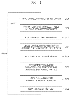
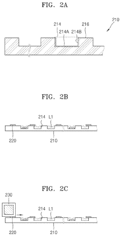
Method of manufacturing micro-led display
PatentActiveUS20220190192A1
Innovation
- A method involving fluidic self-assembly (FSA) using a penetrating solvent that is vaporized by radiating light, allowing for the transfer of micro LEDs from an interposer to a driving substrate, combined with recycling techniques and alignment markers, enables efficient and scalable manufacturing of large-size micro LED displays.
Method of manufacturing micro light-emitting diode
PatentActiveJP2024026189A
Innovation
- The micro-LED device incorporates a sidewall current limiting region with specific dimensions and conductivity characteristics, along with additional current limiting regions, to enhance luminous efficiency and uniformity of current distribution.
Supply Chain Optimization Strategies
The transition from pilot production to high-volume manufacturing of MicroLED displays necessitates robust supply chain optimization strategies. Current MicroLED supply chains face significant fragmentation, with specialized components sourced from diverse global suppliers, creating vulnerabilities in production continuity. Establishing strategic partnerships with key component manufacturers, particularly for specialized materials like quantum dot films and epitaxial wafers, can secure priority access during industry-wide shortages.
Vertical integration represents a critical optimization approach, with leading manufacturers increasingly acquiring suppliers of critical components to maintain quality control and reduce dependency on external vendors. This strategy has proven particularly effective for companies like Samsung and Apple, who have invested in controlling their LED chip production capabilities to ensure consistent supply for their display manufacturing operations.
Just-in-time inventory management systems, when adapted specifically for MicroLED production requirements, can significantly reduce warehousing costs while maintaining production efficiency. However, these systems must be balanced with strategic stockpiling of critical components that face frequent supply constraints or have extended lead times, particularly specialized semiconductor materials and custom optical components.
Regional supply chain diversification has emerged as a risk mitigation strategy, with manufacturers establishing parallel supply networks across different geographic regions to protect against localized disruptions. This approach requires sophisticated logistics coordination but provides resilience against regional economic fluctuations, trade restrictions, or natural disasters that might otherwise halt production.
Digital supply chain management platforms utilizing AI-driven predictive analytics are revolutionizing inventory forecasting for MicroLED manufacturers. These systems can anticipate component shortages before they occur by analyzing market trends, supplier performance metrics, and production schedules, enabling proactive procurement strategies that prevent costly production delays.
Standardization initiatives across the industry represent another optimization frontier, with collaborative efforts to establish common specifications for certain MicroLED components. These initiatives aim to reduce customization requirements, expand the supplier base, and ultimately lower costs through increased competition and economies of scale. Companies participating in these standardization efforts gain early advantages in supply chain flexibility while contributing to overall industry maturation.
Sustainability considerations are increasingly influencing supply chain decisions, with manufacturers implementing circular economy principles to recover and reuse rare materials from production waste and end-of-life products. These practices not only reduce environmental impact but also provide strategic advantages in securing supplies of critical materials facing potential future shortages.
Cost Reduction Pathways for Commercial Viability
The transition from pilot production to high volume manufacturing of MicroLED displays necessitates strategic cost reduction initiatives to achieve commercial viability. Currently, MicroLED manufacturing costs remain prohibitively high, with estimates ranging from 3-5 times that of comparable OLED displays, primarily due to complex transfer processes and low yield rates.
Material optimization represents a critical cost reduction pathway. The development of more efficient phosphor materials and quantum dot conversion layers can significantly reduce the amount of expensive semiconductor materials required. Additionally, transitioning from traditional sapphire substrates to more cost-effective alternatives such as silicon or glass could reduce material costs by up to 40% according to industry analyses.
Process simplification offers substantial cost-saving opportunities. The implementation of mass transfer techniques, replacing the current pick-and-place methods, could increase throughput by orders of magnitude. Recent innovations in laser-assisted transfer methods have demonstrated the potential to handle thousands of microLEDs simultaneously, dramatically reducing processing time and associated costs.
Yield improvement remains perhaps the most impactful cost reduction strategy. Current yield rates in pilot production typically range from 70-85%, whereas commercial viability requires yields exceeding 99.99%. Advanced inspection systems utilizing machine learning algorithms can identify defects earlier in the production process, reducing waste. Redundancy strategies, where additional microLEDs are incorporated into designs to compensate for potential failures, have shown promise in improving effective yields.
Equipment standardization and economies of scale will drive significant cost reductions as the industry matures. The development of specialized, high-throughput equipment designed specifically for microLED manufacturing could reduce capital expenditure requirements by 30-50% compared to adapted equipment from other industries. As production volumes increase, fixed costs will be distributed across larger output, further reducing per-unit costs.
Supply chain optimization presents another avenue for cost reduction. Vertical integration of key processes, from epitaxial growth to final assembly, can eliminate margin stacking and reduce logistics costs. Collaborative industry partnerships for standardizing components and processes could further drive down costs through shared development expenses and increased purchasing power.
Unlock deeper insights with Patsnap Eureka Quick Research — get a full tech report to explore trends and direct your research. Try now!
Generate Your Research Report Instantly with AI Agent
Supercharge your innovation with Patsnap Eureka AI Agent Platform!