Test Methods Luminance Standards and Lifetime Metrics for MicroLED Devices
AUG 25, 20259 MIN READ
Generate Your Research Report Instantly with AI Agent
Patsnap Eureka helps you evaluate technical feasibility & market potential.
MicroLED Luminance Testing Background and Objectives
MicroLED technology has emerged as a promising next-generation display technology, offering significant advantages over traditional LCD and OLED displays. Since its conceptual introduction in the early 2000s, MicroLED has evolved from laboratory experiments to commercial prototypes, with major technological breakthroughs occurring in the past decade. The technology leverages microscopic LED arrays, typically less than 50 micrometers in size, to create self-emissive pixel elements that deliver exceptional brightness, contrast, and energy efficiency.
The evolution of MicroLED technology has been characterized by progressive miniaturization of LED chips, improvements in mass transfer techniques, and enhanced manufacturing processes. Early development focused primarily on proof-of-concept demonstrations, while recent advancements have addressed critical challenges in mass production, yield rates, and cost reduction. The technology's trajectory suggests continued refinement toward commercial viability across multiple display applications.
A fundamental aspect of MicroLED development involves accurate and standardized luminance testing methodologies. Luminance, which measures the perceived brightness of a display, represents a critical performance parameter that directly impacts user experience, power consumption, and device longevity. However, the unique characteristics of MicroLED displays—including their microscopic emitter size, ultra-high brightness capability, and distinct degradation mechanisms—necessitate specialized testing approaches that differ from those used for conventional display technologies.
The primary objective of MicroLED luminance testing is to establish reliable, reproducible, and industry-standardized methods for measuring brightness performance and predicting operational lifetime. This includes developing protocols for initial luminance characterization, uniformity assessment across large arrays, and accelerated aging tests that accurately model real-world degradation patterns. Additionally, testing must account for the technology's unique attributes, such as the relationship between drive current and luminance efficiency, wavelength stability under various operating conditions, and thermal management considerations.
Current technical goals in this domain include establishing consensus-based industry standards for luminance measurement, developing correlation models between accelerated testing and actual field performance, and creating reliable lifetime prediction methodologies that account for various usage scenarios. These objectives support broader industry aims of qualifying MicroLED technology for demanding applications in automotive displays, augmented reality devices, and premium consumer electronics where performance consistency and longevity are paramount concerns.
As the technology matures toward mass commercialization, standardized luminance testing becomes increasingly critical for quality control, performance verification, and competitive benchmarking across different manufacturers and implementation approaches.
Market Analysis for High-Performance MicroLED Applications
The MicroLED market is experiencing significant growth, driven by the technology's superior performance characteristics compared to traditional display technologies. The global MicroLED market is projected to reach $19.4 billion by 2026, with a compound annual growth rate of 86.6% from 2021. This explosive growth is fueled by increasing demand for brighter, more energy-efficient displays with higher resolution and contrast ratios across multiple industries.
High-performance applications represent the premium segment of the MicroLED market, where the technology's advantages are most valued. These applications include augmented reality (AR) and virtual reality (VR) headsets, automotive head-up displays, premium smartphones, and large-format displays for commercial and luxury residential settings. The AR/VR segment alone is expected to grow at 89.3% CAGR through 2026, with MicroLED displays becoming a key differentiator for next-generation devices.
The automotive sector presents another substantial opportunity, with premium vehicle manufacturers integrating MicroLED displays for instrument clusters and infotainment systems. This market segment values the technology's high brightness (essential for daylight visibility), wide operating temperature range, and long operational lifetime. Industry analysts predict that by 2025, approximately 15% of premium vehicles will feature some form of MicroLED display technology.
Consumer electronics giants are investing heavily in MicroLED technology for flagship products. The premium smartphone and wearable device segments are particularly promising, with manufacturers seeking to differentiate their high-end offerings through superior display performance. The smartwatch market has already begun adopting MicroLED technology, with market penetration expected to reach 22% in the premium segment by 2024.
Large-format display applications represent another high-value market segment. Commercial digital signage, control room displays, and luxury home theater systems are increasingly adopting MicroLED technology for its scalability, brightness, and image quality. This segment is projected to grow at 78.2% CAGR through 2026, with particular strength in regions with high disposable income such as North America, Western Europe, and parts of Asia.
Market research indicates that consumers and commercial buyers in high-performance segments are willing to pay significant premiums for MicroLED technology, with price sensitivity decreasing as performance advantages become more apparent. However, manufacturing challenges and associated costs remain the primary barrier to wider adoption. The development of standardized test methods for luminance and lifetime metrics will be crucial for market growth, as they will enable meaningful comparisons between products and build consumer confidence in this emerging technology.
Current Challenges in MicroLED Luminance Measurement
MicroLED technology represents a significant advancement in display technology, offering superior brightness, contrast, and energy efficiency compared to traditional LED and OLED displays. However, accurate luminance measurement of MicroLED devices presents several complex challenges that impede standardization and reliable performance evaluation.
The miniaturization of LED chips to microscopic dimensions (typically less than 50 micrometers) creates fundamental measurement difficulties. At this scale, conventional luminance measurement instruments struggle to accurately capture emissions due to the extremely small light-emitting areas and high pixel density. The spatial resolution of standard measurement equipment becomes inadequate when dealing with such microscopic light sources.
Non-uniformity issues further complicate measurement processes. Individual MicroLED pixels often exhibit significant variations in brightness and color, even within the same display panel. These variations stem from manufacturing inconsistencies in the epitaxial growth, transfer, and integration processes. Consequently, luminance measurements taken at different points across a MicroLED display can yield substantially different results, making standardized assessment problematic.
Angular dependence represents another significant challenge. MicroLED emission patterns vary considerably with viewing angle, influenced by factors such as pixel architecture, encapsulation materials, and optical elements. Current measurement protocols often fail to adequately account for these angular variations, leading to incomplete characterization of real-world performance.
The dynamic behavior of MicroLED devices further complicates measurement efforts. Luminance output can change significantly based on operating temperature, driving current, and usage duration. Existing measurement methodologies typically capture static luminance values under specific conditions, failing to represent the dynamic performance characteristics that determine user experience in actual applications.
Calibration standards specifically designed for MicroLED technology remain underdeveloped. Most current luminance standards were established for conventional display technologies and do not address the unique optical properties and scale of MicroLED devices. This lack of appropriate reference standards introduces significant uncertainty in measurement results and hinders meaningful comparison between different MicroLED implementations.
Integration challenges arise when MicroLEDs are incorporated into complex display systems with additional optical components such as microlenses, color conversion layers, or quantum dot films. These elements modify the emission characteristics in ways that conventional measurement approaches fail to properly account for, leading to discrepancies between measured specifications and perceived performance.
Standard Test Protocols for MicroLED Luminance Evaluation
01 Luminance standards for MicroLED displays
MicroLED displays require specific luminance standards to ensure optimal performance and visual quality. These standards define the brightness levels, uniformity requirements, and color accuracy that MicroLED devices must meet. The luminance standards are crucial for applications requiring high brightness, such as automotive displays, AR/VR headsets, and outdoor signage. These standards also address the relationship between power consumption and brightness levels to optimize device efficiency while maintaining visual performance.- MicroLED luminance measurement standards: Standards for measuring luminance in MicroLED devices are essential for ensuring consistent performance evaluation across the industry. These standards define specific methodologies for quantifying brightness levels, color accuracy, and uniformity across display panels. Standardized measurement techniques enable manufacturers to validate their products against established benchmarks and ensure compliance with industry requirements for various applications including consumer electronics, automotive displays, and AR/VR devices.
- MicroLED lifetime prediction metrics: Lifetime prediction metrics for MicroLED devices involve specialized testing protocols that evaluate degradation patterns under various operating conditions. These metrics typically include measurements of luminance decay over time, color shift analysis, and failure rate calculations. Advanced prediction models incorporate accelerated aging tests to estimate the expected operational lifespan of MicroLED displays, allowing manufacturers to provide warranty periods and reliability specifications for their products.
- Efficiency and power consumption standards for MicroLED displays: Standards for efficiency and power consumption in MicroLED displays establish benchmarks for energy usage relative to luminance output. These standards define methodologies for measuring power efficiency under various brightness levels and content scenarios. The metrics typically include measurements of watts per square meter, luminous efficacy (lumens per watt), and standby power consumption. Compliance with these standards is increasingly important for portable devices and applications where battery life and thermal management are critical considerations.
- MicroLED quality control and uniformity metrics: Quality control and uniformity metrics for MicroLED devices focus on ensuring consistent performance across the entire display area. These standards define acceptable thresholds for pixel-to-pixel brightness variation, color consistency, and defect rates. Measurement protocols typically involve high-resolution imaging systems that can detect microscopic variations in luminance and chromaticity. Advanced quality metrics also address issues such as mura patterns, dead pixels, and uniformity degradation over the operational lifetime of the display.
- Environmental testing standards for MicroLED reliability: Environmental testing standards for MicroLED reliability establish protocols for evaluating device performance under various challenging conditions. These standards include procedures for testing temperature extremes, humidity resistance, mechanical shock tolerance, and vibration endurance. The metrics define acceptable performance degradation limits after exposure to these environmental stressors. Compliance with these standards is particularly important for automotive, outdoor, and industrial applications where MicroLED displays must maintain consistent luminance and lifetime performance in harsh operating environments.
02 Lifetime metrics and reliability testing for MicroLED technology
Lifetime metrics for MicroLED devices include measurements of luminance degradation over time, color shift parameters, and failure rate analysis. These metrics help manufacturers predict the operational lifespan of MicroLED displays under various usage conditions. Reliability testing protocols involve accelerated aging tests, thermal cycling, and humidity exposure to simulate real-world conditions. The industry has developed standardized methods to measure and report MicroLED lifetime performance, enabling comparison between different manufacturing processes and materials.Expand Specific Solutions03 Quality control and calibration systems for MicroLED manufacturing
Quality control systems for MicroLED manufacturing incorporate automated inspection tools that measure luminance uniformity, defect rates, and pixel-to-pixel consistency. These systems use machine vision and spectroradiometric analysis to detect variations in brightness and color. Calibration processes adjust individual MicroLED elements to achieve uniform performance across the entire display. Advanced algorithms compensate for manufacturing variations and aging effects, ensuring consistent luminance throughout the device's operational life.Expand Specific Solutions04 Energy efficiency and power management in MicroLED displays
MicroLED displays implement sophisticated power management techniques to optimize energy efficiency while maintaining luminance standards. These include adaptive brightness control based on ambient light conditions, pixel-level power distribution, and intelligent dimming algorithms. Power consumption metrics are standardized to allow comparison between different MicroLED technologies and competing display types. The relationship between power efficiency and luminance is carefully balanced to extend battery life in portable applications while ensuring visual quality meets industry standards.Expand Specific Solutions05 Testing methodologies for MicroLED performance evaluation
Standardized testing methodologies have been developed to evaluate MicroLED performance across various parameters including luminance, contrast ratio, and color gamut. These methodologies incorporate specialized measurement equipment and procedures to ensure consistent and comparable results across different manufacturing facilities. Testing protocols address both initial performance characteristics and long-term stability under various environmental conditions. The industry has established benchmark tests that simulate real-world usage scenarios to predict how MicroLED displays will perform throughout their operational lifetime.Expand Specific Solutions
Leading MicroLED Testing Equipment Manufacturers
The MicroLED luminance standards and lifetime metrics testing market is in an early growth phase, characterized by increasing demand but still evolving technical standards. The global market is projected to expand significantly as MicroLED adoption grows across display applications. Technologically, the field remains in development with varying maturity levels among key players. Samsung Display leads with advanced testing methodologies, while BOE Technology and JOLED are making significant investments in standardization. Research institutions like Beihang University and Fudan University contribute fundamental research, while specialized testing equipment manufacturers such as Wuhan Jingce Electronic and DynaScan Technology are developing industry-specific solutions. The ecosystem shows a collaborative approach between display manufacturers, testing equipment providers, and research institutions to establish reliable luminance and lifetime measurement protocols.
Samsung Display Co., Ltd.
Technical Solution: Samsung Display has developed comprehensive test methods for MicroLED luminance standards and lifetime metrics that integrate both electrical and optical measurement approaches. Their system employs precision current sources with temperature control mechanisms to maintain stable testing conditions across different device sizes. Samsung's methodology includes accelerated lifetime testing protocols that correlate high-current stress tests with normal operating conditions, allowing for accurate prediction of long-term performance. They've implemented automated measurement systems that capture real-time changes in luminance, color coordinates, and voltage characteristics throughout the lifetime of MicroLED devices. Their test methods incorporate specialized equipment for measuring luminance uniformity across large MicroLED arrays with spatial resolution down to individual pixels. Samsung has also established standardized procedures for comparing different MicroLED technologies using metrics such as L70 (time to 70% of initial brightness) and has developed proprietary algorithms to extrapolate lifetime data from accelerated tests to real-world usage scenarios.
Strengths: Samsung's approach offers exceptional precision in luminance measurement across large arrays with comprehensive temperature control. Their accelerated testing protocols provide reliable lifetime predictions while minimizing test duration. Weaknesses: The system requires sophisticated equipment and controlled environments, making it less accessible for smaller manufacturers. The correlation between accelerated tests and real-world performance may vary across different MicroLED material systems.
BOE Technology Group Co., Ltd.
Technical Solution: BOE Technology Group has developed an integrated test methodology for MicroLED luminance standards and lifetime metrics that combines high-precision optical measurement with advanced statistical analysis. Their approach utilizes calibrated spectroradiometers with specialized near-field optics to accurately measure the luminance of individual MicroLED pixels as small as 3-5 μm. BOE's test system incorporates environmental chambers that can simulate various operating conditions including temperature cycling (from -40°C to 85°C) and humidity variations to evaluate performance stability. For lifetime assessment, they employ both constant-current and constant-luminance driving modes with automated data collection at predetermined intervals, capturing parameters such as luminance decay, color shift, and forward voltage changes. BOE has established a standardized aging test protocol that includes multiple stress levels to enable lifetime extrapolation using modified Arrhenius equations. Their methodology also includes specialized techniques for evaluating pixel uniformity across large arrays and detecting early failure mechanisms through statistical pattern recognition algorithms that can identify potential reliability issues before they manifest as visible defects.
Strengths: BOE's methodology provides exceptional spatial resolution for measuring individual MicroLED pixels with comprehensive environmental simulation capabilities. Their statistical approach to failure analysis enables early detection of reliability issues. Weaknesses: The complex testing setup requires significant capital investment and specialized expertise. The accelerated testing protocols may not fully account for all long-term degradation mechanisms that occur under normal operating conditions.
Key Innovations in MicroLED Lifetime Assessment
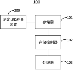
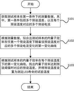
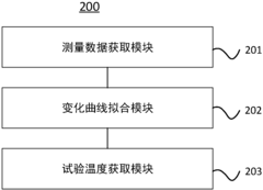
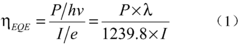
Method and device for measuring service life of LED
PatentActiveCN108152698A
Innovation
- By obtaining the measurement data of the test sample at multiple preset temperatures and currents, the change curve of the internal quantum efficiency is fitted, and the temperature that reaches the preset threshold is found as the test temperature to shorten the test time.
Luminous flux measurement device using standard light source in narrow beam for LED, and testing method
PatentInactiveCN100476389C
Innovation
- Design a testing device using a narrow beam standard light source, including an integrating sphere, a narrow aperture optical fiber and a multi-channel micro spectrometer. Through narrow beam standard light source calibration and spectral calibration, precise testing of LED luminous flux can be achieved, avoiding the need for Screen self-absorption and temperature effects.
Industry Standards and Certification Requirements
The microLED industry is currently navigating a complex landscape of standards and certification requirements that vary significantly across regions and applications. The International Electrotechnical Commission (IEC) has established several standards relevant to microLED luminance testing, including IEC 62341 for OLED displays, which serves as a reference point for emerging microLED standards. Similarly, the International Committee for Display Metrology (ICDM) has published the Information Display Measurements Standard (IDMS), which provides methodologies for measuring display performance characteristics including luminance and color.
In the United States, the Society for Information Display (SID) and the Video Electronics Standards Association (VESA) have been instrumental in developing display performance standards that are gradually incorporating microLED-specific metrics. VESA's DisplayHDR certification program, while primarily focused on LCD and OLED technologies, is evolving to address the unique capabilities of microLED displays, particularly their exceptional brightness ranges and contrast ratios.
The European Union has implemented the Energy-related Products Directive (ErP), which mandates energy efficiency requirements for displays. As microLED technology promises significant energy efficiency improvements, manufacturers must demonstrate compliance with these standards through standardized luminance and power consumption testing methodologies. Additionally, the EU's Restriction of Hazardous Substances (RoHS) directive impacts material selection for microLED manufacturing.
In Asia, particularly in Japan and South Korea, industry consortia have established their own certification programs. Japan's JEITA (Japan Electronics and Information Technology Industries Association) and Korea's KDIA (Korea Display Industry Association) have developed testing protocols specifically addressing the unique characteristics of microLED displays, including luminance uniformity across miniaturized pixel arrays and lifetime degradation patterns.
For lifetime metrics, the industry is working toward standardizing accelerated aging test protocols. Current standards typically require testing under various temperature and humidity conditions, with continuous operation at specified brightness levels. The JEDEC Solid State Technology Association's standards for semiconductor device reliability testing provide some guidance, but microLED-specific lifetime testing standards remain under development, with particular attention to the relationship between driving current, operating temperature, and luminance degradation over time.
Certification requirements for automotive applications of microLED displays are especially stringent, with standards such as AEC-Q102 for optoelectronic components requiring extensive reliability testing, including luminance stability under extreme temperature conditions and accelerated aging tests simulating years of operation in vehicular environments.
Environmental Impact of MicroLED Manufacturing and Testing
The manufacturing and testing processes of MicroLED devices present significant environmental considerations that warrant careful examination. The production of MicroLED displays involves several energy-intensive processes, including epitaxial growth, lithography, etching, and transfer techniques. These processes consume substantial electrical power and often require specialized cleanroom environments with controlled temperature, humidity, and air filtration systems that further increase energy consumption. Additionally, the manufacturing process utilizes various chemicals including solvents, acids, and rare earth materials that pose potential environmental hazards if not properly managed.
Water usage represents another critical environmental factor in MicroLED production. The manufacturing process requires ultra-pure water for cleaning and processing, with estimates suggesting that producing a single MicroLED display may consume thousands of liters of water. This intensive water usage raises concerns about resource depletion, particularly in regions already experiencing water scarcity.
The testing phase of MicroLED devices also contributes to environmental impact through energy consumption. Luminance testing equipment, lifetime testing chambers, and thermal cycling systems operate continuously for extended periods, sometimes weeks or months, to validate device performance and reliability. These testing procedures, while necessary for quality assurance, represent a significant energy footprint in the product development cycle.
Waste management presents additional challenges. Failed devices, test samples, and chemical byproducts from both manufacturing and testing processes require specialized disposal procedures. Particularly concerning are the gallium nitride compounds and rare earth elements used in MicroLED fabrication, which can be environmentally persistent if improperly disposed of.
Carbon footprint assessments of MicroLED manufacturing indicate that the industry faces sustainability challenges, though comparative analyses suggest potential advantages over traditional LCD and OLED technologies in terms of lifecycle environmental impact. MicroLED displays typically consume less power during operation, potentially offsetting some manufacturing impacts over the product lifetime.
Recent industry initiatives have focused on developing more sustainable manufacturing and testing protocols. These include closed-loop water recycling systems, energy-efficient testing procedures that utilize predictive modeling to reduce physical testing requirements, and chemical substitution programs aimed at replacing hazardous substances with more environmentally benign alternatives. Several leading manufacturers have established environmental management systems certified to ISO 14001 standards, demonstrating commitment to continuous improvement in environmental performance.
Unlock deeper insights with Patsnap Eureka Quick Research — get a full tech report to explore trends and direct your research. Try now!
Generate Your Research Report Instantly with AI Agent
Supercharge your innovation with Patsnap Eureka AI Agent Platform!