Inline Inspection Testing and Repair Strategies for MicroLED Yield Improvement
AUG 25, 20259 MIN READ
Generate Your Research Report Instantly with AI Agent
Patsnap Eureka helps you evaluate technical feasibility & market potential.
MicroLED Inspection Background and Objectives
MicroLED technology represents a significant advancement in display technology, offering superior brightness, energy efficiency, and color accuracy compared to traditional LED and OLED displays. The evolution of this technology began in the early 2000s with the development of microscopic LED components, progressing through various research phases to reach today's commercial viability threshold. This technological trajectory has been characterized by continuous miniaturization of LED chips and improvements in mass transfer processes.
The primary objective of inline inspection testing and repair strategies for MicroLED is to address the critical yield challenges that currently impede mass production and widespread market adoption. With millions of microscopic LED elements in a single display, even minimal defect rates can significantly impact overall product quality and manufacturing costs. The industry aims to develop robust inspection methodologies capable of identifying defects at various production stages with high accuracy and efficiency.
Current technical goals include achieving sub-micron precision in defect detection, implementing real-time monitoring systems that can operate at production speeds, and developing repair technologies that can address identified defects without compromising display performance. These objectives align with the broader industry goal of reducing production costs while maintaining exceptional display quality.
The technological evolution trend points toward increasingly automated and AI-enhanced inspection systems that can learn and adapt to new defect patterns. Integration of machine learning algorithms with high-resolution optical inspection tools represents a promising direction for improving detection accuracy while reducing false positives that can unnecessarily slow production.
Another significant trend is the development of non-destructive testing methodologies that can evaluate MicroLED performance characteristics without damaging the delicate structures. These include advanced optical characterization techniques, electrical performance measurements, and thermal analysis methods that collectively provide comprehensive quality assessment.
The ultimate technical objective is to establish a closed-loop manufacturing system where inspection data directly feeds back into process control, enabling continuous optimization of production parameters. This approach aims to shift from reactive defect detection to proactive defect prevention, fundamentally transforming the yield management paradigm for MicroLED manufacturing.
As the technology continues to mature, inspection and repair strategies must evolve to address increasingly complex integration challenges, particularly as MicroLED displays move toward higher resolutions and more diverse form factors including flexible and transparent applications.
Market Analysis for High-Yield MicroLED Displays
The MicroLED display market is experiencing significant growth, driven by increasing demand for high-resolution, energy-efficient display technologies across multiple sectors. Current market projections indicate that the global MicroLED market is expected to reach $19.4 billion by 2026, with a compound annual growth rate of 89.3% from 2021 to 2026. This explosive growth is primarily fueled by applications in smartwatches, smartphones, televisions, augmented reality (AR), and virtual reality (VR) devices.
Consumer electronics represents the largest market segment, with major manufacturers like Samsung, Apple, and LG investing heavily in MicroLED technology development. The automotive sector is emerging as another significant market, with premium vehicle manufacturers incorporating MicroLED displays in dashboard systems and entertainment consoles due to their superior brightness and durability in varying light conditions.
Market research indicates that yield improvement remains the most critical factor affecting mass production and market penetration of MicroLED displays. Current yield rates for high-resolution MicroLED panels typically range between 60-70%, significantly lower than the 90%+ rates achieved in mature LCD and OLED production. This yield gap translates directly to higher production costs, with MicroLED displays currently priced 4-5 times higher than comparable OLED alternatives.
Industry surveys reveal that manufacturers willing to invest in advanced inline inspection and repair technologies can achieve up to 15-20% improvement in overall yield rates. This improvement directly correlates with a 30-40% reduction in production costs, potentially accelerating market adoption by 2-3 years compared to standard production approaches.
Regional analysis shows Asia-Pacific dominating the MicroLED manufacturing landscape, with South Korea, Taiwan, and China accounting for approximately 78% of global production capacity. North America leads in technology development and intellectual property, while Europe focuses on specialized applications in automotive and medical displays.
Consumer demand analysis indicates strong interest in MicroLED benefits, with 67% of surveyed premium device users citing improved brightness, energy efficiency, and longevity as features worth paying a premium for. However, price sensitivity remains high, with market penetration expected to remain limited to premium segments until production yields improve sufficiently to bring costs down by at least 50-60% from current levels.
The market forecast suggests that manufacturers who successfully implement comprehensive inline inspection and repair strategies will gain significant competitive advantages, potentially capturing up to 40% market share in their respective segments within the first three years of mass production capability.
Current Challenges in MicroLED Inline Testing
MicroLED technology faces significant challenges in inline testing processes that directly impact production yields. The complexity of these displays, with millions of microscopic LEDs, creates unprecedented testing requirements that conventional methods struggle to address. Current inspection systems lack sufficient resolution and speed to detect all defects in high-volume manufacturing environments, particularly for sub-10μm LED chips.
One major challenge is the development of high-speed, high-precision optical inspection systems capable of identifying defects at the microscopic level without damaging delicate components. Existing systems often require trade-offs between inspection speed and accuracy, creating bottlenecks in production lines. The industry currently lacks standardized testing protocols specifically designed for MicroLED manufacturing, forcing manufacturers to adapt semiconductor or traditional LED testing approaches with limited success.
Electrical testing presents another significant hurdle, as conventional probe-based methods risk damaging the miniature LED structures. Contact-based testing can introduce new defects during the inspection process itself, creating a counterproductive scenario. Non-contact testing alternatives remain in early development stages and have not yet achieved the necessary reliability for mass production environments.
The detection of "dark pixels" - LEDs that pass electrical tests but fail to emit light at specified brightness levels - represents a particularly challenging defect type. These failures may result from various causes including crystal defects, poor electrical connections, or degraded phosphor layers, requiring multiple testing methodologies to identify comprehensively.
Data management systems for inline testing face overwhelming challenges due to the massive volume of information generated during inspection. A single 4K MicroLED display may contain over 24 million individual LEDs, each requiring multiple test parameters. Processing this data in real-time to make repair or rejection decisions demands computing infrastructure beyond what most manufacturers currently deploy.
Temperature and environmental control during testing introduces additional complexity, as MicroLED performance characteristics vary significantly with temperature fluctuations. Maintaining consistent testing conditions across large panels requires sophisticated environmental chambers that add cost and complexity to production lines.
Finally, correlation between inline test results and final product performance remains problematic. Current testing methodologies struggle to accurately predict how detected defects will manifest in finished displays, leading to either excessive rejection rates or quality issues in final products. The industry urgently needs improved predictive models that can translate inline test data into reliable yield forecasts and quality metrics.
Existing Inline Repair Solutions for MicroLED
01 Automated inspection and testing systems for MicroLED
Automated systems are employed for inline inspection and testing of MicroLED displays. These systems utilize advanced imaging technologies and algorithms to detect defects in MicroLED arrays during production. The automation helps maintain consistency in quality control while significantly improving throughput compared to manual inspection methods. These systems can identify various defect types including dead pixels, brightness variations, and alignment issues in real-time during the manufacturing process.- Automated inspection and testing systems for MicroLED: Automated systems are employed for inline inspection and testing of MicroLED displays. These systems utilize advanced imaging technologies and algorithms to detect defects in MicroLED arrays. The automation helps in maintaining consistency in quality control while increasing throughput in the manufacturing process. These systems can identify various defects including dead pixels, brightness variations, and alignment issues in real-time during production.
- Repair strategies for defective MicroLED pixels: Various repair strategies have been developed to address defective MicroLED pixels identified during inspection. These include laser repair techniques, redundancy-based approaches where backup LEDs can be activated, and pixel remapping methods. The repair processes can be performed inline without disrupting the manufacturing flow, which helps maintain high production yields. Advanced repair algorithms determine the most efficient repair strategy based on the type and location of defects.
- Yield enhancement through predictive analytics: Predictive analytics and machine learning algorithms are implemented to enhance MicroLED manufacturing yields. These systems analyze historical inspection data to identify patterns and predict potential failure points before they occur. By implementing preventive measures based on these predictions, manufacturers can significantly improve yield rates. The analytics systems continuously learn from production data to refine their predictive capabilities and optimization recommendations.
- In-situ monitoring and real-time adjustment techniques: In-situ monitoring systems provide real-time feedback during MicroLED manufacturing, allowing for immediate process adjustments. These systems incorporate sensors that monitor critical parameters such as temperature, pressure, and alignment during production. When deviations are detected, automated systems make real-time adjustments to process parameters to maintain optimal conditions. This approach minimizes defect formation and improves overall yield by addressing issues before they affect product quality.
- Fault isolation and defect classification methods: Advanced fault isolation and defect classification methods are employed to categorize MicroLED defects based on their characteristics and root causes. These methods utilize image processing, spectral analysis, and electrical testing to precisely identify defect types. By accurately classifying defects, appropriate repair strategies can be selected, and manufacturing processes can be refined to prevent similar defects in future production. This systematic approach to defect management contributes significantly to yield improvement.
02 Repair strategies for defective MicroLED pixels
Various repair strategies have been developed to address defective MicroLED pixels identified during inspection. These include laser repair techniques, redundancy-based approaches where backup LEDs can be activated, and pixel remapping methods. The repair processes can be performed inline without removing panels from the production line, which helps maintain manufacturing efficiency. Effective repair strategies are crucial for improving overall yield rates in MicroLED production.Expand Specific Solutions03 Yield enhancement through predictive analytics and machine learning
Advanced data analytics and machine learning algorithms are implemented to predict potential failures and optimize the MicroLED manufacturing process. By analyzing historical inspection data, these systems can identify patterns that lead to defects and recommend process adjustments before failures occur. This predictive approach helps manufacturers continuously improve yield rates by addressing root causes rather than just detecting and repairing defects after they occur.Expand Specific Solutions04 Integration of testing throughout the MicroLED manufacturing process
Testing procedures are integrated at multiple stages of the MicroLED manufacturing process rather than only at final inspection. This multi-stage approach includes wafer-level testing, transfer process verification, and post-bonding inspection. By identifying defects earlier in the production cycle, manufacturers can reduce waste and improve overall yield. The integrated testing approach also provides valuable feedback for process optimization.Expand Specific Solutions05 Novel equipment and methodologies for high-precision MicroLED inspection
Specialized equipment and methodologies have been developed specifically for the high-precision requirements of MicroLED inspection. These include high-resolution optical systems, electrical testing apparatus, and thermal imaging technologies that can detect subtle defects invisible to conventional inspection methods. The equipment is designed to handle the extremely small dimensions of MicroLEDs while maintaining high throughput. These innovations address the unique challenges of MicroLED manufacturing where defects at microscopic scales can significantly impact display performance.Expand Specific Solutions
Key Industry Players in MicroLED Testing Equipment
The MicroLED inline inspection testing and repair market is currently in its early growth phase, characterized by rapid technological development and increasing adoption across display manufacturing. The market is projected to expand significantly as MicroLED technology matures, driven by applications in AR/VR, automotive displays, and consumer electronics. Companies like VueReal, Applied Materials, and Samsung Electronics are leading innovation with advanced inspection solutions, while KLA Corp. and PDF Solutions offer specialized yield management systems. BOE Technology and Japan Display are developing integrated testing approaches for mass production. The competitive landscape features both established semiconductor equipment manufacturers and emerging startups focusing on novel inspection techniques, automated repair strategies, and AI-driven defect detection to address the critical yield challenges in MicroLED manufacturing.
VueReal, Inc.
Technical Solution: VueReal has developed an advanced Continuous Pixelation technology for MicroLED manufacturing that integrates inline inspection and repair strategies. Their system employs high-precision transfer printing combined with real-time defect detection using machine vision algorithms that can identify defects as small as 1-2 microns[1]. The inspection system works in tandem with their proprietary Solid Printing technology, which allows for selective repair of defective pixels without disturbing adjacent functional elements. VueReal's approach incorporates closed-loop feedback between inspection and repair stations, enabling adaptive process control that continuously optimizes transfer yield based on historical defect data[3]. Their technology achieves transfer yields exceeding 99.99% for sub-10μm microLEDs, with repair capabilities that can address both electrical and optical defects through redundant circuit pathways and laser-based correction methods.
Strengths: Achieves industry-leading transfer yields exceeding 99.99% for sub-10μm microLEDs; integrated inspection-repair feedback loop enables continuous process improvement; proprietary Solid Printing technology allows for targeted repairs without affecting adjacent pixels. Weaknesses: System requires significant capital investment; repair strategies may increase overall production time; technology is still scaling to accommodate larger display formats.
Applied Materials, Inc.
Technical Solution: Applied Materials has developed a comprehensive inline inspection and repair ecosystem for MicroLED manufacturing called the "Integrated MicroLED Yield Management System." This system combines optical and electrical testing methodologies at multiple production stages. Their approach utilizes high-resolution automated optical inspection (AOI) with sub-micron detection capabilities, complemented by electrical parametric testing that can identify both catastrophic and parametric failures[2]. The inspection data feeds into their proprietary AI-driven defect classification system that categorizes defects based on type, severity, and reparability. For repair strategies, Applied Materials employs a multi-modal approach including laser repair stations for pixel reconnection, redundant circuit activation, and selective material deposition for addressing various defect types[4]. Their system features real-time statistical process control (SPC) that monitors yield trends across production batches, enabling predictive maintenance and process adjustments before yield issues become critical. The technology has demonstrated the ability to improve overall MicroLED yields by 30-40% in production environments through the combination of early defect detection and efficient repair methodologies[5].
Strengths: Comprehensive end-to-end solution covering multiple inspection points in the manufacturing process; advanced AI-driven defect classification enables targeted repair strategies; proven yield improvements of 30-40% in production environments. Weaknesses: High implementation complexity requiring significant process integration; repair strategies may not be equally effective for all defect types; system requires regular calibration and maintenance to maintain optimal performance.
Critical Patents in MicroLED Defect Detection
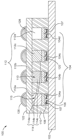
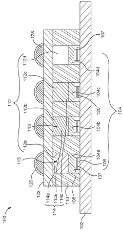
Repair techniques for micro-led devices and arrays
PatentPendingUS20220199605A1
Innovation
- The implementation of defect mapping techniques, color conversion, and spatial variation methods to redistribute the luminance contribution of defective sub-pixels to spare sub-pixels, allowing for effective repair without the need for additional micro devices, by using predefined, surround, or weighted mapping strategies to share brightness between spare sub-pixels and calibrating the system to minimize visual artifacts.
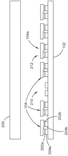
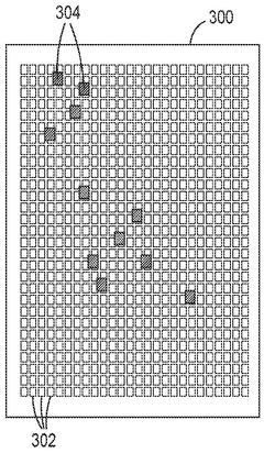
Die repair process in microled display fabrication
PatentWO2025034875A1
Innovation
- The proposed solution involves a method and system for repairing defective micro-LEDs during fabrication, which includes determining maps of defective areas, trimming defective micro-LEDs, applying repair materials, and bonding repair micro-LEDs using advanced image analysis and laser processing techniques.
Cost-Benefit Analysis of Repair vs. Redundancy
In the MicroLED manufacturing landscape, a critical strategic decision revolves around whether to invest in repair capabilities or implement redundancy designs. This cost-benefit analysis examines both approaches to determine optimal yield improvement strategies.
Repair technologies for MicroLED defects require significant capital investment in specialized equipment, including laser repair systems, probe stations, and advanced imaging tools. Initial setup costs typically range from $2-5 million for basic repair capabilities, with ongoing operational expenses of $500,000-800,000 annually for maintenance, calibration, and skilled technician staffing. However, these investments can be justified when repair success rates exceed 70%, particularly for high-value, large-format MicroLED displays where each panel represents substantial material and processing costs.
Redundancy strategies, conversely, involve designing additional LED elements into the display architecture that can be activated when primary pixels fail. This approach increases initial silicon and manufacturing costs by approximately 15-25%, depending on redundancy levels implemented. The primary advantage lies in simplified testing procedures and elimination of complex repair steps, potentially reducing overall production cycle time by 30-40%.
Market analysis indicates that repair strategies prove most economical for premium, low-volume products where unit prices can absorb repair costs. Several leading manufacturers have reported ROI achievement within 18-24 months for repair equipment investments. Redundancy approaches demonstrate superior economics for high-volume, consumer-grade applications where production throughput and simplified processes outweigh the additional material costs.
The decision matrix becomes more complex when considering yield rates across different manufacturing stages. For mass transfer yields below 99.5%, redundancy alone often proves insufficient, necessitating complementary repair capabilities. Conversely, when transfer yields exceed 99.7%, redundancy designs frequently provide adequate coverage without repair intervention.
Recent industry case studies reveal hybrid approaches gaining traction, where limited redundancy is combined with targeted repair capabilities focused on specific defect types. This balanced strategy has demonstrated optimal cost-effectiveness for mid-range MicroLED products, reducing total quality costs by 22-35% compared to exclusive reliance on either approach.
The long-term economic analysis must also consider technology maturation curves. As repair technologies advance, their costs typically decrease 15-20% annually, while effectiveness improves. This suggests that repair-centric strategies may become increasingly viable across broader product segments as the MicroLED industry matures.
Mass Production Scalability Considerations
Scaling MicroLED technology for mass production presents significant challenges that must be addressed to achieve commercial viability. Current manufacturing processes for MicroLED displays demonstrate limited throughput capabilities, with production rates significantly lower than those established for LCD and OLED technologies. This throughput limitation directly impacts cost structures and market competitiveness, necessitating substantial improvements in production efficiency.
The implementation of inline inspection, testing, and repair strategies must be evaluated within the context of high-volume manufacturing environments. Conventional testing methods often create production bottlenecks, particularly when applied to the millions of individual pixels in a MicroLED display. Automated optical inspection (AOI) systems require optimization for speed without compromising detection accuracy, as false positives can unnecessarily slow production while missed defects impact final yield.
Equipment scalability represents another critical consideration. Current repair tools typically operate in serial processing modes, addressing defects individually. For mass production scenarios, parallel processing capabilities must be developed to handle multiple repair operations simultaneously. This transition from serial to parallel processing demands significant engineering innovation in both hardware design and control software.
Integration of inspection and repair processes into continuous production lines presents additional complexity. The physical footprint of testing and repair equipment must be minimized while maintaining functionality, as factory floor space directly impacts production economics. Moreover, the capital expenditure required for comprehensive inline testing systems must be balanced against the yield improvements they deliver to ensure positive return on investment.
Data management infrastructure represents an often-overlooked aspect of scalability. The volume of test data generated during mass production of MicroLED displays is substantial, requiring robust systems for collection, analysis, and storage. Real-time processing of this data is essential for immediate defect identification and repair decision-making, necessitating high-performance computing resources integrated with production equipment.
Labor requirements and skill development pathways must also be considered. While automation reduces direct labor needs, specialized technicians are required for system maintenance and optimization. Training programs and knowledge transfer mechanisms must be established to support global deployment of MicroLED production facilities, particularly as manufacturing expands beyond initial pilot sites.
Ultimately, successful scaling of MicroLED production depends on establishing a balanced ecosystem of inspection, testing, and repair technologies that can evolve in parallel with core manufacturing processes. Strategic investment in these supporting technologies is essential for achieving the yield improvements necessary for commercial viability in consumer electronics markets.
Unlock deeper insights with Patsnap Eureka Quick Research — get a full tech report to explore trends and direct your research. Try now!
Generate Your Research Report Instantly with AI Agent
Supercharge your innovation with Patsnap Eureka AI Agent Platform!